Determination of trap density-of-states distribution of nitrogendoped ultrananocrystalline diamond/hydrogenated amorphous carbon composite films
Mahmoud Shaban
1Department of Electrical Engineering, College of Engineering, Qassim University, Unaizah 56452, Saudi Arabia
2Department of Electrical Engineering, Faculty of Engineering, Aswan University, Aswan 81542, Egypt
Abstract: Thin films comprising nitrogen-doped ultrananocrystalline diamond/hydrogenated amorphous-carbon (UNCD/a-C:H)composite films were experimentally investigated.The prepared films were grown on Si substrates by the coaxial arc plasma deposition method.They were characterized by temperature-dependent capacitance-frequency measurements in the temperature and frequency ranges of 300–400 K and 50 kHz–2 MHz, respectively.The energy distribution of trap density of states in the films was extracted using a simple technique utilizing the measured capacitance-frequency characteristics.In the measured temperature range, the energy-distributed traps exhibited Gaussian-distributed states with peak values lie in the range:2.84 ×10¹⁶–2.73 × 10¹⁷ eV–1 cm–3 and centered at energies of 120–233 meV below the conduction band.These states are generated due to a large amount of sp2-C and π-bond states, localized in GBs of the UNCD/a-C:H film.The attained defect parameters are accommodating to understand basic electrical properties of UNCD/a-C:H composite and can be adopted to suppress defects in the UNCD-based materials.
Key words: nitrogen-doping; nanodiamond; UNCD/a-C:H; capacitance-frequency characterization; trap density-of-states
1.Introduction
Diamond was extensively characterized as a wide bandgap (5.47 eV) semiconducting material that possessing distinguished thermal, physical, electrical, optical, and electronic properties[1–4].In recent years, diamond-based electronic devices, including rectifier and Schottky diodes, light-emitting diodes, photodetectors, CO2gas detectors, and MOSFETs, are experimentally produced and repeatedly characterized[4–6].Based on grain sizes, the synthetic diamond can be grown in many forms:single-crystalline, microcrystalline, nanocrystalline, and ultrananocrystalline diamond (UNCD).In recent years, UNCD films were synthesized using various deposition methods such as plasma chemical vapor deposition(CVD), hot-filament CVD, microwave-plasma CVD, pulsedlaser deposition (PLD), and coaxial-arc plasma deposition(CAPD)[7–32].One unique form of UNCD is what is namely recognized as the UNCD/hydrogenated amorphous-carbon (UNCD/a-C:H).This phase comprises a high density of UNCD fine grains embedded in an a-C matrix, produced in hydrogen ambient during film preparation.Boron and nitrogen were examined as an efficient dopant of UNCD to produce p-type and n-type conduction, respectively[10,11].Microstructure analysis, including XRD, TEM, and Raman spectroscopy, confirmed that UNCD films comprising a grain size of 3–5 nm in addition to grain-boundaries (GBs) with widths of 1–1.5 nm[16–20].The film structure is composed of sp2and sp3hybridized carbon mixture[12–14].The UNCD GBs commonly contain a large amount of sp2-C bonds, while the grains contain sp3-C bonds[11,14].The room-temperature electrical conductivity of the low-nitrogen content (3 at.%) UNCD/a-C:H films produced by CAPD was measured to be 3.5 × 10⁻⁴Ω–1cm–1.The latter value was increased to be 0.2 Ω–1cm–1, as the nitrogen content in the films increased to 12.9 at.%[24].The carrier density of the 3 at.% nitrogen-doped films was deduced to be 7.5 × 1016cm–3[25].The nitrogen incorporation into the UNCD/a-C:H films was confirmed by a high-resolution XPS measurement[30].Experimental investigations have shown that increasing nitrogen incorporation in the grown films increases the amount of sp2at the expense of sp3bonds.This is might be the main reason for the increased electrical conductivity of the N2-doped of UNCD films.Additionally, the nitrogen amount in the grown films strongly affects the structure and GBs volume in the films[11,14].A hopping conduction mechanism has been theoretically proposed for carrier transport at GBs in UNCD/a-C:H due to π-states of the sp2-bonded carbon[13].This has been experimentally confirmed later as reported in Ref.[14].Nitrogen atoms incorporate into the GBs rather than the UNCD grains, which results in the creation of localized electronic states within the N2-doped UNCD/a-C:H bandgap (1.28 eV).Electron spin resonance (ESR) measurement of UNCD/a-C films exhibited a dangling bond density of 1022cm–3[21].These dangling bonds might formulate localized electronic states in the UNCD bandgap.More recently, surface states in Pd/n-type UNCD/a-C:H deposited on Si substrates was studied[22].The surface states density in Pd/n-type UNCD/a-C:H films was evaluated to be 1.7 × 1015cm–2eV–1for the slow response states, which decreased to 2.0 ×1014cm–2eV–1for the high-frequency response states[22].Although the electrical and optical properties of N2-doped UNCD/a-C:H films grown by the CAPD method have been extensively studied[23–32], there have been very limited reports on defects in these films.In this study, defect properties and energy-distributed trap density-of-states (DOS) in UNCD/a-C:H films have been experimentally investigated.
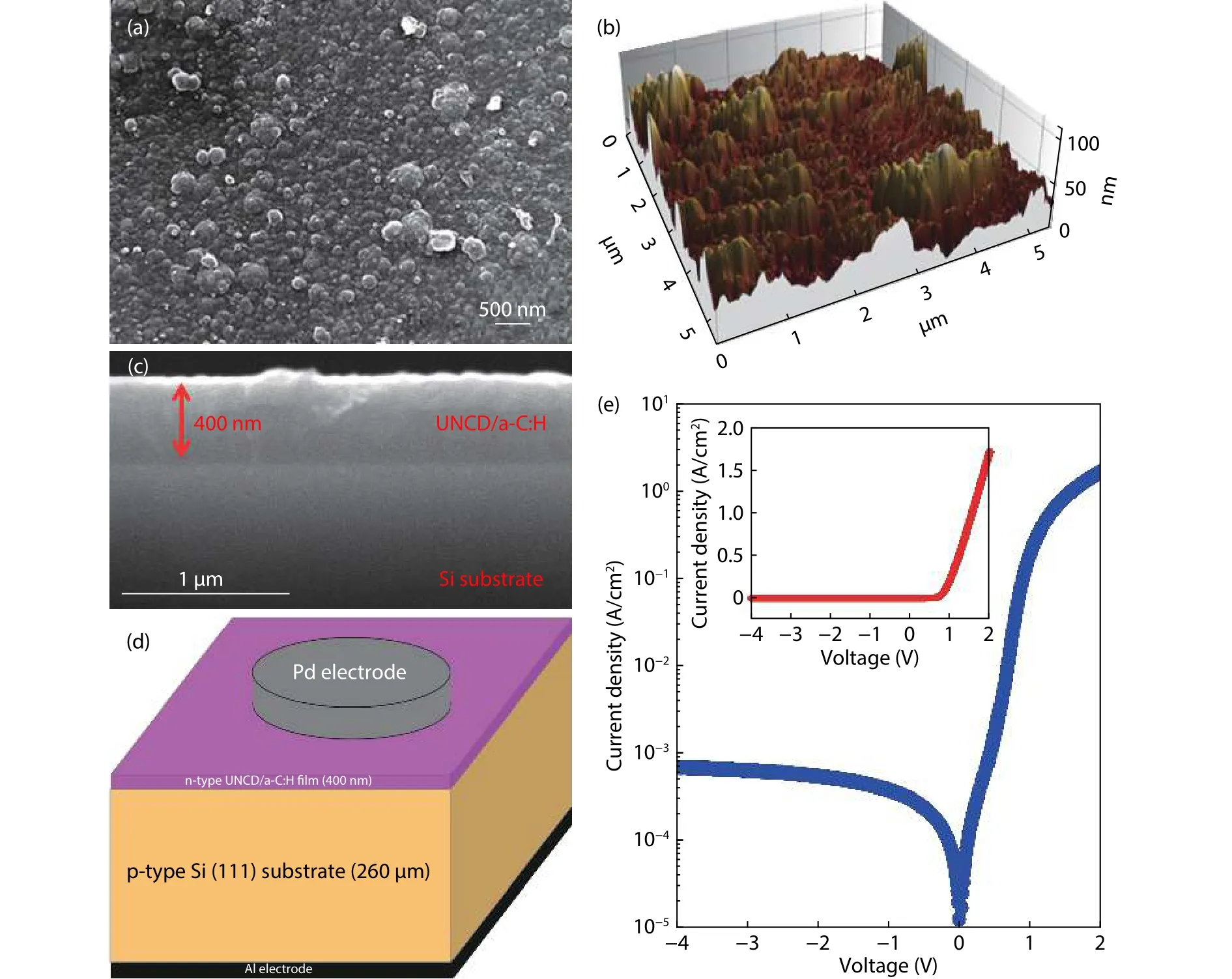
Fig.1.(Color online) (a) Top-view FESEM images, (b) AFM image of UNCD/a-C:H film surface, (c) cross-sectional FESEM image, (d) schematic representation, and (e) semi-logarithmic and linear (inset) J–V characteristics of N2-doped (UNCD/a-C:H)/p-Si heterojunctions.
2.Experimental details
Thin films (thicknesses:400 nm) of N2-doped UNCD/a-C:H composite were deposited on p-type Si(111) substrates(resistivities:1–1.3 Ω·cm).A coaxial arc plasma gun (CAPG)equipped with pure graphite targets was fixed inside the deposition chamber.A capacitor of 720μF and 100 V power supply was used to operate the CAPG[21–32].The chamber was initially evacuated to a pressure less than 10–5Pa, using a turbo molecular pump.The Si substrates were gradually heated to 550 °C then the plasma was ignited in H2/N2mixed-gases ambient.The plasma discharge rate was set to be 5 pulse/s.During the film deposition, the ambient pressure was maintained constant at a pressure of 53 Pa.Immediately after the film deposition, the samples were transferred to a magnetron sputtering chamber to form device electrodes.A circularshaped Pd electrode was deposited on the top surface of the UNCD/a-C:H film, while an Al electrode was deposited on the bottom surface of the Si substrate.The film surface morphology was examined by field-emission scanning electron microscope (FESEM) and atomic force microscopy (AFM).The prepared devices were characterized by the current-density–voltage (J–V) and temperature-dependent capacitance–frequency–voltage (C–f–V) method.TheC–f–Vmeasurements were carried out in temperature, frequency, and DC bias voltage ranges of 300–400 K, 50 kHz –2 MHz, –5–+5 V, respectively.
3.Results and discussion
Fig.1(a) illustrates the FESEM top-view image of UNCD/a-C:H film, deposited by the CAPD method.The formed N2-doped UNCD/a-C:H films comprise an enormous number of dissimilar nano-sized UNCD crystals surrounded by the a-C:H matrix.UNCD/a-C:H films, produced by CAPD and their surface morphology examined by AFM, typically demonstrate smooth surfaces.As shown in Fig.1(b), the film surface roughness is within 100 nm with root-mean-square (rms) of 9–12 nm.These values are somewhat larger than those observed for undoped UNCD/a-C:H films (rms:8 nm).As illustrated in Fig.1(c), the cross-sectional FESEM image clearly illustrates a sharp film/substrate interface.This property is essential to accomplish heterojunction devices with good electric performance.Fig.1(d) depicts a schematic representation of the fabricated (UNCD/a-C:H)/Si device with a film thickness of400 nm and p-type Si(111) substrate thickness of 260μm.Circular-shaped Pd ohmic contacts were formed on the film top surface, while Al ohmic contact was formed on the backside of the substrate.The diameter of the Pd electrode is 0.7 mm and the device effective device area is 3.8 × 10⁻³cm2.Fig.1(e) and (inset) show typicalJ–Vcharacteristics of N2-doped UNCD/a-C:H film deposited on the Si substrate.The characteristics display noticeable rectifying action with a rectification ratio of more than three orders of magnitude at forward and reverse voltages of ± 2 V.This result confirms that the N2-doped UNCD/a-C:H films possess n-type conduction and a formulae pn heterojunction diode with the p-type Si substrate.The turn-on voltage of the junction, extracted from the linear plot of the forward biasJ–Vcharacteristics, was approximately 0.75 V.In the reverse bias direction, the leakage current density was 0.7 mA/cm2at a reverse bias of –4 V.This current leakage might be attributed to thermally activated generation-recombination processes of charge carriers.Due to the presence of a considerable number of defects and charge-trapping centers in the UNCD/a-C:H film in addition to the existence of trap states at the film/substrate interface,the generation-recombination processes predominantly occur in the bulk and surface of the film.
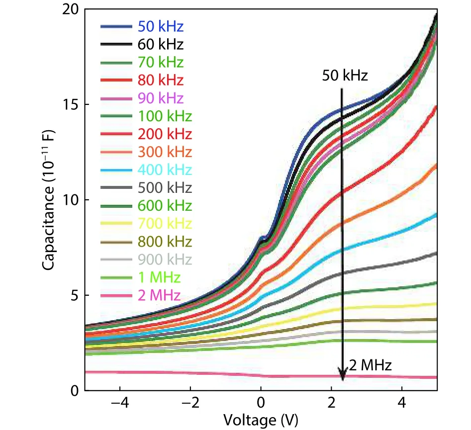
Fig.2.(Color online) C–V characteristics of (N2-doped UNCD/a-C:H)/ptype Si heterojunction, measured at different frequencies from 50 kHz to 2 MHz.
Fig.2 demonstrates frequency-dependentC–Vcharacteristics of the N2-doped (UNCD/a-C:H)/p-Si device.The measured capacitance exhibited a strong dependence on both the applied DC bias voltage and the AC signal frequency.This dependence reveals the existence of a considerable number of defects and localized electronic states in both the UNCD/a-C:H film and the (n-UNCD/a-C:H)/p-Si interface.The capacitance increases with increasing the forward bias voltage,while it strongly decreases with increasing the reverse bias voltage.This can be referred to as diffusion and depletion capacitances commonly observed in conventional pn junctions.Under forward bias, the diffusion capacitance dominates and rises with increasing the applied voltage, as it is proportional to the forward current.On the other hand, the depletion capacitance dominates at reverse bias and decays with increasing the reverse bias voltage due to expanding the depletion-layer width.The capacitance also decreases with increasing of the signal frequency.At lower frequencies, the defect states can easily track the AC signal causing excessive capacitance values.At higher frequencies (greater than 100 kHz), the defect states cannot effectively follow the signal frequencies.This action degrades the contribution of the trap states to the total device capacitance measured for each bias voltage.The depletion-layer capacitance (C) is interrelated to the DC bias voltage (V) using the Schottky–Mott equation[33]:
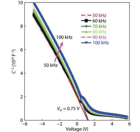
Fig.3.(Color online) C–V characteristics of (N2-doped UNCD/a-C:H)/ptype Si heterojunction, measured at different frequencies from 50 to 100 kHz.

whereqis the electric charge,Ais the device area,ε1andε2are the local permittivities, andN1andN2are doping concentrations of UNCD/a-C:H and Si, respectively.The doping concentration of the UNCD/a-C:H film was extracted using the slope of the1/C2–Vplot and the known parameters of the UNCD/a-C:H film (ε1= 5.68εo, whereεodenotes the free-space permittivity) and those of the p-Si substrate (ε2= 11.9εo, andN2= 1 ×1016cm–3, corresponding to the resistivity of 1–1.3 Ω·cm).Besides, the total depletion-layer width (W) was extracted using the equations[33]:
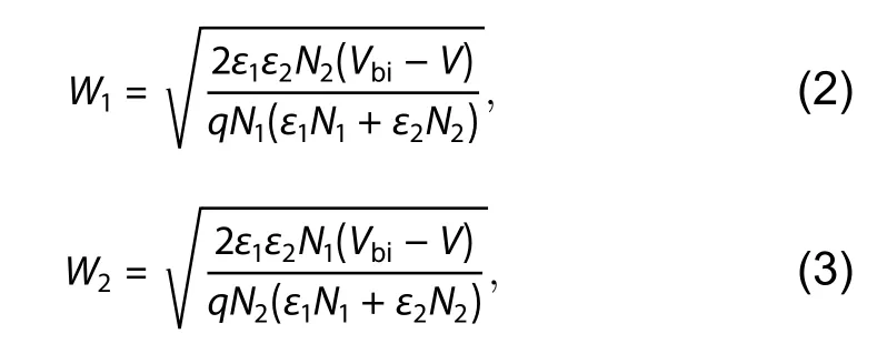
whereW1andW2denote the depletion-region extensions inside the UNCD/a-C:H film and that of the Si substrate, respectively.The heterojunction built-in potential (Vbi) was directly extracted from1/C2–Vplots to be 0.75 V, as shown in Fig.3.The latter values are consistent with that of the turn-on voltage (0.75 V) deduced from the linear plot of the heterojunctionJ–Vcharacteristics, shown in Fig.1(e).The1/C2–Vplots exhibited linear dependence of the applied voltage, demonstrating a homogeneous distribution of donor atoms in the deple-tion layer.The total width of the depletion-layer (W=W1+W2) was extracted to be 322 nm and the doping concentration of the UNCD/a-C:H film was determined to be 1.95 ×1016cm–3.
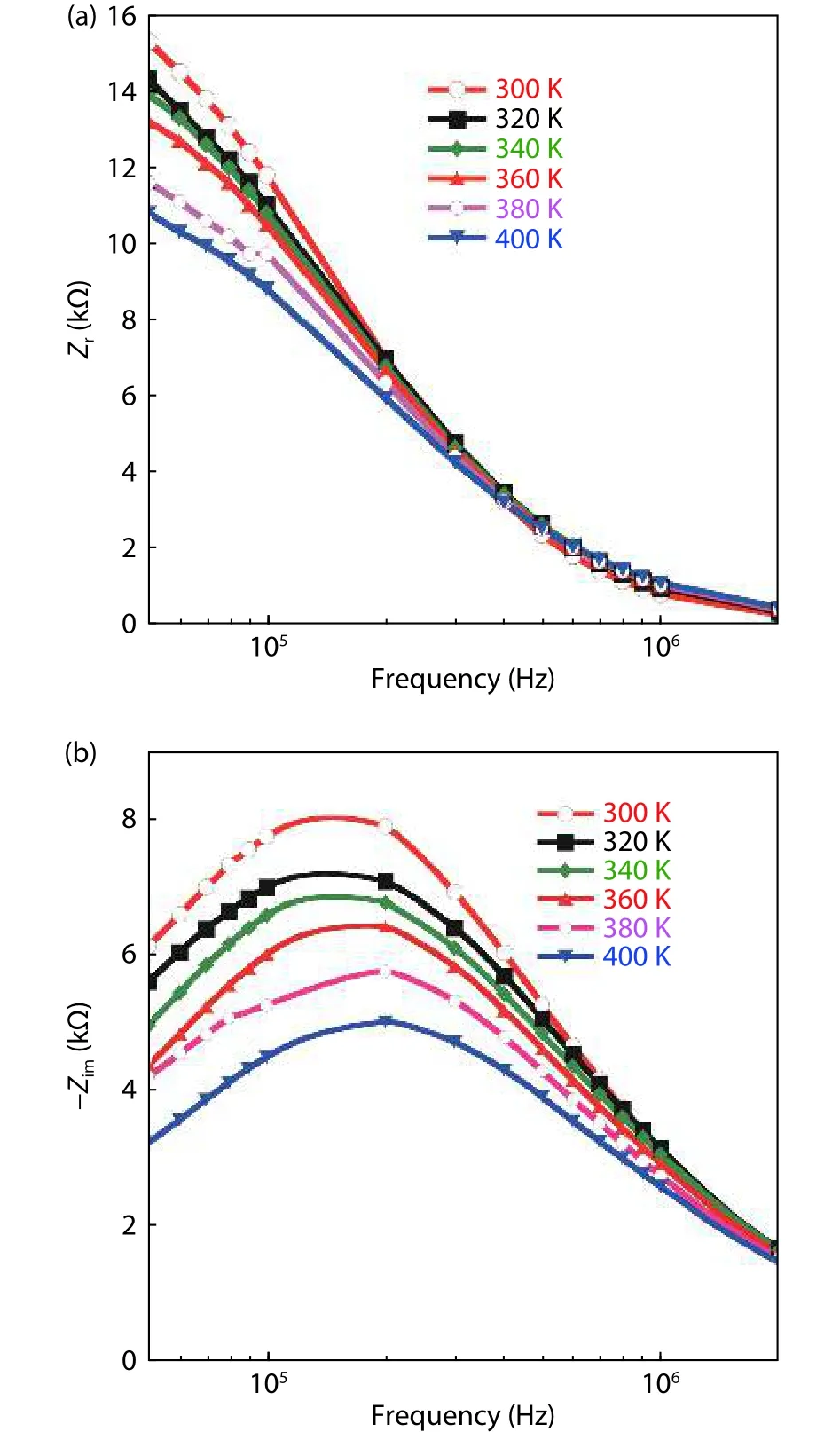
Fig.4.(Color online) Zr and Zim spectra of (N2-doped UNCD/a-C:H)/ptype Si heterojunction, measured at different temperatures from 300 to 400 K.
The complex impedance (Z*) spectroscopy of the heterojunctions was measured in the temperature range of 300–400 K.Z*is commonly expressed as the vector summation of two parts:real (Zr) and imaginary (Zim) impedances.Figs.4(a) and 4(b) show the temperature-dependent spectra ofZrandZim.In this regard,Zrexhibited strong decay with increasing frequency and temperature.This impedance is attributed to carrier transportation resistance in UNCD/a-C:H film in addition to carrier recombination at film/electrode and film/substrate interfaces.Moreover, this resistance arises due to space-charge, dipoles, and electrons polarization in the film and Si substrate.At high frequencies, the polarized charges unable to follow fast changes of the AC signal, thus their influences on the impedance decline gradually with increasing frequency.Furthermore,Zrdecreased with rising of the temperature due to carrier thermal generation from defects in UNCD/a-C:H film.On the other hand,Zimshowed broadening peaks centered at frequencies above 105Hz.The observedZimpeaks were slightly shifted to higher frequencies at increased temperatures.The signal angular-frequency(ω=2πf) at whichZimis maximized can be related to relaxation time constant (τ) using the relation:ωmτ= 1.The time constant for thermal-emission of electrons from a trap state can be computed by[34]:
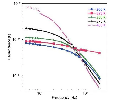
Fig.5.(Color online) C–f characteristics of (N2-doped UNCD/a-C:H)/ptype Si heterojunction, measured at different temperatures.
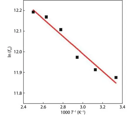
Fig.6.Arrhenius plot of ln(fm) of (N2-doped UNCD/a-C:H)/p-type Si heterojunction.

whereσnis the capture cross-section,vthis the thermal velocity,NCis the DOS in the conduction band,Eais the activation energy of the trap states with respect to the conduction band edge,Kis the Boltzmann constant, andTthe temperature.The termσnνthNCdefines what is called the attempt-to-escape-frequency (υ0)[35].At lower frequencies, charge carriers initiated from the trap centers can effectively trace AC signal,while at a higher frequency they unable to track the fast modulation of the signal.Therefore, the critical energy depth of the traps that are able to contribute to the measured capacitance is essentially determined by the applied signal frequency.This explains well the observed deterioration of device capacitance at frequencies above 105Hz, as illustrated in theC–fcharacteristics shown in Fig.5.Many dia-mond-based devices reveal capacitance values that significantly decrease at frequencies larger than 105Hz[36,37].This demonstrates the existence of noteworthy thermally activated processes including charge relaxation in space-charge regions and carrier emission/capture processes initiated by trap centers which are more likely to have existed at GBs in the UNCD/a-C:H film.

Fig.7.Energy-distributed trap-DOS of N2-doped UNCD/a-C:H film measured (dots) and fitted (lines) data at temperatures of (a) 300 K, (b) 325 K,(c) 350 K, (d) 375 K, and (e) 400 K.

Table 1. Extracted Gaussian-distributed defect parameters of N2-doped UNCD/a-C:H films characterized at different temperatures.
Fig.6 depicts the Arrhenius plot of the extracted values offmfor each measured temperature.At high temperatures,more carriers are emitted from the traps excited by dissipated thermal energy in the UNCD/a-C:H film.Furthermore, as the temperature increases,fmincreases, subsequently the trap response time becomes shorter.The characteristics frequency,υ0, was extracted to be 5.7 × 10⁵Hz using linear fitting to the Arrhenius equation:

The activation energy attained from the slope of the linear fit in the plot was determined to be 46 meV.This value is comparable with those obtained for the N2-doped UNCD films prepared with dissimilar deposition methods[38,39].In this context, the activation energy is greatly affected by the incorporated amount of nitrogen in the UNCD films.The GBs in these films, comprising a considerable amount of sp2-C bonds that are associated with π-bonded states, might be the main reason for the n-type conduction in N2-doped UNCD films[40].Therefore, the activation energy was reduced by increasing of nitrogen doping level in the film.
The trap states frequency response is regularly described in terms of a demarcation energyEf, where this frequency-dependent energy is defined by[41]:

Hence, the trap density-of-states (Nt) is computed by[41]:

The energy distribution of a defect/trap state at an energyEfcan be evaluated by calculating the first derivative of the measured heterojunction capacitance with respect to the signal frequency.
Figs.7(a)–7(e) show defect energy-distributed DOS deduced from Eqs.(6) and (7) using measuredC–fcharacteristics of n-type UNCD/a-C:H films/p-type Si substrate, examined at different temperatures.Despite the noise that appeared in the derived DOS data, resulting from slight inaccuracy of the measuring instrument, particularly at high frequencies, in addition to the dispersion of the capacitance–frequency derivative (dC/df), fitting of the data showed nice consistency with the Gaussian equation:

whereNGis the DOS peak located at an energyEequals to that of a trap energyEtandσdenotes characteristic energy of the trap center.At room temperature, the Gaussian peak of 2.8 × 1016cm–3eV–1located at trap energy of 0.120 eV,with a characteristic energy of 0.064 eV, was deduced.These results are in good agreement with those obtained usingJ–Vcharacterization[32].As the temperature increased, from 300 to 400 K, the extracted peaks were gradually increased and shifted to deeper energy levels as listed in Table 1.
Since nitrogen atoms preferentially integrate into GBs rather than into the UNCD grains, they tend to create additional conduction pathways in the films, causing the increase of electric conductivity of the films due to a significant increase in sp2-C and π-bonds in the composite.Therefore, the defect states are localized mainly in GBs in the UNCD/a-C:H films.The bulk defects, in addition to the interface defects, might be the main causes of the leakage current observed in (ntype UNCD/a-C:H)/p-type Si heterojunction devices.Suppression of these defects can be attainable through the optimization of the inflow-rate ratio of N2/H2mixed-gases introduced during the film perpetration.This investigation is to be reported elsewhere.
4.Conclusions
Thin films comprising N2-doped UNCD/a-C:H composite films, were experimentally investigated.The films, deposited on p-type Si substrates by the CAPD method, were characterized byC–fmeasured in the temperature and frequency ranges of 300–400 K and 50 kHz–2 MHz, respectively.In the measured temperature range, the traps exhibited Gaussian-distributed states with peak values lying in the range:2.84 ×10¹⁶–2.73 × 10¹⁷eV–1cm–3.The characteristics energies of these states were in the range of 50–64 meV.At 300 K, the trap centered at 120 meV below the conduction band and shifted to 233 meV when the temperature raised to 400 K.These states are generated due to a large amount of sp2-C and πbond states, localized in GBs of the UNCD/a-C:H film.By optimizing the inflow-rate ratio of N2/H2mixed-gases introduced during plasma deposition, suppression of these defects can be achieved.
Acknowledgements
The author appreciates Professor Tsuyoshi Yoshitake and Dr.Abdelrahman Zkria, at Yoshitake Laboratory, Department of Applied Science of Electronics and Materials, Interdisciplinary Graduate School of Engineering Sciences, Kyushu University, Fukuoka, Japan, for providing very helpful information on experimental investigations of the N2-doped UNCD/a-C:H composite.
 Journal of Semiconductors2021年6期
- Journal of Semiconductors的其它文章
- Oscillation neuron based on a low-variability threshold switching device for high-performance neuromorphic computing
- A 3.3 kV 4H-SiC split gate MOSFET with a central implant region for superior trade-off between static and switching performance
- 3.3 kV 4H-SiC DMOSFET with a source-contacted dummy gate for high-frequency applications
- Heavily doped silicon:A potential replacement of conventional plasmonic metals
- Modeling the photon counting and photoelectron counting characteristics of quanta image sensors
- A review of manufacturing technologies for silicon carbide superjunction devices
