3.3 kV 4H-SiC DMOSFET with a source-contacted dummy gate for high-frequency applications
Kyuhyun Cha and Kwangsoo Kim
Department of Electronic Engineering, Sogang University, Seoul 04107, Korea
Abstract: In this paper, a 4H-SiC DMOSFET with a source-contacted dummy gate (DG-MOSFET) is proposed and analyzed through Sentaurus TCAD and PSIM simulations.The source-contacted MOS structure forms fewer depletion regions than the PN junction.Therefore, the overlapping region between the gate and the drain can be significantly reduced while limiting RON degradation.As a result, the DG-MOSFET offers an improved high-frequency figure of merit (HF-FOM) over the conventional DMOSFET (C-MOSFET) and central-implant MOSFET (CI-MOSFET).The HF-FOM (RON×QGD) of the DG-MOSFET was improved by 59.2% and 22.2% compared with those of the C-MOSFET and CI-MOSFET, respectively.In a double-pulse test, the DG-MOSFET could save total power losses of 53.4% and 5.51%, respectively.Moreover, in a power circuit simulation, the switching power loss was reduced by 61.9% and 12.7% in a buck converter and 61% and 9.6% in a boost converter.
Key words: 4H-SiC; MOSFET; dummy-gate; gate-drain charge; switching loss
1.Introduction
4H-SiC is a wide bandgap material with excellent material properties, such as high critical electric field, high thermal conductivity, and high-temperature operation, making it suitable for high-temperature and high-voltage environments[1,2].In particular, high-voltage and high-frequency power devices are suitable for applications requiring highvoltage and high power density, such as the solid-state transformers used in next-generation power systems[3].Therefore,studies on SiC MOSFETs, which have been proven to exhibit low switching losses, are being actively conducted[4].
Among SiC MOSFET structures, the trench MOSFET has a low channel resistance thanks to its high channel density and mobility[5,6].However, in a high-voltage SiC MOSFET (a voltage of 3.3 kV or above), the channel resistance does not have a significant effect because of the high drift resistance.In addition, at high voltages, the trench MOSFET causes a gate oxide reliability problem in the off-state operation because the electric field is concentrated in the gate oxide[7].
In previous studies, a central-implant MOSFET (CI-MOSFET) with a p+region under the gate oxide was proposed to improve the switching characteristics of the conventional DMOSFET (C-MOSFET)[8].In this structure, the switching characteristics could be improved by reducing the overlapping region between the gate and the drain because of the sourcecontacted CI structure.However,RONincreases because of the large depletion region formed by the PN junction in the junction gate field-effect transistor (JFET)[9].
Therefore, we propose a 3.3 kV dummy-gate 4H-SiC MOSFET (DG-MOSFET) to alleviate this problem.The static characteristics of the DG-MOSFET were analyzed through a Sentaurus TCAD 2D simulation, and the dynamic characteristics were analyzed through a mixed-mode simulation[10].The power loss was compared using a PSIM simulation.In the TCAD simulation, Shockley–Read–Hall, AUGER, and Okuto–Crowell models were applied as recombination models.In addition, the doping dependence, high field velocity saturation, and Enormal were used as mobility models.To consider the device process, the trap concentration between the SiO2and SiC interfaces was set to 3 × 10¹²eV−1cm−2[11−13].
2.Proposed structure and fabrication procedure
2.1.Structures of DG-MOSFETs
Fig.1 shows the cross-sectional schematics of the C-MOSFET, CI-MOSFET, and DG-MOSFET.All of the structures have the same drift thickness (i.e., 30μm) and the concentration of the drift region is 1.7 × 1015cm−3.The junction depth of the p base is 1μm.In the DG-MOSFET,CGDwas reduced using the source-contacted DG structure under an active gate to reduce the overlapping region between the gate and the drain[14].Since the DG is a MOS structure, it has fewer depletion regions than the PN junction[15].Therefore, the HF-FOM is improved becauseCGDcan be reduced while limiting theRONdegradation.Additionally, in the DG-MOSFET, a source contact is possible using the same method as when forming the source-contacted p+shielding in the trench MOSFET[16].
2.2.Fabrication procedure for DG-MOSFETs
Fig.2 shows the proposed process flow to demonstrate the feasibility of the DG-MOSFET.The p base and n+sources were formed by double diffusion.After forming the nitride hard mask, it was patterned to use the hard mask for dummy etching and then the dummy area was etched.Subsequently,the SiO2layer is formed in the dummy region by deposition and patterning.Typically, the gate oxide is formed bythermal oxidation.However, when SiO2is grown by thermal oxidation, it is difficult to have the same thickness at the sidewall and bottom of the dummy region because the difference in the growth rate of SiO2between the sidewall and trench bottom is due to the different crystal orientation[17].Therefore, in the proposed structure, it was considered that the oxide in the dummy region was formed by the deposition process.After the nitride hard mask was removed, poly-Si was deposited and then etched to form poly-Si in the dummy area.The gate oxide was grown by thermal oxidation and then gate patterning was applied after the deposition of the gate poly-Si.
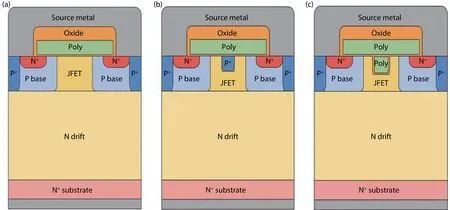
Fig.1.(Color online) Schematic cross-sectional structure of (a) C-MOSFET, (b) CI-MOSFET, and (c) DG-MOSFET.

Fig.2.(Color online) Proposed key fabrication process flow of DG-MOSFET.(a) Ion implantation to form the p-well and n+ source.(b) Dummy etching.(c) Dummy oxide deposition.(d) Nitride mask removal & poly-Si deposition.(e) Poly-Si etchback.(f) Gate oxidation and patterning.
3.Optimizing the structures
To analyze the performance of the proposed device, the compared devices were optimized.The CI-MOSFET and DGMOSFET were optimized based on the C-MOSFET.The drift thickness and concentration were fixed at 30μm and 1.7 ×1017cm−3, respectively.
3.1.Optimizing the C-MOSFET
Fig.3 shows the trade-off relationship betweenRONand BV based on the changes in the JFET width (WJF) and concentration (NJF).As shown,RONand BV decrease at the same time asWJFincreases.AsWJFincreases, the proportion of the depletion region in the JFET decreases.Therefore, the current path increases, thus decreasingRON.Meanwhile, the voltage concentrated in the p+region increases, which causes BV reduction.Baliga’s FOM (BV2/RON) was compared to optimize the C-MOSFET considering the trade-off betweenRONand BV, which is shown in Fig.4.WhenWJFis 3.5μm, the FOM is highest at allNJF.However,EMOXshould not exceed 4 MV/cm considering the reliability of the gate oxide[18].EMOXincreases with increasingNJF, which is more remarkable with increasingWJF.As a result, the C-MOSFET has the highest FOM whenNJFandWJFare, respectively, 3 × 1016cm−3and 3.5μm.In addition,EMOXdoes not exceed 4 MV/cm, and BV is greater than 3300 V.

Fig.3.(Color online) Influences of WJF and NJF of C-MOSFET.(a) The trade-off between RON and BV and (b) RON and EMOX (EMOX was measured at V S = 3300 V.).
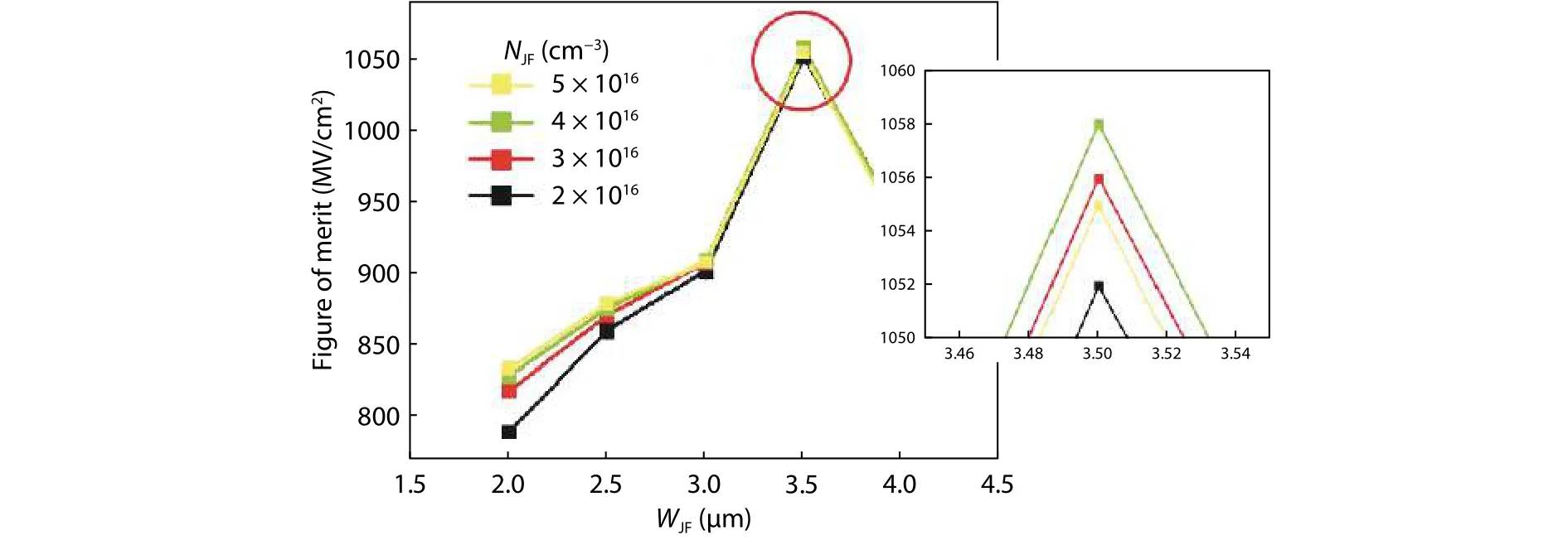
Fig.4.(Color online) Changes of FOM according to WJF and NJF of C-MOSFET.
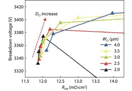
Fig.5.(Color online) The trade-off between RON and BV as variation of WCI and DCI.
3.2.Optimizing the CI-MOSFET
The BV,RON, and switching characteristics of the CI-MOSFET and DG-MOSFET are significantly affected by the CI and DG structures, respectively, existing under the gate.Therefore, the CI depth (DCI) and width (WCI) and the dummy depth (DDG) and width (WDG) were varied to optimize the two structures.As previously mentioned, both the structures were optimized based on the C-MOSFET.Therefore,WJFandNJFwere, respectively, fixed at 10μm and 3 × 1016cm−3, which were optimized for the C-MOSFET.
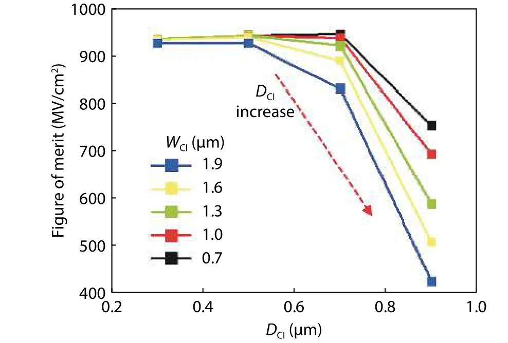
Fig.6.(Color online) FOM as a variation of WCI and DCI.
Fig.5 shows the trade-off betweenRONand BV of the CIMOSFET whenWCIandDCIare simultaneously varied.During the optimization process,DCIandWCIwere varied from 0.3 to 0.9μm and from 0.7 to 1.9μm, respectively.In Fig.5, at the sameWCI,RONincreases asDCIincreases.Moreover,RONincreases asWCIincreases at the sameDCI.This happens because the current path in the JFET decreases because of an increase in the CI region.In particular, asWCIincreases, the accumulation layer under the gate decreases, soRONincreases rapidly.However, the CI structure causes BV to increase by dis-persing the electric field concentrated in the p base.Therefore, to optimize the CI-MOSFET, it is necessary to compare the variation in the FOM based on the changes inWCIandDCI.In Fig.5, BV decreases rapidly whenDCIis 0.9μm.This happens because the electric field is concentrated in the CI structure whenDCIis too deep.This effect increases at lowerWCI.Therefore, the CI structure has the highest FOM whenDCI= 0.7μm andWCI= 0.7μm as specified in Fig.6.
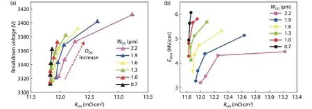
Fig.7.(Color online) Influences of WDG and DDG of DG-MOSFET.(a) Trade-off between RON and BV and (b) RON and EMOX (EMOX was measured at VDS = 3300 V.).

Fig.8.(Color online) Electric field distribution of three structures at VDS = 3300 V.(a) C-MOSFET.(b) CI-MOSFET.(c) DG-MOSFET.
3.3.Optimizing the DG-MOSFET
The DG-MOSFET was optimized in the same way as the CI-MOSFET.Fig.7 shows the result.The oxide thickness of the dummy region was fixed at 100 nm.As mentioned previously, the oxide in the dummy area was formed through a deposition process.
As shown in Fig.7,DDGandWDGare varied from 0.3 to 0.7μm and from 0.7 to 2.2μm, respectively.For the same reason as that for the CI-MOSFET, an increase in the dummy area increases bothRONand BV.Fig.7(b) shows the variations inEMOXandRONbased on the changes inWDGandDDG.EMOXincreases whenDDGincreases because of a decrease in the distance between the dummy oxide and the drain.In Fig.8, the vertex of the dummy has the highest electric field because of the electric crowding effect.This effect is alleviated with increasingWDGbecause the depletion region between the p base and the n drift protects the dummy oxide[19].Therefore,EMOXis reduced whenWDGincreases.However, as previously mentioned,RONincreases significantly because of the reduction in the current path.As a result,DDGandWDGwere optimized to 0.5 and 1.6μm, respectively.
4.Analysis of the electrical characteristics
4.1.Static characteristics
Based on the above results, we compared the performance of the three optimized structures.Fig.9 shows their blocking and output characteristics.The blocking characteristics were measured atVGS= 0 V, and the output characteristics were obtained atVGS= 20 V.Because of the source-contacted region in the JFET, the CI-MOSFET and DG-MOSFET have 16.2% and 15.2% higherRONthan C-MOFET, respectively.The BV values of the two structures are higher than that of the C-MOSFET because of the electric field dispersion effect.Table 1 lists the results of the static characteristics of the three optimized structures.The CI-MOSFET and DG-MOSFET have 10.4% and 11.5% lower static FOM than the C-MOSFET,respectively.
4.2.Dynamic characteristics
The static FOM values of the CI-MOSFET and DG-MOSFET deteriorate compared with that of the C-MOSFET.Nevertheless, both structures have improved switching characteristics.The increase inRONand the decrease in the switching power loss are in a trade-off relationship.Typically,RONis increased to reduce the switching power loss in high-frequency applications[20].
Fig.10 shows the input capacitance (CISS=CGS+CGD)and reverse transfer capacitance (CRSS=CGD) of the three structures with respect toVDSwhenVGS= 0 V[1,21].To extract the results shown in Fig.10, a low AC signal was applied at 1 MHz.A comparison of theCISSvalues of the three structuresshows that theCISSvalues of the CI-MOSFET and DG-MOSFET are significantly higher.This can be attributed to the presence of the source-contacted region (CI and DG) under the gate.Meanwhile, theCGDvalues of the CI-MOSFET and DGMOSFET significantly decreased.CGDis significantly influenced by the overlapping area between the gate and the drain.The DG-MOSFET can have a wider source-contacted area under the gate when it has a similar static FOM as that of the CI-MOSFET.Therefore, the DG-MOSFET has the lowestCGDbecause it has the smallest overlapping area between the gate and the drain.Therefore, the DG-MOSFET has 71%and 8.3% lowerCGDthan the C-MOSFET and CI-MOSFET.
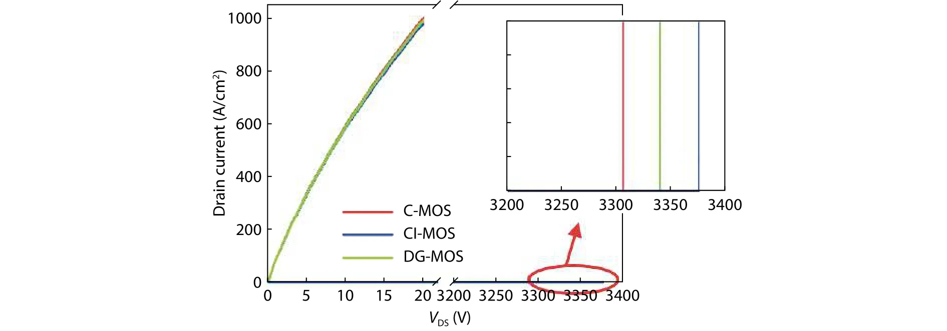
Fig.9.(Color online) Static characteristics of three structures.

Table 1. Static characteristics of the optimized three structures.

Fig.10.(Color online) Input and Gate-Drain capacitance of three structures.
Fig.11 shows the gate charge curves of the three structures.The test circuit is specified in Fig.11, and a current of 100 mA was applied to charge the gate.TheQGDvalue of the C-MOSFET is higher than those of the CI-MOSFET and DG-MOSFET.This happens becauseCGDis significantly reduced in both the structures.The HF-FOM values of the three structures were calculated and compared in Table 2.For the CIMOSFET and DG-MOSFET,RONincreased compared with that of C-MOSFET, butQGDdecreased significantly.As a result, the DG-MOSFET has a 59.2% lower HF-FOM than the C-MOSFET and 22.2% lower than the CI-MOSFET.
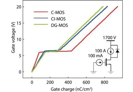
Fig.11.(Color online) Gate-drain charge curve of three structures.

Table 2. Capacitance and gate charge values of the three structures.
Fig.12 shows a diagram comparing the switching characteristics of the three structures through a double-pulse test simulation.Figs.12(a) and 12(b) show the turn-off and turnon transients, respectively.The test circuit is specified in Fig.12(a), and the load inductance and stray inductance are 400μH and 10 nH, respectively.
Consequently, the power losses in the DG-MOSFET and CI-MOSFET are significantly lower than those in the C-MOSFET.Table 3 lists the switching power loss during the doublepulse test.As listed, the DG-MOSFET has 53.4% and 5.5%lower total switching loss (ESW) than the C-MOSFET and CIMOSFET, respectively.
4.3.Power loss simulation
The power loss was compared using devices as switches in the power circuit through a PSIM simulation.Fig.13 shows the buck converter and boost converter circuits used in the power loss simulation.Both circuits comprise an RLC passive device, a diode, and a switch.The L and C components helpto remove the unnecessary ripple elements of the output voltage[22].The C-MOSFET, CI-MOSFET, and DG-MOSFET are used as switches in the power circuit.In consideration of the ideal gating block in the input gate voltage, the duty cycle was set to 0.5 and the frequency was set to 500 kHz.Finally,the output voltage was measured as the voltage of the load resistance.
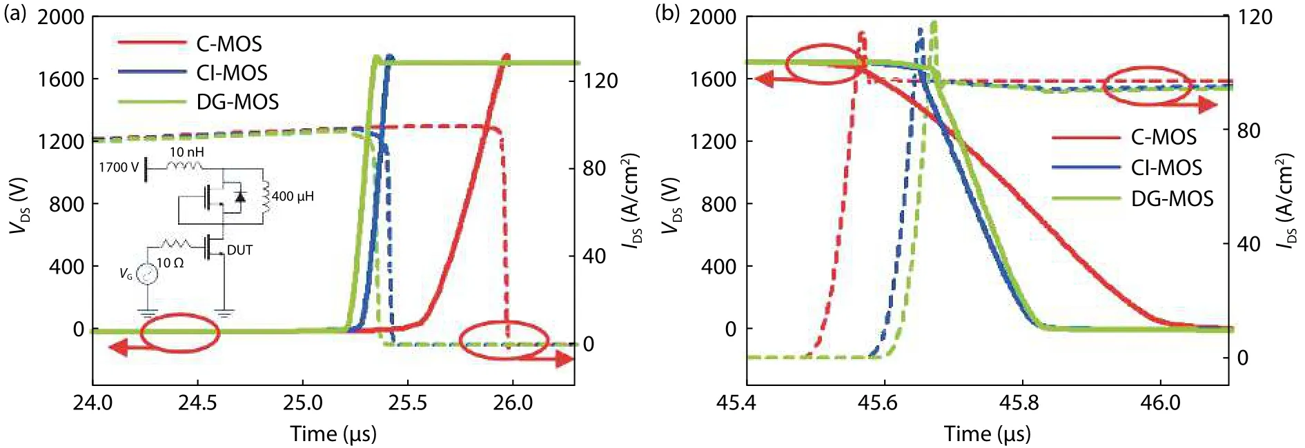
Fig.12.(Color online) (a) Turn off and (b) turn on transient of the three structures.

Fig.13.(a) Buck converter and (b) boost converter circuit used in the power loss simulation.
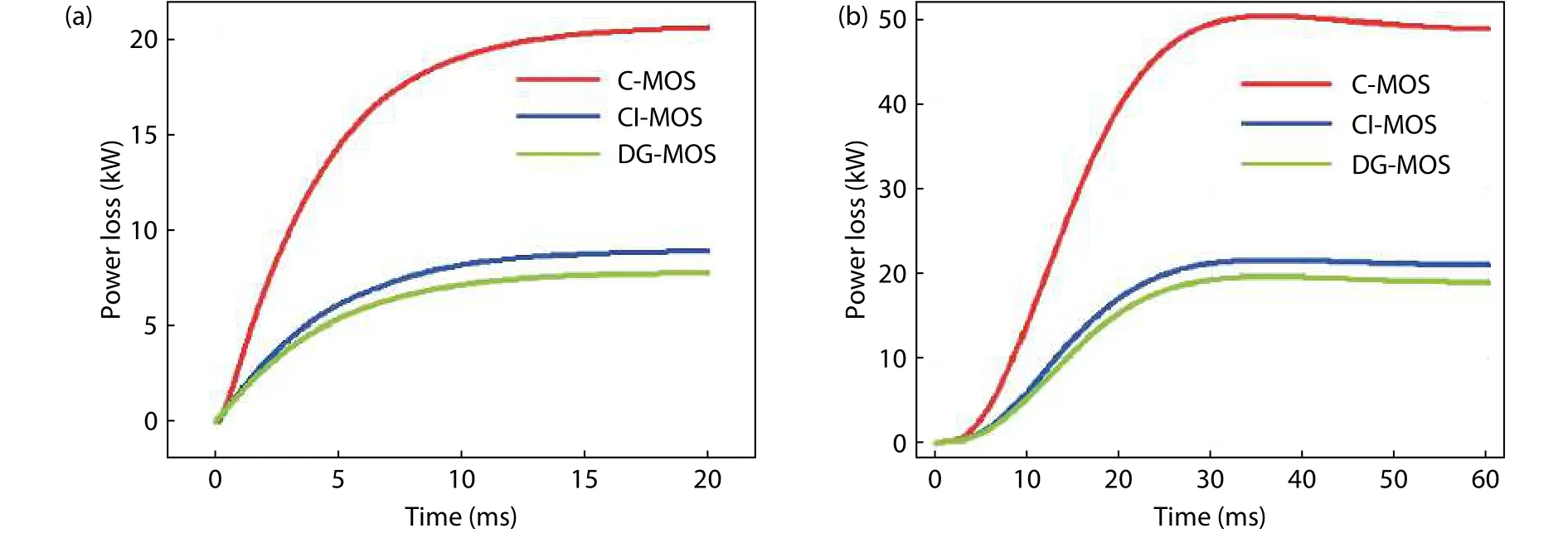
Fig.14.(Color online) Switching power loss in the power circuit.(a) Buck converter.(b) Boost converter.

Table 3. Double-pulse test simulation results.
Fig.14 shows the power loss simulation results.These results are specified in Table 4.They were recorded after each circuit reached a steady state.As mentioned previously, the DG-MOSFET has the leastPSW.Consequently, when the DG-MOSFET is used as a switch,PSWis improved by 61.9% and 12.7%compared with those of the C-MOSFET and CI-MOSFET in the buck converter.Likewise, in the boost converter,PSWis improved by 61% and 9.6%, respectively.

Table 4. Power simulation results (f = 500 kHz).
5.Conclusion
In this study, a 4H-SiC DMOSFET with a source-contacted dummy gate (DG-MOSFET) was developed and compared with the C-MOSFET and CI-MOSFET through TCAD and PSIM simulations.The simulation results confirmed that the pro-posed DG-MOSFET structure has the leastPSW.When applied to a power circuit, this structure could save 61% and 12%PSWin the buck converter and 61% and 9.6%PSWin the boost converter.In particular, the DG-MOSFET exhibited a lowerRONthan the CI-MOSFET.Consequently, it exhibited a lower HFFOM and a lower switching loss than the C-MOSFET and CIMOSFET.Thus, it can be concluded that the proposed DG-MOSFET is more suitable for high-frequency applications.
Acknowledgements
This research was supported by the MSIT (Ministry of Science and ICT), Korea, under the ITRC (Information Technology Research Center) support program (IITP-2020-2018-0-01421) supervised by the IITP (Institute for Information & Communications Technology Planning & Evaluation).
 Journal of Semiconductors2021年6期
- Journal of Semiconductors的其它文章
- L ow-bandgap Sn–Pb perovskite solar cells
- GIWAXS:A powerful tool for perovskite photovoltaics
- Dithieno[3',2':3,4;2'',3'':5,6]benzo[1,2-c][1,2,5]oxadiazole-based polymer donors with deep HOMO levels
- Efficient p-type doping in ultra-wide band-gap nitrides using non-equilibrium doping method
- Magnetic quantum oscillation in a monolayer insulator
- A review of manufacturing technologies for silicon carbide superjunction devices
