L ow-bandgap Sn–Pb perovskite solar cells
Rui He, Chuantian Zuo, Shengqiang Ren, , Dewei Zhao, , and Liming Ding,
1College of Materials Science and Engineering, Engineering Research Center of Alternative Energy Materials & Devices (MoE),
Sichuan University, Chengdu 610065, China
2Center for Excellence in Nanoscience (CAS), Key Laboratory of Nanosystem and Hierarchical Fabrication (CAS), National Center for Nanoscience and Technology, Beijing 100190, China
Record power conversion efficiency (PCE) for organic–inorganic halide perovskite solar cells (PSCs) has been rapidly boosted from 3.8% to 25.5%, approaching the Shockley–Queisser(S–Q) limit for single-junction solar cells[1−3].Multi-junction tandem solar cells provide a feasible approach to break the efficiency limit for single-junction solar cells by maximizing the use of the solar spectrum and photon energy.All-perovskite tandem solar cells have the advantages of tunable bandgaps,solution processability, and flexibility[4−6].As long-wavelengthlight absorbers, low-bandgap (Eg:~1.1–1.3 eV) perovskites play a vital role in making efficient all-perovskite tandem solar cells[7,8].Generally, low-Egperovskites are prepared by partially substituting lead (Pb2+) with tin (Sn2+)[9].However,mixed Sn–Pb perovskites usually suffer from short carrier lifetimes, high defect density, and easy oxidation of Sn2+[10].
To obtain high-quality Sn–Pb perovskite films and efficient low-EgPSCs, many efforts have been devoted in the past years.Zhaoet al.demonstrated an enhanced carrier lifetime up to ~250 ns in (FASnI3)0.6(MAPbI3)0.4(FA = formamidinium, MA = methylammonium) perovskite film with a bandgap of 1.25 eV by regulating its growth process.Improved crystallinity and enlarged grain size were obtained.The corresponding solar cells gave a certified PCE of ~17%[11].They further reduced the defects, suppressed the trap-assisted recombination, decreased the dark saturation-current density in thicker Sn–Pb perovskite filmsviachlorine or bromine doping, enhancing the PCEs to 18.1% and ~19%, respectively[12,13].This enables making two-terminal (2-T) tandem solar cells with a PCE of 21%.In early 2019, Zhuet al.got a PCE of 20.5% for single-junction low-EgPSCs by incorporating guanidinium thiocyanate (GuaSCN) into perovskite[8].GuaSCN greatly prolongs carrier lifetime to 1232 ns, which is almost ten times longer than that of the control one, resulting from reduced defect density in perovskite films.Tan group improved the efficiency of low-EgPSCs to 21.1% by adopting Sn powders to enable a comproportionation reaction of Sn and Sn4+and thus suppress the oxidation of Sn2+[14], delivering high-quality low-Egperovskite films with long charge carrier diffusion length(~3μm) and less defects.
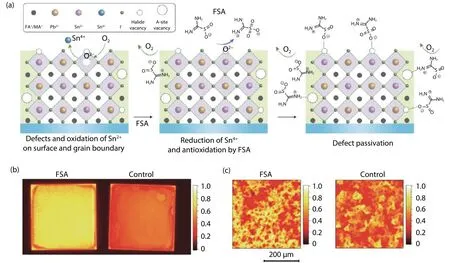
Tanet al.used a surface-anchoring zwitterionic antioxidant, formamidine sulfinic acid (FSA), to reduce Sn4+back to Sn2+and meanwhile passivate both electron-donating and electron-accepting defects on the grain surfaces (Fig.1(a))[15].They proposed that FSA can coordinate with perovskite precursorviadative bonding, resulting in delayed and more uniform crystallization due to the less volatile nature of FSA compared with DMSO.X-ray photoelectron spectroscopy (XPS) results indicated that Sn4+was reduced significantly.The enhanced photoluminescence (PL) intensity and prolonged carrier lifetime indicated decreased defect density.More importantly, the PL imaging for the films (Figs.1(b) and 1(c)) suggests that FSA significantly improved the uniformity of perovskite film.FSA-based PSCs gave PCEs of 21.7% and 18.8%for aperture areas of 0.049 and 1.05 cm2, respectively.
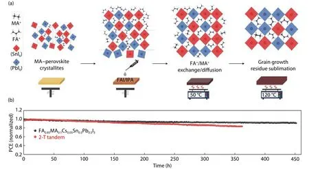
Though the efficiency of low-EgSn–Pb PSCs has been greatly improved, the relatively poor stability originating from volatile MA+inhibits the development of low-EgPSCs and their application in all-perovskite tandem solar cells.Liet al.designed a two-step bilayer interdiffusion growth method to reduce MA proportion in FA0.85MA0.1Cs0.05Sn0.5Pb0.5I3perovskite film[16].Methylammonium thiocyanate (MASCN) was added into SnI2/PbI2precursor, followed by spin-coating on PEDOT:PSS substrates, and then FAI solution in isopropanol(IPA) was spin-coated (Fig.2(a)).This two-step process could prolong the ion interdiffusion stage and slow down the crystallization.Moreover, Sn2+oxidation was suppressed, which benefits from the strong bonding between SCN–and Sn2+.The temperature-programmed desorption mass spectrometry (TPD-MS) results suggested that FA0.85MA0.1Cs0.05Sn0.5-Pb0.5I3has better thermal stability than one-step-processed(FASnI3)0.6(MAPbI3)0.4perovskite, which could be due to reduced MA content.
Time-of-flight secondary ion mass spectroscopy (TOF–SIMS) reveals that volatile MA+tends to accumulate at the film surface and evaporates under heating, leading to increased recombination center caused by MA+and I–vacancies and deterioration of device performance.Hence, they proposed a strategy to passivate the surface and grain boundaries by introducing one-dimensional (1D) PySnxPb1–xI3perovskite on surface of mixed Sn–Pb perovskite film[16].The photoluminescence (PL) was remarkably enhanced and the carrier lifetime was boosted from 670 to 1100 ns.Cross-sectional Kelvin probe force microscopy (KPFM) showed diminished electric-field difference at hole-transport layer (HTL)/perovskite interface and reinforced electric-field difference at perovskite/electron-transport layer (ETL) interface, further proving the surface passivation by PySnxPb1–xI3and improved junction quality.The PCE for 1.28 eV bandgap PSCs was improved to 20.4% with a high open-circuit voltage (Voc) of0.865 V.An encapsulated cell remained 92% of its original PCE after maximum power point (MPP) tracking for 450 h under continuous one-sun illumination, showing good operational stability (Fig.2(b)).

Fig.1.(Color online) (a) Schematic illustration of antioxidation and defect passivation by FSA at grain surfaces (including film surface and grain boundary) in mixed Pb–Sn perovskite films.A-site represents the site of monovalent cations.(b) PL imaging and (c) zoomed-in micro-PL mapping for the control and FSA-containing films on glass substrates (size 2.5 × 2.5 cm2).The colour bars stand for the normalized PL intensity.Reproduced with permission[15], Copyright 2020, Nature Publishing Group.

Fig.2.(Color online) (a) Schematic illustration for the two-step bilayer interdiffusion growth process.(b) Maximum power point (MPP) tracking on a FA0.85MA0.1Cs0.05Sn0.5Pb0.5I3 solar cell and a 2-T all-perovskite tandem solar cell with encapsulation measured in air under simulated AM 1.5G illumination.Reproduced with permission[16], Copyright 2020, Nature Publishing Group.
Additive engineering plays an important role in making high-quality low-Egperovskite films, but the underlying mechanisms are not fully understood yet.Herzet al.systematically investigated the effect of the commonly used SnF2additive on the structure and optoelectronic properties of FA0.83Cs0.17SnxPb1−xI3(0 ≤x≤ 1) perovskite films[17].Detailed XRD characterizations on the films with different Sn:Pb ratios and SnF2content indicated that SnF2improved the quality ofmixed Sn–Pb perovskite filmsviapreventing formation of Sn vacancies and associated lattice strain.Samples without SnF2exhibit significant tetragonal lattice distortion which can be greatly restrained by addition of SnF2.They also measured terahertz (THz) transmission spectra for the samples in dark to reveal the impact of Sn:Pb ratio and SnF2content.The background doping density caused by Sn oxidation in FA0.83Cs0.17SnxPb1−xI3films was obtained by THz conductivity spectra and optical-pump-THz-probe (OPTP) measurements.The decrease in background hole doping density with the SnF2incorporation suggested that Sn oxidation was suppressed.Overall, the role of SnF2additive in mixed Sn–Pb perovskite films is reducing the background hole densityviasuppressing Sn2+oxidation, thus prolonging carrier lifetimes, mitigating energetic disorder, and improving carrier mobilities.
To further develop mixed Sn–Pb perovskite films and devices, attentions should be paid to following aspects:(1) Preventing the oxidation of Sn2+to Sn4+, which could result in short carrier lifetimes, short carrier diffusion lengths, and high defect density[14].Better antioxidants and passivation materials are expected to eliminate the carrier recombination centers and make high-quality mixed Sn–Pb perovskite films[15].(2) Slowing down the crystallization by regulating the preparation process or additives.Rapid crystallization generally results in small grains, leading to increased defects at grain boundaries or in grains, limiting device performance.(3) Improving the operational stability.Suppressing Sn2+oxidation and reducing MA+content are beneficial for stability enhancement.(4) Developing suitable techniques to make large-area Sn-Pb perovskite films and devices, and all-perovskite solar modules with a tandem structure[18].
Acknowledgements
This work was supported by the National Key Research and Development Program of China (2019YFE0120000), the Science and Technology Program of Sichuan Province (2020JDJQ0030), and the Fundamental Research Funds for the Central Universities (YJ201955).L.Ding thanks the National Key Research and Development Program of China(2017YFA0206600) and the National Natural Science Foundation of China (51773045, 21772030, 51922032, 21961160720)for financial support.
 Journal of Semiconductors2021年6期
- Journal of Semiconductors的其它文章
- GIWAXS:A powerful tool for perovskite photovoltaics
- Dithieno[3',2':3,4;2'',3'':5,6]benzo[1,2-c][1,2,5]oxadiazole-based polymer donors with deep HOMO levels
- Efficient p-type doping in ultra-wide band-gap nitrides using non-equilibrium doping method
- Magnetic quantum oscillation in a monolayer insulator
- A review of manufacturing technologies for silicon carbide superjunction devices
- Modeling the photon counting and photoelectron counting characteristics of quanta image sensors
