A 3.3 kV 4H-SiC split gate MOSFET with a central implant region for superior trade-off between static and switching performance
Jongwoon Yoon and Kwangsoo Kim
Department of Electronic Engineering, Sogang University, Seoul 04107, Korea
Abstract: A split gate MOSFET (SG-MOSFET) is widely known for reducing the reverse transfer capacitance (CRSS).In a 3.3 kV class, the SG-MOSFET does not provide reliable operation due to the high gate oxide electric field.In addition to the poor static performance, the SG-MOSFET has issues such as the punch through and drain-induced barrier lowering (DIBL) caused by the high gate oxide electric field.As such, a 3.3 kV 4H-SiC split gate MOSFET with a grounded central implant region (SG-CIMOSFET) is proposed to resolve these issues and for achieving a superior trade-off between the static and switching performance.The SG-CIMOSFET has a significantly low on-resistance (RON) and maximum gate oxide field (EOX) due to the central implant region.A grounded central implant region significantly reduces the CRSS and gate drain charge (QGD) by partially screening the gate-to-drain capacitive coupling.Compared to a planar MOSFET, the SG MOSFET, central implant MOSFET (CIMOSFET), the SGCIMOSFET improve the RON×QGD by 83.7%, 72.4% and 44.5%, respectively.The results show that the device features not only the smallest switching energy loss but also the fastest switching time.
Key words: 4H-SiC; split gate; on-resistance; reverse transfer capacitance; switching energy loss; switching time
1.Introduction
Silicon carbide (SiC) is considered to be a promising candidate for power applications, thanks to its superior material properties[1].In particular, the SiC MOSFET has been proven to have lower switching time and loss compared to the Si insulated-gate bipolar transistor (IGBT)[2−4].Recently, many studies on the SiC trench MOSFET have been conducted to achieve small cell pitches and high channel mobility.Rohm proposed a double-trench MOSFET that applies a grounded p+region in the source region to disperse the electric field and achieve low on-resistance (RON)[5,6].However, a high electric field at the trench corner may lead to a reliability problem, which in turn makes it difficult to meet the required 3 MV/cm oxide reliability limit[7].In the 3.3 kV class, this problem becomes more pronounced and the channel resistance does not have a significant effect on the overall resistance due to the thick drift region.Compared to the trench MOSFETs, the simpler fabrication process and lower reverse transfer capacitance (CRSS) of the planar MOSFETs are more suitable for high voltage (3.3 kV or larger) and fast switching applications.
There are many approaches to reduce theCRSS(orQGD) in planar MOSFETs.The most widely known structure is the split gate MOSFET (SG-MOSFET), which splits the gate polysilicon to reduce the gate oxide capacitance (COX).The SG-MOSFET not only has inferior static characteristics compared to that of the planar MOSFET, but also has a problem that the electric field is concentrated in the gate corner.As a result, the concentrated electric field concentrated at the gate corner can lead to punch through problems[8].To resolve these issues,various structures using the split gate concept have been studied.Agarwalet al.[9]successfully manufactured a 2.3 kV class SG-MOSFET, but failed to meet the 3 MV/cm limit.Hanet al.[10]proposed a buffered-gate MOSFET (BG-MOSFET) to lower the oxide field.However, the BG-MOSFET features a long cell pitch and highRON.Vudumulaet al.[11]obtained dramatic reduction in theCRSSby introducing a shorted-dummy gate between the split gates.Although the shielding effect of the dummy gate led to an increased breakdown voltage (BV),the depletion region caused by the dummy gate led to a higherRONcompared to that of a typical SG-MOSFET.Cree reported a central implant MOSFET (CIMOSFET) in which a p-type implant region was introduced in the middle of the JFET region of a planar MOSFET[12,13].The CIMOSFET can significantly reduce the gate oxide field andCRSSby introducing a grounded central implant region.Furthermore, by increasing the drift concentration they were able to achieve a lowerRONcompared to that of a planar MOSFET.However, the grounded central implant region of the CIMOSFET may increase the parasitic input capacitance (CISS) and negatively affect the switching time.Therefore, it seems very difficult to improve both static and switching performance in the SG-MOSFET.Moreover, research on the SG-MOSFET structure has only been studied up to the 2.3 kV class, and it is not clear whether the split gate concept can be applied to the 3.3 kV class.
A novel 3.3 kV split gate MOSFET with a central implant region (SG-CIMOSFET) is proposed and analyzed in comparison with the planar MOSFET, SG-MOSFET and CIMOSFET.Because of the high drain bias voltage in the 3.3 kV class, the SG-MOSFET does not guarantee the 3 MV/cm oxide limit.In addition, the SG-MOSFET suffers from issues such as punch through and drain-induced barrier lowering (DIBL), which make it more difficult to design.However, the SG-CIMOSFETblocks the oxide electric field by introducing a central implant region in the JFET region and resolves all these issues of the SG-MOSFET.Like the CIMOSFET, the SG-CIMOSFET can significantly reduce theRONbecause of the high drift doping concentration.By applying the split gate structure and grounded central implant region, theCOXand bulk depletion capacitance (Cdep) of the SG-CIMOSFET are reduced simultaneously.In addition, the grounded central implant region partially screens the gate-to-drain capacitive coupling as seen in the CIMOSFET, resulting in the lowestCRSSin spite of the high drift concentration.Since the gate is not directly in contact with the central implant region, theCISScan be reduced significantly compared to that of the CIMOSFET.As a result, the SG-CIMOSFET has the best high frequency figure of merit(HF-FOM) in terms ofRON×QGD,RON×CRSS,RON×QGand achieving a superior switching time as well as switching loss.Thus,the SG-CIMOSFET boasts a superior trade-off between static and switching performance.

Fig.1.(Color online) Schematic cross-sectional views of the MOSFETs.(a) Planar MOSFET.(b) SG-MOSFET.(c) CIMOSFET.(d) SG-CIMOSFET.
2.Device structure and optimization
This study was conducted by the Sentaurus TCAD tool[14].The electron/hole continuity equations and the Poisson equations were solved using doping-dependent Shockley–Read–Hall (SRH) recombination, Auger recombination, inversion and accumulation layer mobility models, and Okuto-Crowell models[15,16].The mobility model contains incomplete ionization, high-field velocity saturation, and band narrowing models.
2.1.Device structure and features
Fig.1 shows the schematic cross-sectional views of the planar MOSFET, SG-MOSFET, CIMOSFET, and SG-CIMOSFET.In all device structures, the thickness of the 4H-SiC drift layer is 30μm and the gate oxide thickness is 50 nm.In order to suppress the current flow disturbance resulting from the central implant region in the CIMOSFET and SG-CIMOSFET, a current spreading layer (CSL) with a doping concentration of 2 ×1016cm–3is introduced in all structures.The channel length and doping concentration are 0.5μm and 2 × 1017cm–3, respectively.A fixed charge concentration of 1 × 1012cm–2is included at the SiC/SiO2interface for all devices.In the CIMOSFET and SG-CIMOSFET, the p+base and the central implant region is set to same depth to prevent additional mask consumption.The doping concentration of the central implant region is set to 5 × 1018cm–3.
2.2.Optimization of each structure
In this optimization process, the drift concentration of all structures starts at 2.2 × 1015cm–3to set BV of 3.3 kV in the planar MOSFET.Fig.2(a) shows the maximum oxide electric field (EOX) andRONchanges of the planar MOSFET according to the JFET width (WJFET).EOXis obtained atVDS= 3000 V andVGS= 0 V.As theWJFETdecreases, the JFET resistance component increases significantly resulting in a highRON.However, a largeWJFETinduces a highEOXas it enhances the shielding ability of the p-base.Therefore,WJFET= 2.5μm (the cell pitch is 10μm in all structures), which satisfies the 3 MV/cm oxide reliability limit, was adopted in the rest of the study.The relationship between theLsplitand device characteristics is shown in Fig.2(b).In Fig.2(b), whenLsplitis less than 0.4μm,EOXis obtained when breakdown occurs because BV is less than 3000 V.As theLsplitdecreases so does theQGD.This is due tothe decrease in the area between the gate and the drain.Simultaneously, the accumulation resistance increases and the field plate effect of the MOS structure decreases, leading to degradation in theRONand BV[17,18].Therefore, changes in theLsplitresults in a trade-off between the static and dynamic characteristics.The SG-MOSFET shows a high oxide field at allLsplitvalues due to its high drain bias voltage.Even if the gate does not protrude (when breakdown occurs atLsplit= 0μm),it shows 3.138 MV/cm ofEOX, which does not satisfy the 3 MV/cm limit.Furthermore, the electric field concentrated at the edge of the gate increases the depletion of the p-base region, which can result in punch through if it extends to the N+source region.Fig.3 shows the electron current density distribution when breakdown occurs in the SG-MOSFET.IfLsplitis less than 0.6μm, premature breakdown due to punch through occurs.On the other hand, whenLsplitis 0.6μm or more, the electric field is far away from the p-base and N-drift junction, and premature breakdown can be suppressed.But longLsplitcannot achieve a lowQGDcompared to the planar MOSFET (210.37 nC/cm2), and the purpose of the split gate is lost.To solve this punch through problem, a long channel can be considered[11].However, if the channel length is increased, theVTH,RON, cell pitch, andQGDall increase.As a result, the SG-MOSFET is not the best option in the 3.3 kV class for these given problems.The central implant region is a good solution to these problems.

Fig.2.(Color online) (a) EOX and RON changes of the planar MOSFET according to the WJFET, and (b) influence of the Lsplit on BV, RON, QGD and EOX in SG-MOSFET.BV is extracted at VGS = 0 V and IDS = 1 μA/cm2.

Fig.3.(Color online) Electron current density distribution when breakdown occurs in the SG-MOSFET (a) when Lsplit = 0.5 μm, and (b) when Lsplit =0.6 μm.
Considering static and switching characteristics, theLsplit= 0.3μm was chosen for SG-CIMOSFET and SG-MOSFET in the rest of the study.Fig.4(a) shows theRONand BV relation in the SG-CIMOSFET according to changes in the central implant width (WP) and height (HP).AsWPandHPincrease,the depletion region of the JFET region expands and theRONincreases.However, the central implant area under the oxide disperses the electric field along with the p-base, greatly reducing theEOXand increasing the BV.WhenHPis small, the electric field dispersion effect is weak in the central implant region, and impact ionization still occurs in the p-base region(Fig.4(b)).On the other hand, whenHPbecomes large(0.6μm or more), an excessive electric field is concentrated in the central implant region and impact ionization occurs only in the central implant region (Fig.4(c)).When theWPis 0.8μm andHPis 0.5μm, impact ionization occurs simultaneously in the p-base and the central implant region.In this way, the highest BV (3940 V) and BV2/RONof 1281.88 MW/cm2were obtained as shown in Fig.4(d).Introduction of the central implant region in the SG-CIMOSFET greatly reduces the maximum oxide field to less than 1.4 MV/cm in all the cases in Fig.5(a).As a result, punch through is suppressed in SGCIMOSFET.Therefore, the SG-CIMOSFET can apply a short channel length while suppressing punch through problems when compared to the SG-MOSFET.Fig.5(b) shows theQGDvariation with respect toWPandHP.As theWPandHPincrease,QGDbecomes smaller because of the depletion expansion.Notably, increasingWPhas a greater impact on the decrease ofQGDthan increasingHP.This is because the grounded central implant region partially screens the capacitive coupling between the gate and the drain asWPincreases.Detailed analysis of the capacitance and gate charge characteristics will be covered in the next section.Consequently, the lowestRON×QGDof 418.17 mΩ∙nC and BV2/RONof 1199.79 MW/cm2were obtained forWP= 0.8μm andHP= 0.6μm.However,this study chose to move forward withWP= 0.8μm andHP=0.5μm, which resulted in the best BV2/RONand had an adequately lowRON×QGDof 460.18 mΩ∙nC.CIMOSFET also adopted these parameters as it resulted in the best BV2/RON.The CIMOSFET was almost the same BV (3949 V) as the SG-CIMOSFET.However, it has a lowerRON(11.19 mΩ∙cm2) than the SGCIMOSFET (12.11 mΩ∙cm2) due to its accumulation layer resistance.After parameter optimization, the BV of the SG-CIMOSFET and CIMOSFET was set to 3.3 kV by adjusting the drift doping concentration (3 × 1015cm–3) in order to compare theRONof four devices in the 3.3 kV class.
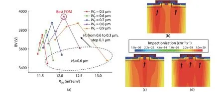
Fig.4.(Color online) (a) RON and BV relation in the SG-CIMOSFET according to change in WP and HP.(b)–(d) Impact ionization position when breakdown occurs in the SG-CIMOSFET according to change in WP and HP (the arrow indicates the breakdown point).
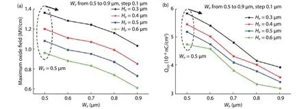
Fig.5.(a) EOX changes and (b) QGD changes in the SG-CIMOSFET according to change in WP and HP.EOX is obtained at VDS = 3000 V and VGS = 0 V.
3.Results and discussions
3.1.Static characteristics
Fig.6 shows theI–Vcharacteristics of four devices.RONis obtained forVGS= 20 V.BV is extracted atVGS= 0 V andIDS= 1μA/cm2.TheRONof planar MOSFET, SG-MOSFET, CIMOSFET,and SG-CIMOSFET are 10.39, 10.49, 8.59, and 8.67 mΩ∙cm2, respectively.Due to the increased drift doping concentration,CIMOSFET and SG-CIMOSFET were able to significantly improve theirRON.Also, the SG-CIMOSFET has nearly the sameRONas the CIMOSFET.This is because the current disturbance due to the accumulation resistance is minimized due to the improvement of the drift resistance, which occupies most of the total resistance.The off-state electric field distributions are shown in Fig.7.Due to the split gate structure of the SG-MOSFET, the electric field is concentrated on the gate edge (EOX=4.56 MV/cm) and thus the 3 MV/cm reliability limit cannot be met.However, due to the introduction of the central implant region, the electric field is dispersed in the SG-CIMOSFET, reducing theEOXby 2.5 times compared to the planar MOSFET and 4.3 times compared to the SG-MOSFET.CIMOSFET shows the lowestEOX(0.97 MV/cm) but is not significantly different from that of the SG-CIMOSFET (1.06 MV/cm).Fig.8 shows the band diagram in the channel of the four devices atVDS= 0 V(solid line) andVDS= 3000 V (dotted line).WhenVDS= 0 V,the band diagram of the four devices is nearly the same because of the same p-base and CSL doping concentration.However, the SG-MOSFET and planar MOSFET show the severe barrier lowering atVDS= 3000 V because of the potential around the channel resulting from the high electric field.The CIMOSFET and SG-CIMOSFET show excellent DIBL supp-ression due to the electric field shielding of the central implant region.
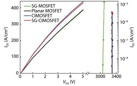
Fig.6.The I–V characteristics of the four devices.RON and saturation current is obtained for VGS = 20 V.BV is extracted at VGS = 0 V and IDS =1 μA/cm2.
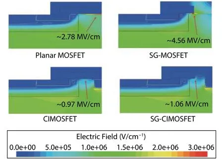
Fig.7.(Color online) Off-state electric field distributions of the four devices when VGS = 0 V and VDS = 3000 V.
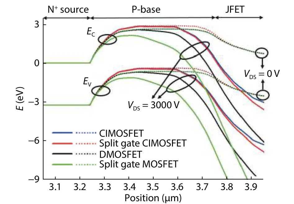
Fig.8.(Color online) The band diagram in the channel of the four devices at VDS = 0 V, VDS = 3000 V in off-state.
3.2.Capacitance and gate charge characteristics
For the analysis of the capacitance characteristics, the SG-CIMOSFET with floating central implant region is added to understand the capacitance characteristics.Fig.9 shows the capacitance characteristics as a function ofVDSfor the five devices.The CIMOSFET has the largestCISSdue to the overlap of the grounded central implant region and the gate.This in turn increases the switching time.In contrast, the SG-CIMOSFET shows a great reduction inCISScompared to the CIMOSFET, due to the separation of the central implant region and gate.In general, theCRSSis expressed by the following equation[8]:

whereCOXis the gate oxide capacitance andCdepis the bulk depletion capacitance.The SG-MOSFET reduces theCRSSby reducing theCOX.But at lowVDS, due to its shallow depletion region, the split gate structure induces a largeCdepcompared to that of the planar MOSFET, as shown in Fig.10(a)[8].Therefore, theCRSSof the SG-MOSFET temporarily becomes larger than theCRSSof the planar MOSFET in the vicinity ofVDS= 10 V, which is shown in the inset of Fig.9(a).The CIMOSFET reduces theCRSSin two ways.First,Cdepdecreases with the expansion of the depletion region of the bulk region.Second,the grounded central implant region under the gate screens the gate-to-drain capacitive coupling[19].CIMOSFET has lowCRSSdespite having shallow depletion regions in highVDS(Fig.10(b)) due to high drift doping concentration compared to SG-MOSFET and planar MOSFET.Therefore, screening the gate-to-drain capacitive coupling is the main reason forCRSSreduction.At a lowVDS, the floating SG-CIMOSFET and SG-CIMOSFET have lowerCRSSthan SG-MOSFET due to the wider depletion region by the central implant region as shown in Fig.10(a).On the other hand, at a highVDS, the floating SG-CIMOSFET exhibits slightly higherCRSSthan SG-MOSFET because of the large depletion region due to high drift doping concentration.But in SG-CIMOSFET, the grounded central implant region partially screens the gate-to-drain capacitive coupling like a CIMOSFET, resulting in the lowestCRSS.Therefore, as theWPincreases, the amount of screening gateto-drain capacitive coupling increases, resulting in a sharp decrease inQGDas shown in Fig.5(b).The drain source capacitance (CDS) characteristics of the five devices is shown in Fig.9(b).The grounded central implant region of the CIMOSFET and SG-CIMOSFET cause an increase inCDS.CDSof the floating SG-CIMOSFET is larger than that of SG-MOSFET and planar MOSFET.It is due to the shallow depletion region caused by the high drift concentration.As a result, the grounded central implant region converts part of theCRSStoCDSandCGSas shown in the capacitance model of the SG-CIMSOFET and the CIMOSFET (Fig.10(a))[20].Increases inCDSlead to an increase in output capacitance (COSS=CDS+CGD),which affects the reverse recovery characteristics of MOSFET due to the discharging current.However, the increase inCDSis not insignificant, and the effect of reducingCRSSis even greater.This further reduces the switching energy loss compared to SG-MOSFET.Detailed analysis of switching characteristics is shown in the next section.
The gate charge characteristics of the four devices are shown in Fig.11.The mixed-mode TCAD simulation circuit is shown in the inset of Fig.11.TheQGDis obtained by overlaying theVDSwaveform with the gate charge characteristic(measured at 90% of theVDSto 10% of theVDS)[21].The total gate charge (QG) is defined as the gate charge fromVGS= 0 V toVGS= 20 V.TheQG,QGD, andQTHvalues of the four devices are shown in Table 1.The SG-CIMOSFET has the lowestQGD(42.49 nC/cm2) andQG(424.85 nC/cm2).The CIMOSFET hasthe second highestQGD(77.21 nC/cm2) but has a higherQG(651.56 nC/cm2) than the SG-MOSFET (503.62 nC/cm2) due to its highCISS.Therefore, the SG-CIMOSFET features best characteristics in terms ofQG,QGD, andCRSS.In addition, it has the smallestQGD/QTHvalue, which helps to suppress the parasitic turn-on effect[21,22].The comprehensive performance of the four devices are shown in Table 1.The SG-CIMSOFET boasts the lowest HF-FOM in terms ofRON×QGD,RON×CRSS, andRON×QG.
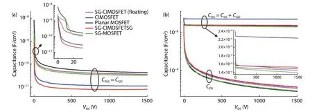
Fig.9.(Color online) (a) Reverse transfer capacitance characteristics (CRSS) of the five devices.(b) Input capacitance (CISS) and drain source capacitance (CDS) characteristics of the five devices (when VGS = 0 V, AC signal of 1 MHz).

Fig.10.(Color online) (a) Depletion lines and reverse transfer capacitance models of the five devices when VDS = 0 V, VGS = 0 V.(b) Depletion lines of the five devices when VDS = 800 V, VGS = 0 V.The solid black line represents the depletion layer.
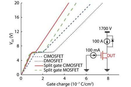
Fig.11.Gate charge characteristics and test circuit of the four devices.
3.3.Switching characteristics
The switching performance analysis of each device areconducted through a double pulse test (DPT) by the mixedmode TCAD simulation.The active areas of all devices under test (DUT) are set to 1 cm2.Fig.12 shows the switching waveforms of the four devices.The test circuit for DPT is shown in Fig.13(a).The body diode of the DUT was used as a freewheeling diode.The gate resistance and stray inductance are setto 20 Ω and 20 nH, respectively.The load inductor is set to 170μH and the firstVGSpulse lasted for 10μs to yield a load current of 100 A/cm2.The gate voltage is switched between 15 and –5 V.In this paper, the turn-off time (TOFF) consists of two parts, the turn-off delay time (TD-OFF:from 90% ofVGSto 10% ofVDS) and the turn-off fall time (TF:from 10% ofVDSto 90% ofVDS).The turn-on time (TON) consists of two parts, the turn-on delay time (TD-ON:from 10% ofVGSto 90% ofVDS) and the turn-on rise time (TR:from 90% ofVDSto 10% ofVDS)[23].Due to its lowCRSS, the SG-CIMOSFET shows the largest dV/dt, resulting in the fastest switching time in terms ofTOFFandTON.The CIMOSFET also shows fasterTFandTRcompared to the planar MOSFET and SG-MOSFET due to its lowCRSS.However, the CIMOSFET shows fairly slowTD-OFFandTD-ONdue to its highCISS.As a result, the CIMOSFET exhibitsTOFFandTONsimilar to that of the SG-MOSFET despite its lowCRSS.Fig.13(b) shows the switching energy loss diagrams of the four devices.Because the body diode of the DUT was used as a freewheeling diode,EONcontains the reverse recovery energy of the DUT.It shows theEONof the SG-CIMSOFET is much smaller than planar MOSFET and SG-MOSFET.This means that although grounded central implant region increases the reverse recovery energy, reduction of switching energy loss because of the reducedCRSSis more dominant in SG-CIMOSFET.The total switching energy loss (ETOTAL) of the SG-CIMOSFET decreased by 71%, 67%, and 22%, respectively,compared to the planar MOSFET, SG-MOSFET, and CIMOSFET.The comprehensive switching performance of the four devices is shown in Table 2.SG-CIMOSFET boasts the best switching performance in terms of switching energy loss and switching time.As a result, SG-CIMOSFET can achieve a superior trade-off between static and switching performance.
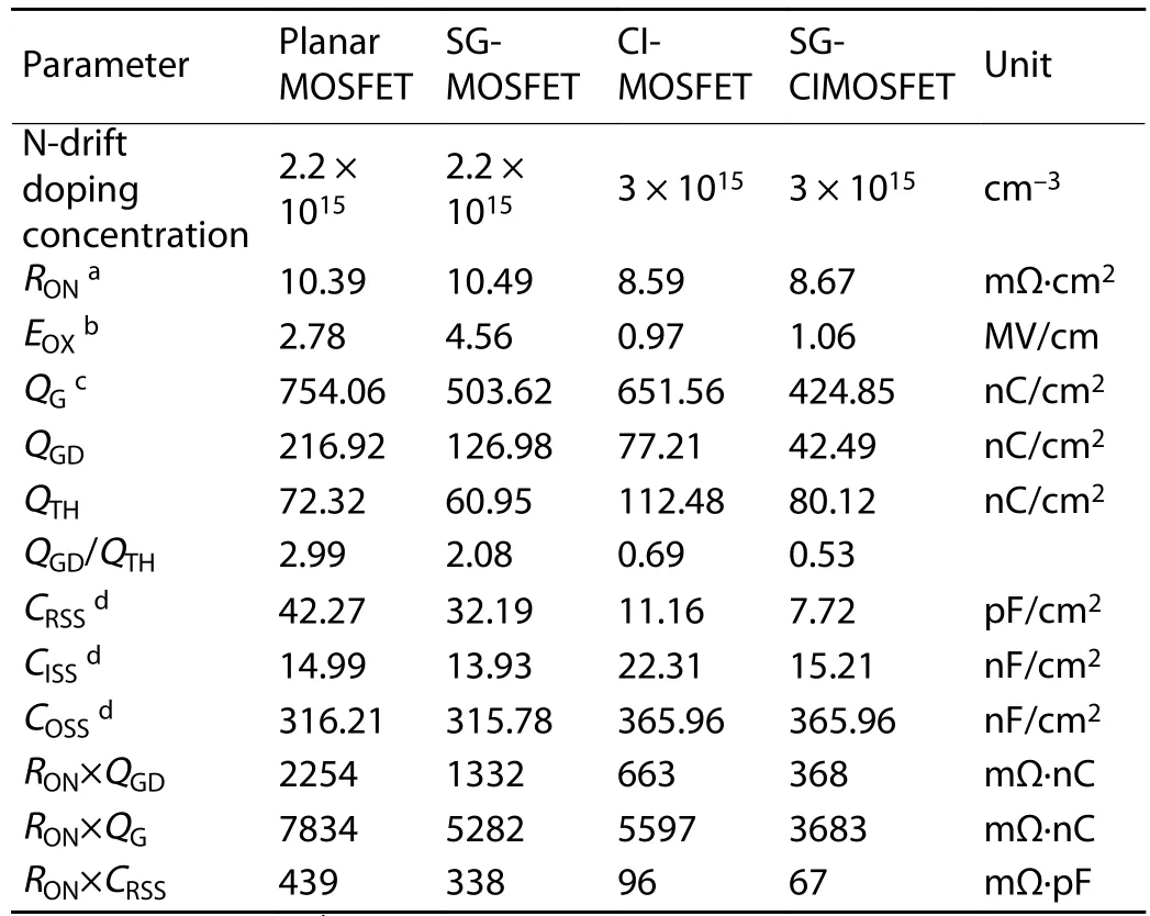
Table 1. Device characteristics comparison.
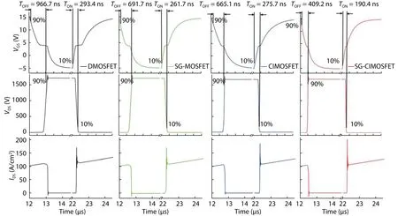
Fig.12.Switching waveforms of the four devices.The active areas of all DUT are set to 1 cm2.
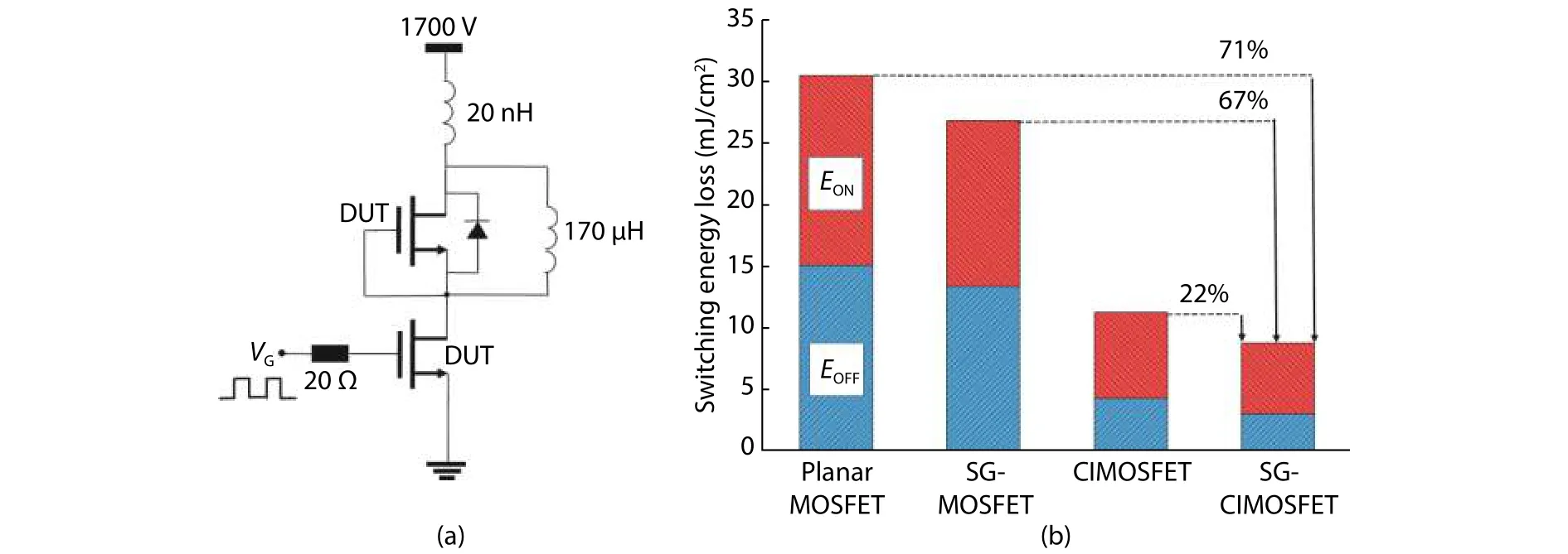
Fig.13.(Color online) (a) Double pulse test circuit.(b) Switching energy loss diagrams of the four devices.
4.Proposed fabrication process
Fig.14 shows the proposed fabrication procedure of SGCIMSOFET.After N-type epitaxial growth, the p-base and N+source region can be formed by ion implantation as shown in Fig.14(b).In Fig.4, it shows that the static characteristics of SG-CIMOSFET according toWPandHPare very sensitive.To minimize the sensitivity of parameters, tilt implantationcan be used to form the central implant region.TheWPandHPcan be determined by the implantation parameters[24].Since the P+base region and the central implant region are simultaneously formed by ion implantation, it is possible to prevent additional mask consumption as shown in Fig.14(c).The gate oxide with a thickness of 50 nm is formed by thermal oxidation.Then, polysilicon deposition and etching was carried out to form split gate structure.After ILD oxide deposition, the contact hole etching process followed to shorten the source and central implant region in Fig.14(g)[25].Lastly, the metallization process followed to form the source and drain contact.
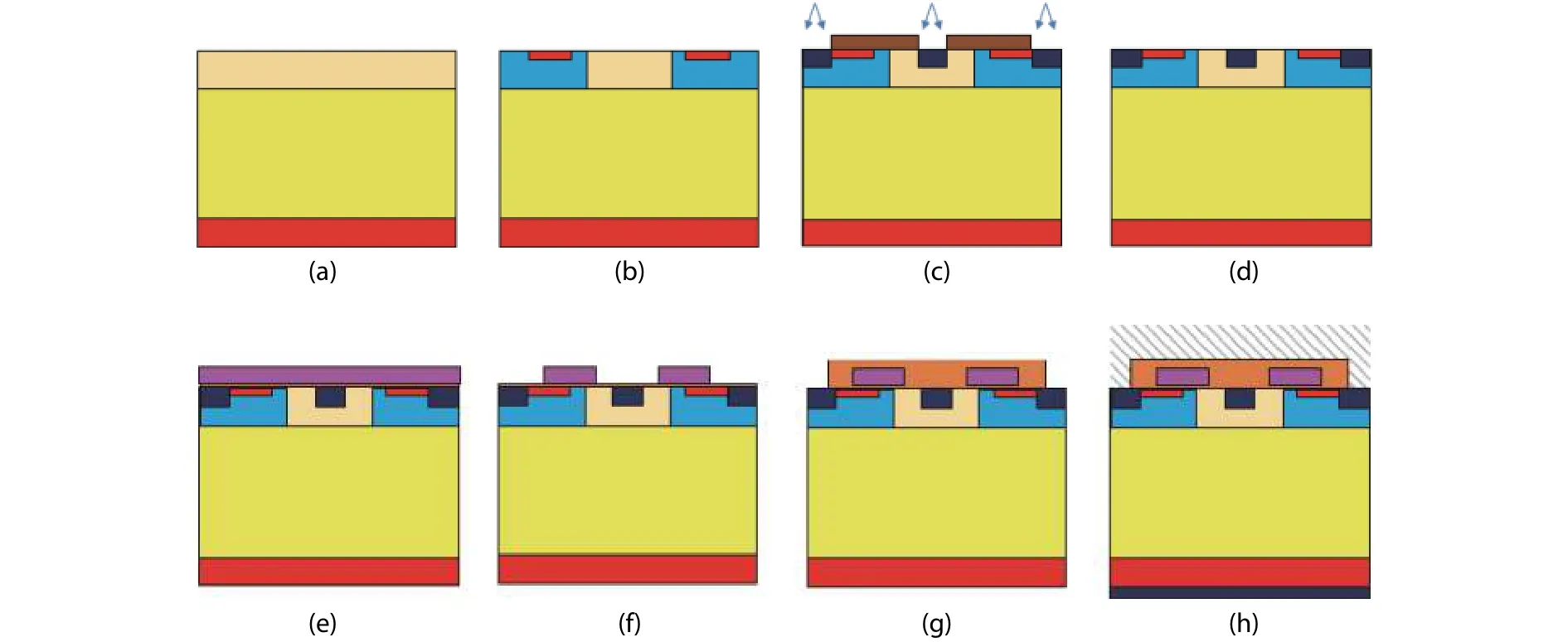
Fig.14.(Color online) Proposed fabrication procedure of SG-CIMSOFET.(a) N-type epitaxial growth.(b) Form the base and N+ source region.(c) Form the P+ base and central implant region by tilt ion implantation.(d) Thermal oxidation.(e) Polysilicon deposition.(f) Polysilicon etching.(g) ILD oxide deposition and contact hole etching.(h) Metallization to form the source and drain.
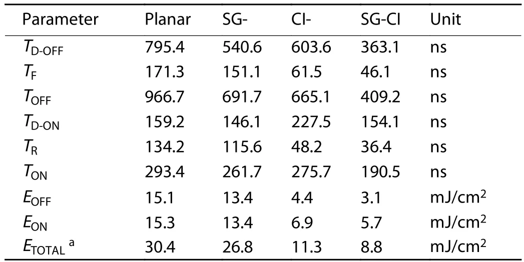
Table 2. Switching characteristics comparison.
5.Conclusion
In this paper, a novel 3.3 kV class 4H-SiC SG-CIMOSFET is proposed.In the 3.3 kV class, the SG-MOSFET does not guarantee reliable operation due to its high oxide electric field.Moreover, the SG-MOSFET is very vulnerable to the punch through and has been shown to suffer from severe DIBL effect, which makes it more difficult to design devices.The SGCIMOSFET resolves these problems by applying a central implant region and lowers theEOXby 4.3 times compared to SG-MOSFET.Furthermore, due to its increased drift doping concentration, the SG-CIMOSFET is able to significantly improveRON.In addition, the SG-CIMOSFET significantly lowers theCRSSby partially screening the gate-to-drain capacitive coupling.Compared to the planar MOSFET, the SG MOSFET and the CIMOSFET, the SG-CIMOSFET improves theRON×QGDby 83.7%, 72.4% and 44.5%, respectively.As a result, the SGCIMOSFET shows the best performance in terms of switching energy loss and switching time.In addition to its simple fabrication process, the SG-CIMOSFET boasts superior trade-off between static and switching performance, making it a promising candidate for high voltage and high frequency applications.
Acknowledgements
This research was supported by the MSIT (Ministry of Science and ICT), Korea, under the ITRC (Information Technology Research Center) support program (IITP-2020-2018-0-01421) supervised by the IITP (Institute for Information & communications Technology Promotion), and then Samsung Electronics.
 Journal of Semiconductors2021年6期
- Journal of Semiconductors的其它文章
- Oscillation neuron based on a low-variability threshold switching device for high-performance neuromorphic computing
- Determination of trap density-of-states distribution of nitrogendoped ultrananocrystalline diamond/hydrogenated amorphous carbon composite films
- 3.3 kV 4H-SiC DMOSFET with a source-contacted dummy gate for high-frequency applications
- Heavily doped silicon:A potential replacement of conventional plasmonic metals
- Modeling the photon counting and photoelectron counting characteristics of quanta image sensors
- A review of manufacturing technologies for silicon carbide superjunction devices
