Heavily doped silicon:A potential replacement of conventional plasmonic metals
Md.Omar Faruque, Rabiul Al Mahmud, and Rakibul Hasan Sagor
Islamic University of Technology (IUT), Board Bazar Gazipur, Gazipur 1704, Bangladesh
Abstract:The plasmonic property of heavily doped p-type silicon is studied here.Although most of the plasmonic devices use metal–insulator–metal (MIM) waveguide in order to support the propagation of surface plasmon polaritons (SPPs), metals that possess a number of challenges in loss management, polarization response, nanofabrication etc.On the other hand, heavily doped p-type silicon shows similar plasmonic properties like metals and also enables us to overcome the challenges possessed by metals.For numerical simulation, heavily doped p-silicon is mathematically modeled and the theoretically obtained relative permittivity is compared with the experimental value.A waveguide is formed with the p-silicon-air interface instead of the metal–air interface.Formation and propagation of SPPs similar to MIM waveguides are observed.
Key words: alternative plasmonic material; heavily doped p-silicon; surface plasmon polaritons
1.Introduction
Optical waveguide devices are making their way towards realizing low-cost high sensitivity and small-size devices, leading to many applications such as biological, environmental and chemical applications[1−3].Most of these waveguide devices use a metal-insulator-metal (MIM) waveguide to guide SPPs.Although metals such as gold and silver are mostly used in plasmonic devices due to their small ohmic losses and ability to confine light within considerable propagation length[4], at optical frequencies, metals suffer a huge optical loss due to interband transitions[5].Natural metals also have a large real part of its complex dielectric permittivity compared to dielectric, which causes a lot of problems in plasmonic devices that require a nearly balanced polarization response[6].Besides, the optical properties of metals degrade to a large extent when manufactured as thin films because metal films have different morphologies compared to a bulk metal[7].
To overcome the above-mentioned limitations of metals,another alternative material is proposed here which can support SPP propagation like natural metals.The plasmonic properties of natural metals can be described by its dielectric permittivity,ε, and magnetic permeability,μ.At optical frequencies, magnetic permeability,μ, is close to unity.Thus, the optical behavior can fully be described by the dielectric permittivity,ε[8].The complex dielectric permittivity of metals has a negative real part and a positive imaginary part.Both the real part and imaginary part is large in magnitude due to their high carrier concentration (≈1023cm–3).The large real part of the dielectric permittivity compared to the dielectric permittivity of the insulator causes an unbalanced polarization response in the MIM waveguide[9].Also, the large value of imaginary part is the reason for a comparatively higher optical loss.Thus, smaller values of both the real part and imaginary part of the dielectric permittivity of metal would have been advantageous for the plasmonic applications.
Silicon, when doped over a certain carrier concentration,shows negative real permittivity just like metals.Thus, it can support SPP propagation at its interface with a dielectric.So,it can be used to replace metals in the MIM structure.Both the real part and imaginary part of the permittivity depends on the carrier concentration which is tunable in this case of doped silicon and thus can be reduced to a certain limit to make the permittivity values smaller.Thus, both polarization management and optical loss can be controlled to a great extent.For the process of nanofabrication, silicon on insulator(SOI) is one of the key technologies nowadays.Since this kind of waveguide has only silicon in its structure, it can be treated in the same way as SOI structures.This will make the structure complementary metal oxide semiconductor (CMOS)-compatible and thus, will provide an easier way of fabrication.
2.Theoretical modeling of doped silicon
The p-silicon used here must be doped up to a certain carrier concentration in order to make it behave like metals.For our design, it is assumed to be doped in the range of 1020to 1021cm–3.Carrier concentration in this range has been practically shown by Shahzadet al.[9], Linaschkeet al.[10], Mizushimaet al.[11], Vinaet al.[12], Maet al.[13], Miyaoet al.[14]and Jellison Jret al.[15].The highest carrier concentration of 2 × 10²²in silicon has been reported by Nobiliet al.[16].The complex relative permittivity of highly doped silicon can be described by the Lorentz-Drude model[17].

If the real part and imaginary parts are separated, Eq.(1)becomes
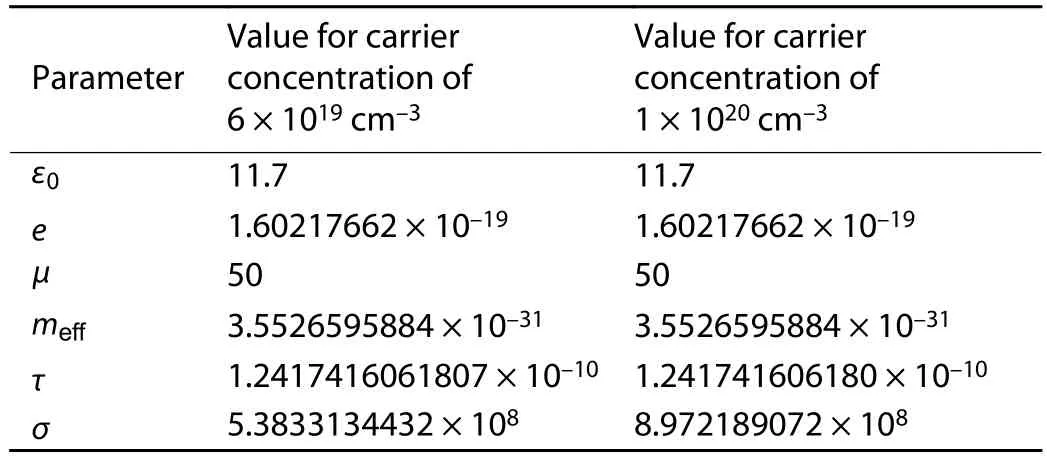
Table 1. Modelling parameters of heavily doped p-silicon by the Lorentz-Drude model.

whereωpis the plasma frequency,ε∞is the infinite frequency relative permittivity or the background permittivity,τis the electron/hole relaxation time,ω=2πc/λis the angular frequency,cis the speed of light in vacuum andiis the imaginary unit.In the case of the highly doped degenerate intrinsic semiconductors,ω2p=Ne2/ε0meffandτ=μmeff/e, whereNis the free carrier concentration,μis the electron/hole’s drift mobility andmeffis the averaged electron/hole effective mass[18].Usually, the angular frequencyω≫ωpandωτ≫1[19].Thus, Eq.(2) can be rewritten as

whereσ≈eNμis the conductivity of the doped silicon andeis the charge of an electron andε0is the free space permittivity.The infinite frequency relative permittivity or the background permittivity is the high-frequency limiting value that is approximately 11.7 for silicon and is independent of the doping concentration[20,21].Here,μ= 50[22]andmeff= 0.37m0,wherem0is the mass of the electron[23].The real part of the complex permittivity becomes negative after a certain concentration which can be calculated using Eq.(3).The values of different parameters of (3) for p-silicon carrier concentration of 6 × 10¹⁹and 1 × 1020cm–3is shown in Table 1.
The relative permittivity of heavily doped p-silicon has been experimentally measured by Shahzadet al.[9]for carrier concentration of 6 × 10¹⁹and 1 × 1020cm–3.Comparison between the values calculated from Eq.(3) and the experimental value for carrier concentration of 6 × 10¹⁹and 1 × 1020cm–3has been shown in Fig.1.
The percentages of error between the theoretically calculated value using the Lorentz-Drude model and the experimentally obtained value by Shahzadet al.at different wavelengths for p-silicon carrier concentration of 6 × 10¹⁹and 1 × 1020cm–3has been shown in Tables 2 and 3, respectively.
From Fig.1 and Table 2, it is observed that for a carrier concentration of 6 × 1019cm–3, the percentage of error between the theoretical value and the experimental value is very high (>160%) for wavelengths greater than 9.69μm,high (40%) for wavelengths between 6.5 to 9.69μm and very low (≤ 3.95%) for wavelengths less than 6.5μm.For a carrier concentration of 1 × 1020cm–3, the percentage of error is very high (>109.7%) for wavelengths greater than 26.23μm,high (20.35%–34.33%) for wavelengths between 3.86 to 17.69μm and low (≤ 7.12%) for wavelengths smaller than 3.34μm.
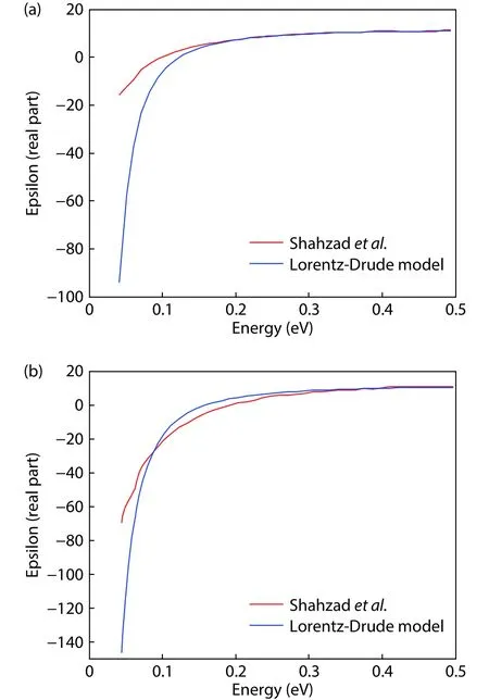
Fig.1.(Color online) Comparison between theoretical value and experimental value for carrier concentration of (a) 6 × 1019 cm–3 and (b) 1 ×1020 cm–3.
The Lorentz-Drude model mainly provides the frequency dependent dielectric permittivity of metals.In metals, electronic transition from the valence band to the conduction band takes place at a lower photon energy which is taken into consideration while theoretical modeling of any material is done using the Lorentz-Drude model.However, the band structure possessed by semiconductors like silicon is quite different compared to those of metals and the energy gap between the conduction band and valence band is also higher in semiconductors compared to metals.Thus, at lower photon energy, the dielectric property of doped silicon given by the Lorentz-Drude model, considering the contribution from interband transition of electrons, does not match with the experimental result as there is no interband transition practically.However, at higher photon energy, electrons in the semiconductor can absorb the required energy for interband transition just like metals.Thus, at higher photon energy, the Lorentz-Drude model can provide us with the more accurate values since the theoretical assumption regarding the interband transition also takes place practically.This difference in the theoretically predicted value and the experimentally obtained value at low photon energy has been depicted in Fig.1.At higher photon energy, the theoretical and experimental value matches with each other as predicted by the theory.Analyzing the data from Tables 2 and 3,it is evident that the model shows a low percentage of error for wavelengths smaller than 3.34μm.Thus, this model of heavily doped p-silicon can be used for the plasmonic devices, which work in the range of wavelengths smallerthan 3.34μm, which is the case for most of the plasmonic applications.

Table 2. Comparison of relative permittivity of p-silicon between the theoretical value and the experimental value for a carrier concentration of 6 × 1019 cm–3.

Table 3. Comparison of relative permittivity of p-silicon between the theoretical value and the experimental value for a carrier concentration of 1 × 1020 cm–3.
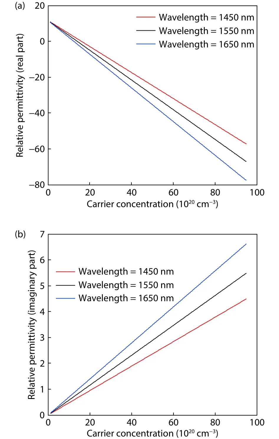
Fig.2.(Color online) Relative permittivity (a) real part and (b) imaginary part versus carrier concentration at different wavelength.
Heavily doped p-silicon can also be modeled at other carrier concentrations and wavelengths.The relationship of both the real part and imaginary part of the permittivity with carrier concentration and wavelength is almost linear.Fig.2 shows the plot of relative permittivity against carrier concentration for different wavelengths.
3.Comparison with conventional plasmonic metals
Among the conventional plasmonic materials, gold and silver are the most commonly used metals.A number of models for gold and silver are already available for use.The complex dielectric permittivity of gold and silver has been determined using both the Drude model and Lorentz-Drude model considering the effect of both free electrons and bound-electrons in metals.The part on which free-electron effects act, can be expressed in the following form:

and the part on which bound-electron effects act, can be described by the Lorentz model in the following form:

whereωprefers to the plasma frequency,krefers to the number of oscillation with resonance frequencyωn, dominant frequencyfn, damping frequencyΓnand1/Γnis the lifetime.HereΩprefers to the plasma frequency of the free-electronmodel having damping constantΓ0and oscillator strengthf0.Finally, the complex dielectric function can be described in the following form:

Table 4. Modelling parameters of gold and silver by the Drude and Lorentz-Drude model.
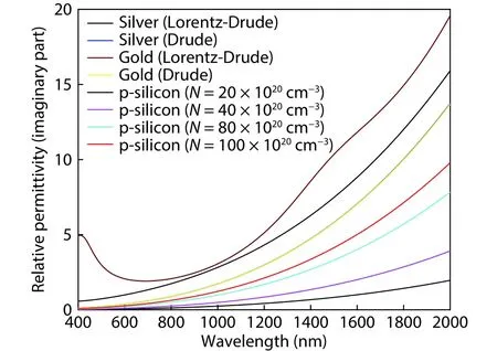
Fig.4.(Color online) Imaginary part of relative permittivity for silver and gold, and p-silicon for different values of carrier concentration.

Values of different parameters for obtaining the permittivity of gold and silver have been reported by Rakicet al.[24],which are shown in Table 4.
Since the relative permittivity is a complex quantity, it will have both real and imaginary parts.Fig.3 shows the real part of both gold and silver plotted along with the real part of the permittivity of p-silicon for different carrier concentration.

Fig.5.(Color online) Propagation of SPP along the silicon–air–silicon waveguide.
From Fig.3, it is observed that silver, gold and p-silicon,all have negative real parts of the permittivity after a certain wavelength.The real part of the complex permittivity for both gold and silver is larger than the p-silicon.This is mainly due to their high carrier concentration (≈1023cm–3).The large real part of the permittivity causes polarization mismatch in many plasmonic devices when the interface is created with an insulator[20,25,26].Thus, it is desirable to have smaller value of real permittivity for having a balanced polarization response.Since p-silicon has a comparatively smaller real part,it will be advantageous in forming plasmonic devices compared to both gold and silver.
Comparison between the imaginary parts of the dielectric permittivity is shown in Fig.4.The imaginary parts of the permittivity of both gold and silver are much larger than that of p-silicon even at a higher carrier concentration of p-silicon.Since the large value of the imaginary part is responsible for larger optical loss, plasmonic devices formed with p-silicon will suffer much lower optical loss than the conventional met-al plasmonic devices.
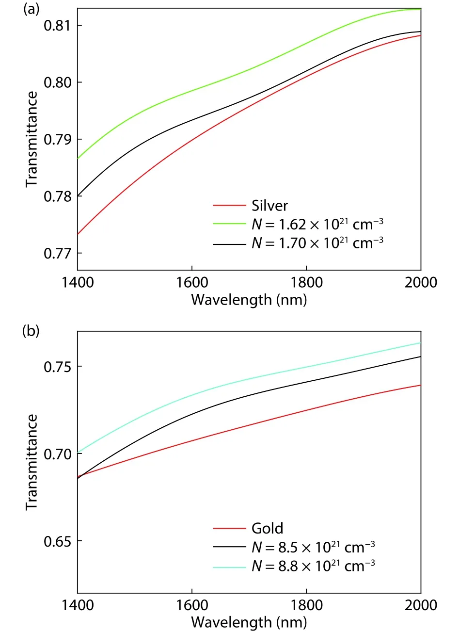
Fig.6.(Color online) Comparison of the transmittance between (a) the silver and p-silicon waveguide and (b) the gold and p-silicon waveguide.
4.Waveguide formation and result analysis
A straight waveguide with a ring resonator is formed with a silicon–insulator–silicon structure instead of MIM.The waveguide is simulated and SPP propagation similar to the MIM waveguide is observed.For simulation purposes, commercial simulation software COMSOL Multiphysics was used.Fig.5 shows the normalized electric field distribution at wavelength 1400 and 1800 nm respectively for the ring resonator structure formed with the silicon-air-silicon waveguide.From Fig.5, it is clearly observable that SPPs are created and propagated along the interface of p-silicon and air.Thus, we can come to a conclusion that p-silicon can be used as a replacement of metal in plasmonic devices in order to support SPP propagation.
The comparison of the transmittance in a straight waveguide formed with silver-air-silver and gold-air-gold with the same structure formed with a silicon-air-silicon waveguide with different carrier concentration is shown in Fig.6 which shows that, by doping the silicon up to a certain concentration, transmittance more than both the silver-air-silver and gold-air-gold can be achieved.The doped silicon waveguide can also be used to obtain transmission response of a notch filter similar to those of MIM waveguides by coupling the straight waveguide with a ring resonator as shown in Fig.5.The notch type response of the ring resonator structure with MIM waveguides and doped silicon waveguide is shown in Fig.7.The sensing characteristics of the ring resonator with doped silicon can be utilized to use it as a refractive index sensor by placing the sensing material in the ring waveguide.The resonant wavelength shifts with the change of refractive index,n, of the sensing material which is shown in Fig.8.Similarly, in most of the plasmonic devices, the metals like gold and silver can be replaced by doped silicon of the required carrier concentration to enhance the performance of the devices and to provide a more suitable way of fabrication.

Fig.7.(Color online) Notch type transmission response shown by ring resonators using gold, silver and psilicon.

Fig.8.(Color online) Sensing characteristics shown by ring resonators formed with heavily doped silicon.
5.Conclusion
A potential replacement of metals in plasmonic devices,heavily doped p-silicon is modeled here.The modeling parameters are found out for different carrier concentrations of p-silicon and the result is compared with the experimentally obtained result for the carrier concentration of 6 × 10¹⁹and 1 × 1020cm–3.In both cases, the error percentage for wavelengths smaller than 3.34μm has been found to be≤ 7.12% which trends to decrease gradually as the wavelength becomes smaller, since most of the plasmonic devices operate in the range of wavelengths smaller than 2μm where the error percentage is expected to be much less than the error obtained here.Thus, the mathematical model can be considered as verified one for wavelengths smaller than 3.34μm.The real part of the relative permittivity obtained in the model shows negative permittivity for a carrier concentration greater than 23 × 1020cm–3.Thus, it will behave like metal after doping with a carrier concentration of than 23 × 1020cm–3and can be used in plasmonic devices instead of metal to guide SPPs, which is also observed here by simulation.Hence, we can come to a conclusion that heavilydoped p-silicon can behave like metal and can be used as a replacement of metals in plasmonic devices which will help us to overcome optical loss, unbalanced polarization response and nanofabrication challenges possessed by metals.
 Journal of Semiconductors2021年6期
- Journal of Semiconductors的其它文章
- Oscillation neuron based on a low-variability threshold switching device for high-performance neuromorphic computing
- A 3.3 kV 4H-SiC split gate MOSFET with a central implant region for superior trade-off between static and switching performance
- Determination of trap density-of-states distribution of nitrogendoped ultrananocrystalline diamond/hydrogenated amorphous carbon composite films
- 3.3 kV 4H-SiC DMOSFET with a source-contacted dummy gate for high-frequency applications
- Modeling the photon counting and photoelectron counting characteristics of quanta image sensors
- A review of manufacturing technologies for silicon carbide superjunction devices
