Continuous-wave operation of InAs/InP quantum dot tunable external-cavity laser grown by metal-organic chemical vapor deposition*
Yan Wang(王岩), Shuai Luo(罗帅), Haiming Ji(季海铭), Di Qu(曲迪),2,†, and Yidong Huang(黄翊东)
1Innovation Center of Advanced Optoelectronic Chip,Institute for Electronics and Information Technology in Tianjin,Tsinghua University,Tianjin 300467,China
2Tianjin H-Chip Technology Group Corporation,Tianjin 300467,China
3Department of Electronic Engineering,Tsinghua University,Beijing 100084,China
4Key Laboratory of Semiconductor Materials Science,Institute of Semiconductors,Chinese Academy of Sciences,Beijing 100083,China
5Center of Materials Science and Optoelectronics Engineering,University of Chinese Academy of Sciences,Beijing 100049,China
Keywords: InAs/InP quantum dot,external-cavity laser,continuous-wave operation,metal-organic chemical vapor deposition
Broadband tunable light sources continually find new applications in a variety of scientific fields, in particular, environment monitoring[1]and optical fiber data communication based on wavelength division multiplexing(WDM) technology.[2]Self-assembled quantum dots (QDs)are promising for the next-generation light sources because of the unique random size distribution[3]and low state density[4,5]features. The two features of the QDs material mentioned above make it possible to be used on broad bandwidth tunable lasers under the low operating current.[6]Among several QD materials, InAs/GaAs QDs that lasing at around 1.3 μm wavelength have attracted the most attention,and many good performances have been achieved benefit from the high growth quality of epitaxial material.[7–11]However,InAs/GaAs QDs materials have difficulty reaching the window of 1.55 μm optical fiber telecommunication, and much attention has been shifted to InP/InAs QD materials.[12–21]Several growth technologies such as chemical beam epitaxy(CBE),[22]molecular beam epitaxy (MBE)[6], and metalorganic chemical vapor deposition(MOCVD)[16–19,23–25]have been developed to fabricate InAs/InP QDs. Compared with other methods,the MOCVD growth technique gets a lot of attention because it is a promising approach to meet the mass production requirements and an attractive substitution to the fine vacuum technology. However, in this technology, the growing temperature is so high that the As/P exchange would be exacerbated, which results in a large QD size fluctuation and a high defect density. These disadvantages hinder fabricating high-performance QD materials.[12,26]In order to overcome these difficulties, many different methods, such as the double cap (DC) procedure, have been introduced for QD growing, and the growth parameters have been elaborately optimized.[24,25]
Many different methods,such as changing the laser diode cavity length,varying the operation temperature,and employing the lasers as the active component of an external cavity(EC),have all been adopted to tune the wavelength of the laser.Among these methods, EC is the most popular one due to its low cost, outstanding performance, and simplicity characteristic. So far,many tunable external-cavity-lasers(ECLs)with telecommunication wavelength coverage[9,23,27–30]have been built on InAs/InP QDs materials, while most of the results have been limited to room temperature(RT)pulsed operation.As to the continuous-wave (CW) mode operation ECLs, the best result previously reported is 70 nm tuning ranges at RT with the QD lasers grown by GSMBE.[6]However,the results of CW working InAs/InP QD-ECLs grown by MOCVD have not been reported yet.
In this paper, we demonstrate a high-performance InAs/InP QDs structure grown by MOCVD for use in broadband tunable ECLs operating under CW mode at RT. The optical output characteristic and lasing spectrum of the F-P QDs laser was first investigated, which was performed with the laser cavity length of 1 mm under CW mode at RT. The center wavelength is around 1495 nm, and the 3-dB spectral bandwidth is approximately 10.8 nm, suggesting the capability on the applications of mode-locked laser for the broadband gain spectrum. Then the ECLs without facet coating are studied,and a 45 nm bandwidth ranging from 1480 nm to 1525 nm is realized. Last but not least,the dielectric coatings with AR(R ≈1%)and HR(R ≈85%)were respectively deposited on the front and back facets of a QD laser with 1 mm cavity length and the bandwidth tuning range expands from 45 nm to 92 nm which ranging from 1414 nm to 1506 nm. In most of the tuning range,the threshold current density is lower than 1.5 kA/cm2. The 6.5 mW maximum output power was obtained under a 500 mA injection current.
The InAs/InP QDs laser structure was deposited by an Aixtron 6×2 FT MOCVD system on a sulfur-doped InP(001)substrate. Phosphine (PH3), arsine (AsH3), triethylgallium(TEGa), and trimethylindium (TMIn), were prepared as the precursors. Figure 1(a)diagrammatically shows the sectional view of the QD laser. A 500 nm InP n-cladding layer and 200 nm lattice matching InGaAsP (1.15Q) waveguide were grown at 660◦C,and then the growth temperature was ramped down for the purpose of active region growth. The active region consisted of seven InAs stacked QDs separated by 30 nm 1.15Q spacing layers. The InAs layer was grown at the temperature of 470◦C with a deposition amount of 3.3 monolayers followed by the growth interruption of 5 seconds for indium full migration. Then the InGaAsP(1.15Q)were capped on the QDs,and the capping procedures can be separated into two steps. The growth temperature of the first capping layer was the same as the QD layer. Subsequently,the growth temperature was risen to 540◦C and sufficiently stabilized in the following 5 minutes under the atmosphere of phosphine. Then the second capping layer(SCL)was deposited on the substrate at a constant temperature of 540◦C. The growth procedure mentioned above was repeated for growing seven layers QDs.Finally, an InP p-cladding layer with a thickness of 1500 nm and an InGaAs contact layer with a thickness of 200 nm were grown. For device fabrication, a laser with the ridge waveguide of 6 μm was prepared through a standard photolithography technique and wet etching process. Au/Ge/Ni and Ti/Au alloys were used as n and p electrode separately. QD lasers with and without AR (R ≈1%)/HR (R ≈85%) cavity facet coating were both fabricated. The cavity length was 1 mm,and they were all fitted on the copper heat sinks p-side down for performance representation.
A schematic of the Littrow configuration ECLs system used in our experimental is represented in Fig. 1(b). The aspheric lens with numerical aperture (NA)=0.6 was used for collimating the light. The optical feedback was offered by a blazed grating with 600 grooves/mm through the first order diffraction. The length of the EC was about 15 cm. The bandwidth tuning was realized through the rotation of the grating to change the light incidence angle in order to pick out the EC resonant wavelength. The output power, optical spectra, and the bandwidth tuning performances mentioned above were all measured under CW mode at RT from the back facet of the QD lasers.

Fig.1. (a)Diagrammatic sketch cross-section proflie of the laser based on InAs/InP QDs material.(b)Schematic of the Littrow confgiuration externalcavity laser.
The AFM characterization presents the surface topography of the QDs,which are grown at the temperature of 470◦C with a deposition amount of 3.3 monolayers in Fig.2(a). The size of the measured area is 5×5 μm2. It can be obtained from Fig. 2(a) that the base height and diameter of the QDs are approximately 6±1 nm and 30±10 nm,respectively. No giant QDs appear on it, and the surface density of QDs is about 4.2×1010cm-2. The PL spectra of the QDs sample with seven stacked layers is shown in Fig.2(b). From the PL spectrum,it can be obtained that the wavelength of the active region is 1517 nm,and the full width half maximum is 153 nm(77 meV).
The optical output and volt-ampere characteristics of a 1 mm cavity length QD laser are shown in Fig.3. The test is performed under CW mode at RT without cavity facet coating.A 73 mA threshold current has been obtained, which corresponds to a 171 A/cm2threshold current density that is lower than the reported result.[11]The slope efficiency from the optical output plot for one facet is 0.106 W/A.Figure 3(b)presents the lasing spectrum for the 160 mA injection current.The center wavelength is around 1495 nm,and the 3-dB spectral bandwidth is approximately 10.8 nm,suggesting the capability on the applications of mode-locked laser for the broadband gain spectrum.
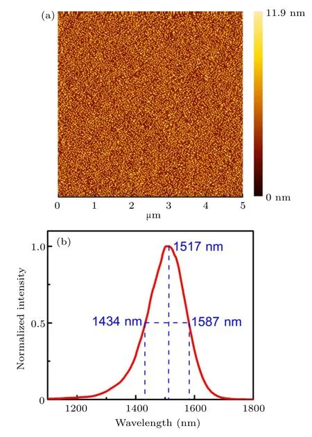
Fig.2. (a)AFM image of a 5 μm×5 μm InAs QDs grown at 470 ◦C with 3.3 MLs InAs supply. (b) PL spectra from the seven layers stacked QD sample.
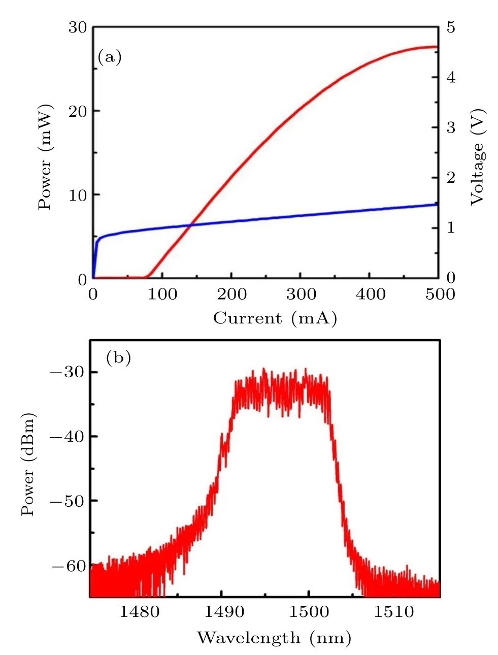
Fig. 3. (a) Optical output characteristics and (b) lasing spectra of the no facet coating QD lasers.
The QD laser without facet coating was also put into the Littrow system for obtaining the tuning performance. Figure 4(a) presents the normalized tuning spectra operated at 160 mA. For this device, a 45 nm tuning bandwidth ranging from 1480 nm to 1525 nm is received.
With the purpose of expanding the tuning range of the wavelength,AR with 1%reflectivity and HR with 85%reflectivity films were respectively deposited on the front and back cavity surface of a QD laser chip with the cavity length of 1 mm. The facet coating can effectively increase EC tuning ranges,which can be attributed to the effective suppression of FP resonance by AR facet coating and the reduction of optical loss by HR facet coating. As shown in Fig. 4(b), the bandwidth tuning spectra of the ECLs were measured under CW mode at 25◦C with a driving current of 180 mA. The tuning range width is 92 nm,which corresponds to the tuning wavelengths varying from 1414 nm to 1506 nm.
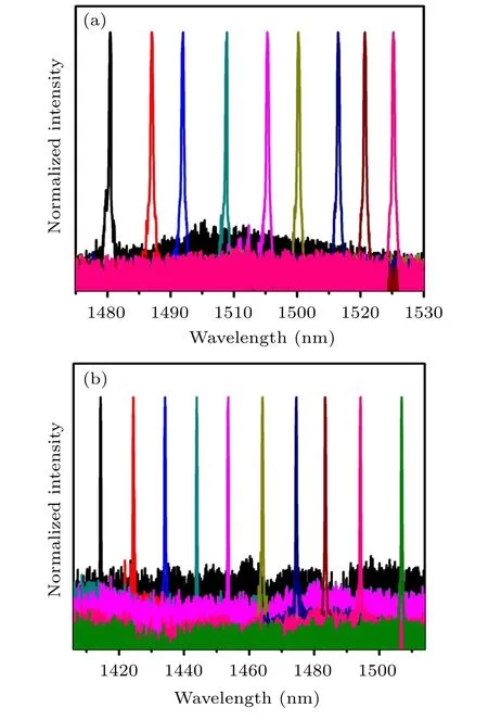
Fig.4. Tuning spectra of(a)no facet coating and(b)facet coating grating coupled ECLs with the active medium of InAs/InP QD.
As shown in Fig. 5(a), the threshold current density changes with wavelength tuning of the QD ECLs. The 66 nm tuning range (1424 nm–1490 nm) with no more than 100 mA bias (corresponding to the threshold current density of 1.5 kA/cm2)and 92 nm range(1414 nm–1506 nm)with no more than 220 mA bias (corresponding to the threshold current density of 3.3 kA/cm2) were obtained. For the ground state,due to the increment of cavity losses,the lowest threshold current(84 mA)is higher than the original uncoated laser threshold(75 mA).
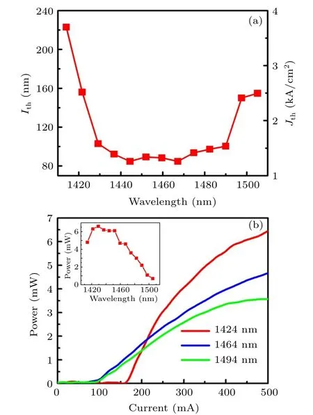
Fig. 5. (a) Dependence relationship between wavelength and threshold current density and (b) optical output curves of the facet coating ECLs for the wavelength of 1424 nm, 1464 nm, and 1494 nm. Under a 500 mA continuous injection current,the dependence relationship between the output power and lasing wavelength is shown in the inset of Fig.5(b).
Figure 5(b) shows the optical output curve of the ECLs with 1424 nm,1464 nm,and 1494 nm tuning wavelengths. As shown in Fig. S1 (supplementary materials), the wavelength of 1464 nm corresponds to the FP gain peak of the facet coating laser. The slope efficiency of the laser decreased when the wavelength was tuned toward the red shift side from the gain peak of 1464 nm. This can be mainly attributed to the finite state density at the red shift side,which leads to the low carrier capture efficiency. By contrast,large maximum output power and high slope efficiency were obtained when the wavelength was tuned toward the blue shift side from the gain peak,which is mainly resulted from the large state density. At the 1424 nm wavelength, a more than 6.5 mW maximum output power is acquired. The values of output power change with the tuning wavelength at a fixed 500 mA driving current were shown in the inset of Fig.5(b). The output power is measured from the HR coated cavity facet, and the maximum value of 6.5 mW was obtained.
In summary, we have exhibited a high-performance MOCVD grown InAs/InP QD structure for use in broadband tunable ECLs operating in CW mode at RT. Without cavity facet coatings, a 45 nm tuning bandwidth ranges from 1480 nm to 1525 nm is obtained under CW mode at RT.While combined with AR/HR facet coatings, a 92 nm tuning bandwidth range from 1414 nm to 1506 nm has been obtained.Within most of the tuning range, the threshold current density is less than 1.5 kA/cm2. The maximum power output of 6.5 mW is achieved at the wavelength of 1424 nm under a 500 mA injection current.
- Chinese Physics B的其它文章
- Numerical simulation on ionic wind in circular channels*
- Interaction properties of solitons for a couple of nonlinear evolution equations
- Enhancement of multiatom non-classical correlations and quantum state transfer in atom–cavity–fiber system*
- Protein–protein docking with interface residue restraints*
- Effect of interaction between loop bases and ions on stability of G-quadruplex DNA*
- Retrieval of multiple scattering contrast from x-ray analyzer-based imaging*

