
Self-powered solar-blind photodiodes based on EFG-grown(100)-dominant β-Ga2O3 substrate*
2021-01-21 02:08XuLongChu褚旭龙ZengLiu刘增YuSongZhi支钰崧YuanYuanLiu刘媛媛ShaoHuiZhang张少辉ChaoWu吴超AngGao高昂PeiGangLi李培刚DaoYouGuo郭道友ZhenPingWu吴真平andWeiHuaTang唐为华
Chinese Physics B 2021年1期
关键词:高昂
Xu-Long Chu(褚旭龙), Zeng Liu(刘增), Yu-Song Zhi(支钰崧), Yuan-Yuan Liu(刘媛媛),Shao-Hui Zhang(张少辉), Chao Wu(吴超), Ang Gao(高昂), Pei-Gang Li(李培刚),†,Dao-You Guo(郭道友), Zhen-Ping Wu(吴真平), and Wei-Hua Tang(唐为华),9,‡
1Laboratory of Information Functional Materials and Devices,School of Science&State Key Laboratory of Information Photonics and Optical Communications,Beijing University of Posts and Telecommunications,Beijing 100876,China
2Center of Materials Science and Optoelectronics Engineering,University of Chinese Academy of Sciences,Beijing 100049,China
3The Engineering Research Center for Semiconductor Integrated Technology,Institute of Semiconductors,Chinese Academy of Sciences,Beijing 100083,China
4China Aerospace System Simulation Technology Co.,Ltd. (Beijing),Beijing 100195,China
5Division of Interdisciplinary and Comprehensive Research&Platform for Characterization and Test,Suzhou Institute of Nano-Tech and Nano-Bionics,Chinese Academy of Sciences,Suzhou 215123,China
6Center for Optoelectronics Materials and Devices&Key Laboratory of Optical Field Manipulation of Zhejiang Province,Department of Physics,Zhejiang Sci-Tech University,Hangzhou 310018,China
7School of Nano-Tech and Nano-Bionics,University of Science and Technology of China,Hefei 230026,China
8College of Electronic and Optical Engineering&College of Microelectronics,Nanjing University of Posts and Telecommunications,Nanjing 210046,China
9National and Local Joint Engineering Laboratory for RF Integration and Micro-Packing Technologies,Nanjing University of Posts and Telecommunications,Nanjing 210046,China
Keywords: β-Ga2O3 substrate,Schottky photodiode,solar-blind detection
1. Introduction
The β-phase gallium oxide (β-Ga2O3) is most chemical and thermal stable among its five phases of α, β, ε, δ,and γ.[1–3]Owing to its high breakdown electric field (Ebr~8 MV/cm) and wide direct band gap (Eg~4.9 eV) responding in the ultraviolet(UV)solar-blind region,β-Ga2O3is extensively employed to construct the solar-blind photodetectors with various device structures,[3–6]including the typical metal–semiconductor–metal (MSM), p–n junctions, heterojunctions, and Schottky junctions structures, exhibiting many decent optoelectrical characteristics.
Thereinto,the junction-based devices may provide many promising device characteristics caused by the dispersive energy-band edges. In comparison, the heterojunctions with large enough band offsets are always good candidates for fabricating devices,while the two(or more)layers in heterojunctions need to be deposited at high temperatures and ultrahighvacuum conditions, translating to complex technologies and high costs, so the metals with high work functions contacting onto the semiconductor seem to be easier and cheaper.The Schottky-type photodetectors may well be more captivating due to the low dark current, fast response speed, and low noise performances, contributed by the constraint of carriers across the interfaces of the Schottky junctions.[7–11]As referenced by the reported papers, owing to the separation of electron–hole pairs in the Au/β-Ga2O3Schottky junction,an energy-saving self-powered device was achieved,showing a very low dark current of ~10-11A and a short response time of 64 μs.[10]A graphene/β-Ga2O3Schottky photodetector was fabricated and showed a high photo-responsivity of 29.8 A/W, a photo-to-dark current ratio of ~106, and a detectivity of ~1012Jones.[12]Thanks to the construction of built-in electrical filed at the interface between Ni and β-Ga2O3, a self-powered β-Ga2O3photodiode was developed by sputtering equipment and showed stable operation,[13]in which the high photo-responsivity of 144 A/W (10 V) was displayed. Moreover, a metal–oxide–semiconductor (MOS)-structured photodiode presented more desired performances for solar-blind photodetection, including self-powered operation and high external quantum efficiency.[14]
In consideration of the advantages of Schottky photodiode in performing solar-blind detection,we constructed Schottky diode photodetectors based on the edge-defined-film-fed(EFG)-grown (100)-dominated β-Ga2O3substrate, by using conventional UV photolithography, electron beam evaporation, and lift-off techniques. The breakdown and the solarblind photodetection were tested. The self-powered operation without any external energy apply (at zero bias) was further discussed.
2. Experimental details
Firstly, the 10 mm×10 mm β-Ga2O3substrate was grown by the EFG method.[15]The x-ray diffraction (XRD)was performed to verify the quality of the β-Ga2O3substrate.To fabricate the Schottky photodiodes, the conventional standard photolithography and lift-off technique were performed.The Ti/Au (30 nm/60 nm) and Ni/Au (30 nm/60 nm) were patterned by electron beam evaporation, serving as Ohmic and Schottky electrodes, respectively. The electron pattern is 400 μm wide and 600 μm long with 4 μm spacing distance,so the effective UV illuminated area of the fabricated device is calculated to be 4×600 μm2.
For characterizing the performances of the Schottky solar-blind photodiodes, the voltage–current (I–V) and timedependent current(I–t)measurements were carried out by using a Keithley 4200 semiconductor analyzer in air at room temperature (22.4◦C) in our lab. For the illuminated optoelectrical behaviors,a UV lamp that could emit 254 nm wavelength light was used, the distance between the measuring samples and the UV light source could be tuned to change the incident light intensity upon the surface of the samples.
3. Results and discussion
Using a single crystal XRD measuring equipment,the β-Ga2O3substrate sample was measured, the results show that the lattice parameters are a=12.22 ˚A,b=3.04 ˚A,c=5.80 ˚A,α=90◦,β =103.88◦,and γ=90◦. In Fig.1,the XRD shows the(400),(600),(800),and(002)peaks for the β-Ga2O3,suggesting a polycrystalline β-Ga2O3substrate used in this work.The 10 mm×10 mm β-Ga2O3substrate is shown in the inset of Fig.1.
We constructed 16 Schottky diodes on the 10 mm×10 mm β-Ga2O3substrate in this study. As presented in Fig. 2(a), all the Schottky diodes exhibit good rectified behaviors due to the asymmetric Ti and Ni metal electrodes.In Fig. 2(b), the I–V performances of the β-Ga2O3Schottky diodes in the dark and under illumination with light intensity of 100 μW·cm-2are displayed. Clearly, the rectified ratio of the device is 7.58×10⁴at±5 V.In addition,the reverse leakage current of the device is as low as 8.47 nA in the dark at a reverse bias of-5 V.The photo-to-dark current ratio(PDCR)is ~68.8 at -5 V responding to the 254 nm UV light with intensity of 100 μW·cm-2. For the diode device in this work,the Ohmic contact at the Ti/β-Ga2O3side could be referenced by electron tunnelling,[16,17]while the Schottky contact at the Ni/β-Ga2O3side is usually described according to the thermal electron(TE)model[17]

where I0is the reverse saturation current, A is the effective metal–semiconductor(M–S)contacted area,A*is the effective Richardson constant, n is the ideal factor, k is the Boltzmann constant, and φBis the Schottky barrier height (SBH). Here,A*is 41.1 A/cm2·K2,and is always expressed as[17]
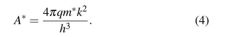
For Ga2O3, m*is taken as 0.342m0, where m0is the mass of free electron.[18]For the two devices,the spacing distance(L)between Ti/Au and Ni/Au is 4 μm,the area of the electron pattern is 3.6×104μm2. Therefore,the SBH can be calculated to be 0.67 eV for the device,based on Eqs.(1)–(4). In addition,the ideality factor n is estimated to be 1.72 for the device, in the range from 1 to 2,indicating a desired behavior of Schottky diode.

Fig.1. The XRD pattern of the EFG-grown β-Ga2O3 crystal substrate(shown in the inset).
Three selected Schottky diode samples from the fabricated devices were tested breakdown in air at room temperature (22.4◦C), suggesting that the breakdown voltages are 46.8 V,49.6 V and 50 V,as presented in Fig.2(c). Except for the different device scales,the low breakdown voltages in this report may be due to the inferior quality of the crystal. The improvement of the crystal quality could promote the higher breakdown voltages.[19–22]The work functions of Ti (Φ(Ti))and Ni(Φ(Ni))are 4.33 eV and 5.15 eV,respectively.[23]And the electron affinity of β-Ga2O3(χ(β-Ga2O3)) is 4.00 eV as reported in Ref. [24]. According to the Schottky–Mott rule,[25]the theoretical M–S interfacial barriers are 0.33 eV and 1.15 eV, for the Ti/β-Ga2O3and Ni/β-Ga2O3interfaces,respectively, as displayed in Fig. 2(d). Such asymmetric barriers contribute to the rectified effects of the Schottky diodes in this work,indicating the on-state at forward biases and offstate at reverse biases. The quite different results(great varies in reverse leakage currents)in Fig.2(a)may be due to the not very uniform surface of the β-Ga2O3substrate and/or the inconformity in micromachining processes. Under illumination,the electron–hole pairs are photo-generated,the absorbance of the incident photons(hv >Eg)could happen via the excitation of the electrons from the valence band edge to the conduction band edge of the β-Ga2O3substrate.

Fig.2. (a)The semi-log scale current–voltage characterizations of the 16 β-Ga2O3-based Schottky photodiodes on the 10 mm×10 mm substrate,(b) the semi-log scale current–voltage curves of the β-Ga2O3-based Schottky photodiode in the dark and under illumination with intensity of 100 μW·cm-2,(c)the breakdown of three selected device samples,(d)the energy-band diagram of the β-Ga2O3-based Schottky photodiode.
For the Schottky photodiodes in this study, the built-in electrical field (Ebuilt-in) is developed when the Ni and β-Ga2O3contact, owing to the interfacial barrier caused by the energy band bending at the edge of the conduction band(EC)(as shown in Fig.2(d)),leading to the rectified effects,as given in Fig.2(a). The electron–hole pairs are effectively separated by Ebuilt-inin the space charge region. Benefiting from this phenomenon, as shown in Fig. 3(a), the devices could operate at zero bias,i.e.,self-powered operation.[26–28]The photogenerated electrons could move to the conduction band and contribute to the photocurrent,as shown in Fig.2(d). The dark current (Idark) and the PDCR are ~0.3 pA and 138 for the Schottky photodiode at zero bias under illumination with intensity of 600 μW·cm-2. The photo-responsivity(R),specific detectivity (D*), and external quantum efficiency (EQE ) are key parameters to evaluate the performances of a photodetector,and could be given as[29,30]


where Idarkis the dark current,Iphotois the photocurrent when the UV solar-blind light illuminates on the surface of the devices, P is the light intensity, S is the effective illuminated area(4×600 μm2),q is the electron charge of 1.6×10⁻¹⁹C,λ is the light wavelength of 254 nm, c is the light velocity of 2.998×10⁸m/s, and h is Planck’s constant. The photoresponse of a detector, to a large degree, relies on the transport time of the photo-generated electron–hole pairs in the illuminated active area. Always, due to the absorption of the oxygen vacancy(maybe also other defects)at the surface and the grain boundaries of the employed semiconducting materials, the slow response is the common phenomenon. As seen in Fig. 3(b), the Schottky diode photodetector displays a rise time of ~0.61 s and a decay time of 2.26 s by fitting the response curves on the basis of relationship I=I0+Ae-t/τ,[13]where I0is the photocurrent at stable state,A is a constant,t is the time,and τ is the relaxation time constant.
Based on Eqs.(5)–(7),the R,D*,and EQE of the Schottky diode photodetector can be determined to be 2.875 mA/W,4.5×1010cm·Hz1/2·W-1(Jones), and 1.4%, respectively.Therefore, at zero bias, the photo-generated electron–hole pairs effectively generate Iphoto.[13,31]The decent self-powered performances suggest that the Schottky diode photodetector iswell coupled to the UV light source for the detection of solarblind UV incident light, as well as the ability to characterize the signal-to-noise performances.[30]The R of 2.875 mA/W at zero bias indicates a fact that the photo-generated carriers may also be driven by the Ebuiltat the space charge region,although no external energy is supplied to the operating Schottky diode photodetector. This kind of energy-saving device is more desired for practical applications.[32–36]

Fig.3. (a)The time-dependent currents and(b)the response(rise and decay)time of the β-Ga2O3-based Schottky photodiode at zero bias.
4. Conclusion
In summary, we investigate the electrical characteristics of the β-Ga2O3Schottky solar-blind photodiode. The results indicate that the devices could achieve high rectified ratio,low reverse leakage current, and decent breakdown voltages.Working as a UV solar-blind photodetector,a self-powered operation is realized. At zero bias, the photodetector shows a R of 2.875 mA/W,a D*of 1010Jones and an EQE of 1.4%,suggesting decent performances of the detector. In all, this work indicates the feasibility of self-powered EFG-grown β-Ga2O3Schottky diode detector and may well guide the advance and development of the building blocks of the Ga2O3-based solarblind UV photodetector.
Acknowledgment
The authors thank the help of Prof. Hong Xiao and Chao Jiang(Center for High Pressure Science and Technology Advanced Research, Beijing, China) in performing XRD measurement.
猜你喜欢
Chinese Physics B(2022年10期)2022-10-26
Chinese Physics B(2022年2期)2022-02-24
人才资源开发(2021年23期)2022-01-12
儿童时代(2020年11期)2020-12-14
东坡赤壁诗词(2018年4期)2018-11-07
Chinese Physics B(2017年9期)2017-08-30
中国经济信息(2015年13期)2015-08-03
大众文艺(2014年16期)2014-07-12
海外英语(2013年6期)2013-08-27
科教导刊(2009年32期)2009-05-12

- Chinese Physics B的其它文章
- Two-dimensional finite element mesh generation algorithm for electromagnetic field calculation*
- Stable water droplets on composite structures formed by embedded water into fully hydroxylated β-cristobalite silica*
- Surface active agents stabilize nanodroplets and enhance haze formation*
- Synchronization mechanism of clapping rhythms in mutual interacting individuals*
- Theoretical study of the hyperfine interaction constants,Land´e g-factors,and electric quadrupole moments for the low-lying states of the 61Niq+(q=11,12,14,and 15)ions*
- Ultrafast photoionization of ions and molecules by orthogonally polarized intense laser pulses: Effects of the time delay*