
Performance Improvement of Planar Heterojunction Perovskite Solar Cells by Using PTCDI-C8 as Cathode Buffer Layer
2018-09-10 06:19LIZhichengMIAOYaLIUShaoweiWANGYalingCAOHuanqiQINWenjingYANGLiyingYINShougen
发光学报 2018年9期
LI Zhi-cheng, MIAO Ya, LIU Shao-wei, WANG Ya-ling, CAO Huan-qi, QIN Wen-jing, YANG Li-ying*, YIN Shou-gen
(1. Key Laboratory of Display Materials and Photoelectric Devices, Education Ministry of China, School of Materials Science and Engineering, Tianjin University of Technology, Tianjin 300384, China;2. Tianjin Key Laboratory for Photoelectric Materials and Devices, Tianjin University of Technology, Tianjin 300384, China)*Corresponding Author, E-mail: liyingyang@tjut.edu.cn
Abstract: N, N′-di-n-octyl-3,4,9,10-perylene tetracarboxylic diimide(PTCDI-C8) was used as the interfacial layer of the electron transport layer PCBM to reduce the leakage current between PCBM and Al electrode and to improve the electron collecting efficiency of cathode. By adjusting the thickness of PTCDI-C8 film, the interfacial contact and electron transport properties were optimized. Compared with the control devices, the power conversion efficiency (PCE) of the optimal device achieves 8.65% with 20 nm thickness PTCDI-C8 film, with an open circuit voltage (Voc) of 0.92 V, a short circuit current (Jsc) of 15.68 mA/cm2 and a fill factor (FF) of 60%. PTCDI-C8 layer can effectively block the hole transmitting to the cathode. With a higher electron mobility and stability, PTCDI-C8 layer can reduce the environment erosion on the PCBM. In summary, the introduction of PTCDI-C8 film as cathode buffer layer improves the performance and stability of the device.
Key words: perovskite solar cells; interface engineering; hole-blocking; charge separation
1 Introduction
In recent years, the efficiency of perovskite solar cells (PSCs) has been increased rapidly due to its simple structure and low preparation cost[1-3]. Based on a comprehensive analysis of life cycles and environmental impacts, PSCs components can recover its costs in just three months[4-5]. Therefore, it is considered as one of the most candidates of the next generation of photovoltaic cells[6]. However, lower stability is a key factor restricting its commercialization[7]. With deep research on perovskite materials, researchers have found that perovskite solar cells show low resistance to moisture, oxygen, ultraviolet light, temperature,etc[8-11]. Besides, significant degradation of PSCs is still observed under inert conditions, which indicates that the environment is not the only factor that determines the stability of the device. There are still some internal factors that lead to the degradation of the device. Previous studies suggest that ion migration and interfacial reaction are also factors influencing the instability of the interface between the perovskite film and the cathode[12].
Interfacial engineering refers to the modifying interface between perovskite layer and the charge transport layer or that between the charge transport layer and the electrode. By interfacial engineering, the purpose of reducing the interface barrier, optimizing the interface contact and promoting the separation and transmission of charge in the interface can be realized[13]. Xueetal. inserted polymer materials (PN4N) between PCBM and Al electrode to improve interface properties and increase the power conversion efficiency of the device from 12.4% to 15.0%[14]. Minetal. used small molecular material (PDINO) as cathode buffer layer between the PCBM and Ag electrode, which hindered the diffusion of Ag atoms into the device and improved the lifetime and performance[15].
In this paper,the N,N′-di-n-octyl-3,4,9,10-perylene tetracarboxylic diimide(PTCDI-C8) was studied as cathode interfacial layer to reduce the exciton recombination and improve the device performance. The LUMO value of PTCDI-C8(-4.0 eV) is identical with that of PCBM (-4.0 eV), which means there is no barrier in transporting of electron. As the HOMO value of PTCDI-C8(-6.5 eV) is lower than that of perovskite (-5.4 eV), this means that it can effectively inhibit the hole transporting to the cathode and reduce the interface loss. Moreover, PTCDI-C8can improve the interfacial morphology between PCBM and Al cathode. Finally, the PTCDI-C8film has a higher electron (1.7 cm2·V-1·s-1) mobility and high stability which can block the moisture and oxygen ingress into the PCBM layer, thereby enhance the device stability[16].
2 Experiments
2.1 Experimental Materials
Fullerene derivative(PCBM)(99% purity) was purchased from Solenne BV, the Netherlands. Lead iodide(PbI2, purity 99.995%) was purchased from Alfa Aesar. CH3NH2I (purity 99.995%) was purchased from Kunshan Sanglite New Energy Technology Co., Ltd. PTCDI-C8(EL grade) is obtained from Nichem Co., Ltd. Isopropyl alcohol, o-dichlor-obenzene(DCB),N, N-dimethylformamide(DMF) (99.9% purity) were purchased from Beijing J&K Technology Co., Ltd. The molecular structure of PCBM and PTCDI-C8is shown in Fig.1.
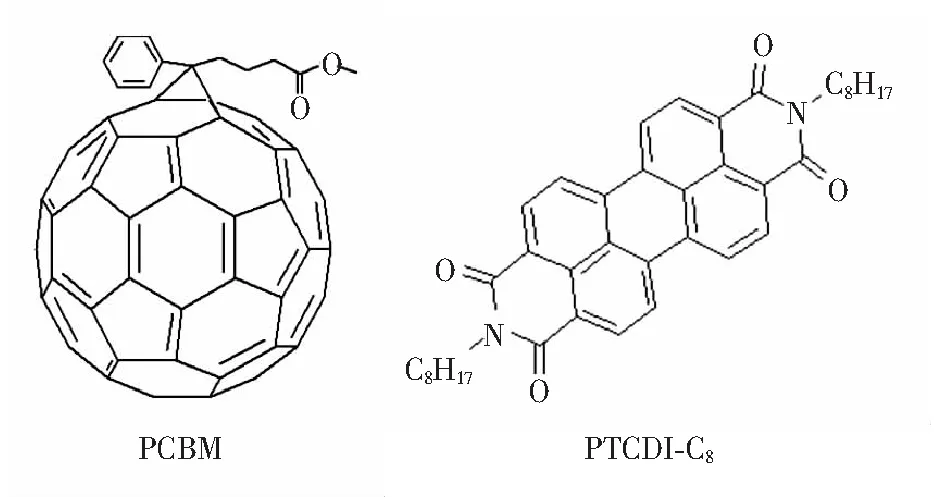
Fig.1 Molecular structure of PCBM and PTCDI-C8
2.2 Preparation of Perovskite Devices
The pre-cleaned ITO substrates were dried under an infrared lamp for 15 min, and then treated with UV/O3for 15 min. The PEDOT∶PSS layer of about 40 nm was fabricated by spin coating at 3 000 r/min for 30 s on ITO substrates, followed by baking at 120 ℃ for 25 min in the air. The PbI2solution (0.5 mol/L) was spin-coated on top of the PEDOT∶PSS film at 6 000 r/min for 30 s. Then the substrates were transferred to the glove box for the following device fabrication. The PbI2-coated films were annealed on a hotplate at 70 ℃ for 10 min. 120 μL of CH3NH3I isopropanol solution(0.24 mol/L) was spin-coated on top of the substrate at 6 000 r/min for 20 s. The perovskite films were treated at 60 ℃ for 10 min and then annealed at 100 ℃ for 20 min. 26 mg/mL PCBM DCB solution was then sequentially cast on top of the perovskite film by spin-coating at 6 000 r/min for 60 s and then dried on a 100 ℃ hot-plate for 10 min. Finally, PTCDI-C8film with thickness of 0-25 nm and 120 nm Al are thermally evaporated under vacuum at a pressure of 1×10⁻⁴Pa to form planar structure perovskite device. The effective area of the device is 0.1 cm2. Device architecture and energy level diagram are shown in Fig.2. The unpackaged devices are stored and periodically measured in the glove box.

Fig.2 Device structure(a) and schematic energy level diagram(b) of the planar heterojunction perovskite solar cells
3 Results and Discussion
J-Vcharacteristics of the perovskite solar cells with different thicknesses of PTCDI-C8layers are shown in Fig.3. Tab.1 lists the detailed device performance parameters (Jsc,Voc, FF and PCE). Optimal device performance is obtained at 20 nm PTCDI-C8thickness. Compared to the device without PTCDI-C8layer, PCE increased from 5.26% to 8.65%,Vocincreased from 0.86 V to 0.92 V,Jscincreased from 13.02 mA/cm2to 15.68 mA/cm2, and FF increased from 40.9% to 60%. That is to say, the PCE,Voc, FF andJscof the device are improved at the same time.
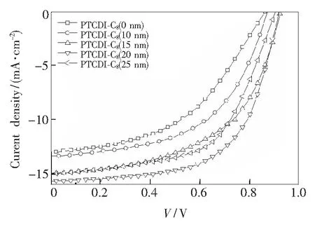
Fig.3J-Vcurves of the perovskite solar cells with different thickness of PTCDI-C8layers
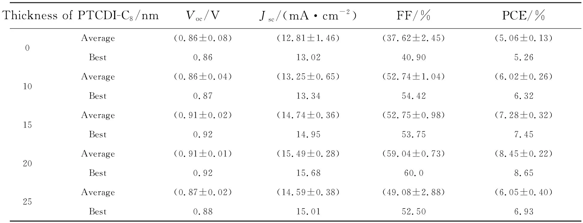
Tab.1 Summary of detailed performances for the PSCs with different thickness of PTCDI-C8 layers
Fig.4(a) shows the IPCE and integrated current density of the optimal device for PTCDI-C8with a thickness of 20 nm. The results indicate that the integral current is consistent with the current obtained from theJ-Vtest. TheJ-Vcurves(Fig.4(b)) obtained by forward scan is similar to that measured from reverse scan, which means that there is no obvious hysteresis. It reveals that the inserting of PTCDI-C8interfacial layer can significantly reduce hysteresis.
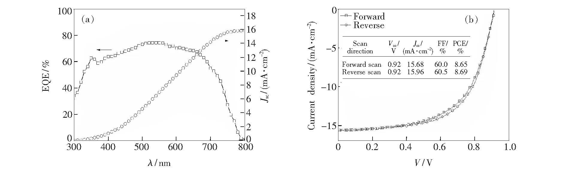
Fig.4 IPCE(a) and J-V(b)characteristic measured with the bias scanned in different direction for the optimal device

Fig.5 AFM and SEM images of CH3NH3PbI3(a, b), CH3NH3PbI3/PCBM (c, d) and CH3NH3PbI3/PCBM/PTCDI-C8(e, f) layers.
Fig.5 shows AFM and corresponding SEM images of CH3NH3PbI3, CH3NH3PbI3/PCBM and CH3NH3PbI3/ PCBM/PTCDI-C8films. The root mean square roughness (Rq) and average roughness (Ra) are 13.1 nm and 10.1 nm, respectively (Fig.5(a)). Fig.5(c) shows that theRq(10.0 nm) andRa(7.01 nm) roughness of PCBM sample are significantly lowered than that of perovskite films. For CH3NH3PbI3/PCBM/PTCDI-C8film,RqandRavalues are further reduced to 2.81 nm and 2.23 nm, respectively (Fig.5(e)). SEM imaging is consistent with the morphology of the AFM. Observed from the perovskite SEM images, it can be seen that PTCDI-C8deposited on the PCBM surface can form a more smooth and dense film. The introducing of PTCDI-C8layer can reduce the leakage current at the interface. Thereby, theJscandVocof the device are improved for the increasing of device charge collection efficiency.
Surface photovoltage spectroscopy (SPS) is used to determine the intensity of the response of the surface to light. Surface photovoltage is generated by the separation of photo-generated electron and hole in the device. Figure 6 shows SPS spectra of the samples with different thickness of PTCDI-C8layers. After PTCDI-C8deposited on the surface of the PCBM, the SPV response of the sample is obviously enhanced and reaches the maxmum value at the thickness of 20 nm. This means the exciton recombination is effectively inhibited. That is because of the low HOMO energy level of PTCDI-C8, which can block the movement of holes transmitting to the cathode, and improve the separation efficiency of photo-generated electrons and holes.
Fig.7 shows UV-Vis absorption spectra of PTCDI-C8(20 nm),CH3NH3PbI3/PCBM(40 nm) and CH3NH3PbI3/ PCBM/PTCDI-C8(20 nm) films. It shows that PTCDI-C8has obvious absorption in the range of 400-600 nm, which is a little help but not the key factors to improve the device performance. Fig.8 shows the relationship between normalized efficiency and storage time of perovskite cells with different thickness of PTCDI-C8. The device without PTCDI-C8buffer layer degrades significantly faster than that of with PTCDI-C8as cathode interfacial layer. The stability of the device is greatly improved. This means that the introduction of PTCDI-C8as cathode buffer layer improves the performance and stability of the device.

Fig.6 SPS measurements of the samples with different thickness of PTCDI-C8layers
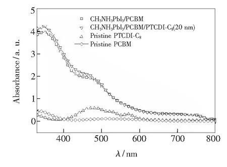
Fig.7 UV-Vis absorption spectra of PTCDI-C8, PCBM and CH3NH3PbI3/PCBM/PTCDI-C8(20 nm) film.
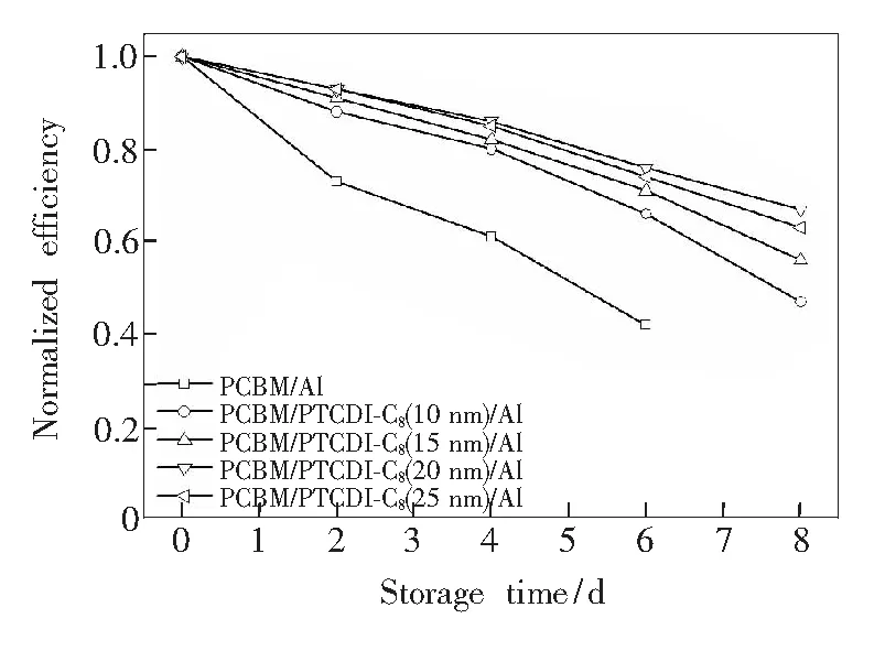
Fig.8 Relationship between normalized efficiency and storage time of perovskite cells with different thickness of PTCDI-C8layer
4 Conclusion
In this paper, PTCDI-C8film was used as the interfacial layer of the electron transport layer PCBM to reduce the leakage current between PCBM and Al electrode and to improve the electron collecting efficiency of cathode. By adjusting the thickness of PTCDI-C8film, the interfacial contact and electron transport properties were optimized. Compared with the control devices, the PCE of the optimal device achieves 8.65% with 20 nm thickness PTCDI-C8film, withVocof 0.92 V,Jscof 15.68 mA/cm2and a FF of 60%. PTCDI-C8layer can effectively block the hole transmitting to the cathode. With a higher electron mobility and stability, PTCDI-C8layer can also reduce the environment erosion on the PCBM. In summary, PTCDI-C8can be used as an effective cathode buffer layer in PSCs to improve device performance and stability.
