Electrodeposition and characterization of Cu2O thin films using sodium thiosulfate as an additive for photovoltaic solar cells☆
Hassiba Rahal,Ra fiaa Kihal,Abed Mohamed Affoune *,Samia Rahal
1 Laboratoire d'Analyses Industrielles et Génie des Matériaux,Département de Génie des Procédés,Faculté des Sciences et de la Technologie,Université 8 Mai 1945 Guelma,BP 401,Guelma 24000,Algeria
2 Université 20 Août 1955 Skikda,BP 26,Route El-Hadaiek,21000,Algeria
3 Université Abbes Laghrour Khenchela,BP 1252,Rue de Batna,Khenchela 40004,Algeria
4 Laboratoire d'Etude des Surfaces et Interfaces de la Matière Solide LESIMS,Département de Physique,Faculté des Sciences,Badji Mokhtar Université,Annaba,Algeria
1.Introduction
The total demand of energy in the world increases with the demographic growth and the development of technology.Among all renewable energy sources,solar energy is extremely useful and promising as an abundant and clean energy source[1].Photovoltaic conversion is one of the most advanced technologies,which consists in directly transforming solar energy into electric energy using semiconductor knowing that it has attracted attention for many decades.The high production cost of solar energy materials constitutes a serious drawback for the commercialization of photovoltaic cells.Furthermore,toxic substances are involved in the production and processing of most semiconductors,causing environmental problems.Thus,research efforts have been made especially in the last decade in order to develop materials which were able to guarantee optimal characteristics in terms of environmental compatibility,abundance and photoactivity[2].Among the various metal oxide materials,cuprous oxide(Cu2O)is regarded as a promising material because of its suitable band gap and high absorption coefficient in the visible-light region.In addition with good optical and electrical properties the material has many advantages such as availability and abundance of the starting materials,non-toxic nature and low production cost[3].Thus it is promising in various applications,including such as gas sensing[4],solar cell application[5],photocatalysis[6],thin film homo-junction solar cells[7],and photoelectrodes for solar water splitting[8,9]and was used as a working electrode in the application of photoelectrochemical solar cell(PESC)[10].
Various synthesis methods are usually used to prepare Cu2O thin films,such as sol gel[10],pulsed laser deposition[11],chemical vapor deposition[12],chemical bath deposition[13-15],solvothermal synthesis[16],silar deposition[5,17-19],electron beam evaporation[3]and electrodeposition[4,7-9,20-37].Besides these methods,electrode position provides several advantages over the other methods because of its simplicity,low equipment cost,the possibility of preparing large area of thin films and the control of the film thickness[33].Cu2O films are usually electrodeposited from copper precursor solution,such as copper nitrate[31,9],copper sulfate[8,23-27,30,32,35,37]and copper acetate[4,7,21,22,25,27-29,33-36].In order to improve the quality of the deposited films such as uniformity,adhesion and crystallinity,it is necessary to add a complexing agent into the electrolytic bath.Many researchers use various complexing agents such as polyvinyl pyrrolidone[16],lactic acid[8,20,23,27,38],tartaric acid[38],ethylene diamine tetra acetic acid[20],citric acid[20,26,37],oxalic acid[38],and malic acid[38,39],trisodium citrate[3,13],sodium lactate[30],triethanolamine[3]and sodium thiosulfate[14,15].Furthermore,sodium thiosulfate shows a promising complexing agent of the deposited Cu2O because of its non-toxicity and low-cost compared to other complexing agents[3,8,13-16,20,23,26,27,30,38,39].No work has been published concerning the electrodeposition of Cu2O using sodium thiosulfate as an additive with copper acetate as precursor.
The aim of this work is devoted to the preparation of Cu2O thin films onto ITO-coated glass substrates by electrodeposition technique in a solution containing copper acetate with sodium thiosulfate.Cyclic voltammetry and chronoamperometry were utilized to study the electrochemical behavior of electrolyte bath containing copper acetate.The effect of sodium thiosulfate on the electrochemical deposition,structure and morphology of Cu2O was investigated.Deposited films were characterized by X-ray diffraction(XRD),Fourier transform infrared spectroscopy(FTIR),scanning electron microscopy(SEM),optical,photoelectrochemical(PEC)and electrical measurements.
2.Experimental Details
2.1.Reagents
All chemical reagents used in the present work were of analytical grade.Copper acetate monohydrate(Cu(C2H3O2)2·H2O,98%,Sigma Aldrich)was used as copper sources.Sodium acetate trihydrate(CH3COONa·3H2O,99%,Sigma Aldrich)and sodium sulfate(Na2SO4,99%,Sigma Aldrich)were used as a supporting electrolyte.However,sodium thiosulfate pentahydrate(Na2S2O3·5H2O,99.5%,Sigma Aldrich)was used as complexing agent.All aqueous solutions were prepared with distilled water.
2.2.Preparation and characterization techniques of Cu2O thin films
Electrodeposition of Cu2O thin films was carried out using a three electrode electrochemical cell with a platinum(Pt)wire as a counter electrode,indium tin oxide(ITO)-coated glass(8-10 Ω·square-1,Sigma Aldrich)substrate was used as working electrode.A saturated calomel electrode(SCE)was used in all experiments as a reference electrode.Before the deposition,the substrates were cleaned ultrasonically in acetone and ethanol and then rinsed in distilled water for 7 min[37,40].Cuprous oxide films were electrodeposited in an aqueous solution of 0.01 mol·L-1Cu(C2H3O2)2·H2O,0.1 mol·L-1CH3COONa·3H2O and 1.2 mmol·L-1Na2S2O3·5H2O at 60 °C.The pH of solutions was adjusted to 6.2 by CH3COOH additions.Sodium thiosulfate is used to stabilize Cu2+ions in the solution[17-19].
Cyclic voltammetry and chronoamperometry studies were carried out using Princeton Applied Research Model 273 A Potentiostat/Galvanostat,coupled to a personal computer with Power Suite software for data acquisition and potential control.Cuprous oxide films were electrodeposited at-0.58 V for 30 min.Following the deposition,electrodeposited Cu2O films were dried in air at 100°C.
The crystalline phase of Cu2O films was investigated by X-ray diffraction using a Bruker Discover D8 Diffractometer with CuKαradiation(λ=0.15406 nm).FTIRspectra were recorded on a Shimadzu FTIR-8000 series spectrophotometer.Scanning electron microscopy imaging was performed using a VEGA3 TESCAN scanning electron microscope operating at 20 kV accelerating voltage.Optical transmittance of thin films was measured by a Perkin Elmer Lambda 950 UV-vis-NIR spectrometer.Photoelectrochemical measurements were carried out by cyclic voltammetry technique in a three electrode electrochemical cell using deposited Cu2O films as a working electrode,platinum wire as a counterelectrode and a saturated calomelelectrode(SCE)as a reference electrode from an aqueous solution containing 0.1 mol·L-1sodiumsulfate(Na2SO4).Atungsten halogen lamp(100 W)was used to illuminate an active area of 1 cm2of Cu2O electrode.Electrical properties of deposited Cu2O films were determined by a HMS 3000 Hall measurement system at room temperature.Ag-paste was used at the corners of films to make four good contacts with probes.Thickness of the films was measured using a Dektak stylus profilometer.
3.Results and Discussion
3.1.Electrochemical studies
3.1.1.Cyclic voltammetry
We made a comparison of cyclic voltammograms obtained onto ITO substrate of the solution containing 0.01 mol·L-1copper acetate and 0.1 mol·L-1sodium acetate without(Fig.1(a))and with 1.2 mmol·L-1sodium thiosulfate(Fig.1(b)).The potential sweep was ranged from 0.3 to-1.7 V with a scan rate of 50 mV·s-1.From Fig.1(a),we recorded two cathodic peaks.

Fig.1.Cyclic voltammograms of the solution containing 0.01 mol·L-1copper acetate and 0.1 mol·L-1 sodium acetate at pH=6.2 and T=60 °C,without(a)and with 1.2 mmol·L-1 sodium thiosulfate(b).
The firstcathodic peak at-0.56 V,which attributed to the reduction of Cu2+to Cu+where water converted to hydroxide ions molecule.The hydroxide ions react with Cu+in the solution to form Cu2O on the substrate according to the following reaction[26,27,41,42]:

The second cathodic peak is observed at-1.33 V which can be mainly ascribed to the deposition of metallic copper with release of Hydrogen(Eqs.(3)and(4)).

Similar cathodic peaks are reported in the literature[26,27,33,34,36,41-44],but the present cathodic peaks are shifted compared with literature.
During reverse scan,an anodic peak is observed at 0.29 V corresponding to the oxidation of metallic copper[26,41],indicating the only formation of Cu2O on the ITO substrate which is confirmed below by XRD analysis.From Fig.1(b),we can observe that in the presence of sodium thiosulfate,the cathodic peak currents of the formation of Cu2O and Cu are much higher which indicates an increase in the deposition rate of Cu2O and Cu thin films,whereas the oxidation peak current of metallic copper is increased compared to that without sodium thiosulfate(Table 1).This difference can be attributed to a complexation effect of the Cu2+ions by the sodium thiosulfate[14,15,17-19],leading to acceleration of the electrochemical reaction kinetics for the formation of Cu2O films.The cathodic peak current of the formation of Cu2O with sodium thiosulfate is about-5.4 mA.This value is higher than that of other additives[23,26,32,36].
To study the effect of the scan rate on the reduction of copper Cu(II)ions,we performed a study by cyclic voltammograms at different scan rates ranging from 30 to 100 mV·s-1which are shown in Fig.2.From this figure,it was noted that the current of anodic and cathodic peaks increases with the increase of scan rates and the cathodic peak potentials have shifted towards negative values.This indicates the presence of a chemically irreversible electrochemical reaction.
Also,the cathodic peak current for the formation of Cu2O(Ipc)varied linearly with the square root of scan rate(Fig.3),suggesting that the electrochemical reaction is diffusion controlled.According to Bard and Faulkner[45],the following equation(Eq.(5))gives the relationship between the peak potential,the half peak potential and the electrontransfer coefficient for an irreversible electrochemical reaction:

where Epcis the cathodic peak potential(V),Epc/2is the half cathodic peak potential(V),α′is the electron-transfer coefficient,R is the gas constant(J·mol-1·K-1),T is the absolute temperature(K)and F is the Faraday constant(C·mol-1).From Fig.2,we can obtain the half cathodic peak potential(Epc/2),the cathodic peak potential(Epc),and │Epc-Epc/2│ =0.24 V.α′can be calculated from Eq.(5)which is estimated to be 0.22.
The diffusion coefficient can be calculated using the Randles-Sevcik relation(Eq.(6))[46]:

where Ipcis the cathodic peak current(A),n is the number of electrons exchanged during the redox process,A′(cm2)is the active area of the working electrode,C is the bulk concentration of the electroactive species(mol·cm-3)(the concentration of the species),D′is the diffusion coefficient(cm2·s-1)and V is the voltage scan rate(V·s-1).The diffusion coefficient was calculated to be 3.61×10⁻⁴cm2·s-1at 333 K.
3.1.2.Chronoamperometry

Fig.2.Cyclic voltammograms of the solution containing 0.01 mol·L-1 copper acetate and 0.1 mol·L-1 sodium acetate at pH=6.2 and T=60 °C with 1.2 mM sodium thiosulfate at various scan rates.

Fig.3.Plot of I pc versus V1/2 for the formation of Cu2O from cyclic voltammograms of Fig.2.
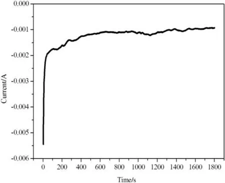
Fig.4 shows the chronoamperometry curve for the deposition of Cu2O films onto ITO substrate with sodium thiosulfate at T=60°C and E=-0.58 V.The current starts with high value,which is assigned to a rapid nucleation growth.The decrease of cathodic current with the increase of time is due to the depletion of the metal-ion concentrations close to the electrode surface.The current stabilized ateven longer time(1800 s).This confirms that the limited value of the stationary current is related to the formation of cuprous oxide on the surface.A similar behavior was observed for different copper salt solutions with other complexing agents[26].
3.2.Characterization of Cu2O thin films
3.2.1.XRD analysis
The thickness of the deposited films was measured to be 250 nm.Fig.5 shows the XRD patterns of Cu2O films deposited onto ITOsubstrates without(Fig.5(a))and with sodium thiosulfate(Fig.5(b)).From this figure,all the diffraction peaks of Cu2O thin films correspond to the peaks of cubic phase of standard Cu2O(JCPDS 05-0667)[34].X-ray diffraction patterns show that the intensity of the(200)diffraction peak is higher when compared with the other peaks,indicating preferential orientation along the c-axis.It is seen that the film deposited with sodium thiosulfate shows a new(111)diffraction peak of Cu2O phase and the intensity of the diffraction peaks is significantly higher than that of the films prepared without sodium thiosulfate.It indicates that the good crystallinity of deposited Cu2O films is improved with the addition of sodium thiosulfate.

Table 1 Electrochemical parameters obtained from cyclic voltammograms

Fig.4.Chronoamperometry curve for the deposition of Cu2O films.

Fig.5.X-ray diffraction of Cu2O films deposited onto ITO substrates,without(a)and with sodium thiosulfate(b).
The calculated value of the lattice constant parameter for the Cu2O films(a=b=c=0.425 nm)was slightly different than that of standard Cu2O(JCPDS 05-0667,a=b=c=0.4269 nm)[47,49].

The crystallite size(D)of Cu2O thin films was calculated from the major diffraction peaks of the base of(200)using Scherrer's formula(Eq.(7))[5,13,26]:where λ is the wavelength of the incident beam(0.15406 nm),β is the full width at half maximum and θ is Bragg's angle in rad.The average crystallite size of deposited Cu2O with sodium thiosulfate is found to be 23.22 nm.This value is greater than that of Cu2O films without sodium thiosulfate(22.45 nm).
The comparison of the observed d values of Cu2O films with JCPDS data(05-0667)is shown in Table 2.The value of d-spacing for Cu2O films obtained was slightly different than that of the d-spacing for standard Cu2O[JCPDS 05-0667],suggesting that all the Cu2O films exhibited a tensile strain and dislocation density,which is reported by others[5,11].

Table 2 Comparison of the observed d values of Cu2O films with JCPDS data(05-0667)
The dislocation density(δ),defined as the length of dislocation lines per unit volume,was evaluated from the formula(Eq.(8))[5]:

Strain(ε)of the films was calculated by the formula(Eq.(9))[5]:

The evaluated structural parameters of deposited Cu2O with sodium thiosulfate are regrouped in Table 3,which represents the values of full width at half maximum,the crystallite size,the dislocation density(δ)and the strain(ε)of the Cu2O thin films from the(200)direction.

Table 3 Structural parameters of Cu2O thin films
3.2.2.FT–IR analysis
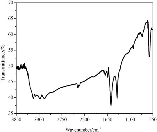
The Cu2O films deposited with sodium thiosulfate were also examined by FTIR spectroscopy which spectrum is shown in Fig.6.From this spectrum,the absorption band at 634 cm-1is attributed to the stretching vibration of Cu--O in Cu2O[47,48].The observed absorption bands at 1414.18 cm-1and 1566.27 cm-1are due to the presence of the carboxylate group(COO-)and correspond to the symmetric stretching and asymmetric stretching vibrations of the C--O band in the acetate group,respectively[47-50].We also note the presence of bands at 3168.265 to 3442.608 cm-1assigned to the stretching vibration of--OH groups of adsorbed water molecules[48,50,51].
3.2.3.SEM analysis
The surface morphologies of Cu2O films deposited onto ITO substrates obtained without and with sodium thiosulfate are shown in Fig.7(a)and(b)respectively.The surface morphologies of deposited Cu2O films prepared without sodium thiosulfate(Fig.7(a))are covered with a single type of small grains.The grains are well defined,spherical shape and an almost similar size(400 nm).In the presence of sodium thiosul fate(Fig.7(b)),morphology doesnot change but there is a better compactness with increasing size(650 nm)of the spherical grains.Such type of spherical shape is also observed when Cu2O thin films deposited onto various substrates by different copper salt solutions[14,32].

Fig.6.FTIR spectrum of Cu2O films.
3.2.4.Optical properties
The optical transmittance spectrum of Cu2O films deposited onto ITO substrates with sodium thiosulfate from a wavelength range of 400-1100 nm taken at room temperature is shown in Fig.8.It was shown that the films present a high optical transmission(>80%)in the visible wavelength range,which confirms the good optical quality of the electrodeposited Cu2O thin films.The absorption coefficient(α)was determined in the order of>104cm-1.
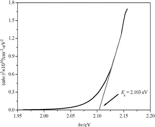
The plot of(αhν)2versus photon energy(hν)of deposited films was presented in Fig.9.It has been observed that the plots of(αhν)2versus(hν)are linear over a wide range of photon energies indicating the direct type of transitions.The band gap of the films was determined from Tauc's formula which is as follows(Eq.(10))[22,27,42]:


Fig.8.Transmittance spectrum of Cu2O films.

Fig.9.Plot of(αhν)2 versus hν of Cu2O films.

Fig.7.SEM images of Cu2O films deposited onto ITO substrates,without sodium thiosulfate(a)and with sodium thiosulfate(b).
whereαis the absorption coefficient,h is Planck's constant,νis the photon energy,A is a constant and Egis the direct transition band gap.The optical band gap value was determined by extrapolating the linear portion of the plot of(αhν)2versus photon energy(hν),which is illustrated in Fig.9.The band gap of Cu2O thin films was estimated to be 2.103 eV,which is in good agreement with the values reported for Cu2O films by others[28,34].The obtained energy gap results make Cu2O film as a promising semiconductor material for fabrication of photovoltaic solar cells.
3.2.5.Photoelectrochemical measurements
Fig.10 shows the photoelectrochemical(PEC)response of cuprous oxide(Cu2O)deposited onto ITO substrates with sodium thiosulfate at-0.58 V for the solution containing 0.1 mol·L-1sodium sulfate(Na2SO4),in the dark(a)and under illumination(b).In the dark,there is a negligible anodic photocurrent.However,under illumination of the surface of deposited cuprous oxide,we observe an important anodic photocurrentcompared with in the dark indicating the carriers are generated at the Cu2O film electrode under irradiation[21,52,53].These observations suggested that the photogenerated charge carrier holes(h+)can promote oxidation reaction at the semiconductor/electrolyte solution interface.The anodic photocurrent generation represents the typical behavior of the n-type semiconductor of the Cu2O thin films[21,25,29].This n-type semiconductor was observed when Cu2O thin films electrodeposited onto various substrates[4,27-29,33,34,36].

Fig.10.Photoelectrochemical response of Cu2O films,in the dark(a)and under illumination(b).
3.2.6.Electrical properties
The Hall Effect measurement results showed that the Cu2O films deposited with sodium thiosulfate have n-type conductivity with a carrier concentration of-4.94 × 1015cm-3,mobility of 20.61 cm2·V-1s-1and low electrical resistivity of 61.30 Ω·cm-1.These values are in agreement with the results reported by others[24,35].
4.Conclusions
Cuprous oxide(Cu2O)thin films have been successfully electrodeposited onto ITO-coated glass substrates from aqueous copper acetate solutions with addition of sodium thiosulfate at 60°C.We found that the addition of sodium thiosulfate has a strong effect on the electrochemical reaction kinetics,crystallinity and morphology of Cu2O thin films.Cu2O thin films were deposited at-0.58 V for 30 min with a film thickness of about 250 nm.X-ray diffraction analysis revealed that the synthesized Cu2O thin films have a cubic phase.The crystallite size was estimated to be 23.22 nm.FTIR results confirmed the presence of Cu2O films at peak 634 cm-1.SEM images of Cu2O films showed a better compactness and consist of spherical shape.Photoelectrochemical measurements of Cu2O thin films showed that this film behaves as a semiconductor of n-type and presents high photo anodic-generated currents.These films exhibited a high optical transmission(>80%)and high absorption coefficient(α > 104cm-1)in the visible-light region.The optical energy band gap was found to be 2.103 eV.Hall Effect measurement results confirmed that the Cu2O thin films have n-type conductivity with a low electrical resistivity of 61.30 Ω·cm-1,carrier concentration of-4.94×1015cm-3and mobility of 20.61 cm2·V-1s-1.Taken into account of its non-toxicity and lowcost,sodium thiosulfate could be used as a promising complexing agent to prepare Cu2O thin films with suitable properties for fabrication of photovoltaic solar cells.
[1]B.S.Pawar,S.M.Pawar,S.W.Shin,D.S.Choi,C.J.Park,S.S.Kolekar,J.H.Kim,Effect of complexing agent on the properties of electrochemically deposited Cu2ZnSnS4(CZTS)thin films,Appl.Surf.Sci.257(2010)1786-1791.
[2]A.S.Arico,D.Silvestro,P.L.Antonucci,N.Giordano,V.Antonucci,Electrode posited thin film ZnTe semiconductors for photovoltaic applications,Adv.Perform.Mater.4(1997)115-125.
[3]R.Oommen,U.Rajalakshmi,Sanjeeviraja,Characteristics of electron beam evaporated and electrodeposited Cu2O thin films—comparative study,Int.J.Electrochem.Sci.7(2012)8288-8298.
[4]P.A.Praveen Janantha,L.N.L.Perera,K.M.D.C.Jayathilaka,J.K.D.S.Jayanetti,D.P.Dissanayaka,W.P.Siripala,Use of Cu2O microcrystalline thin film semiconductors for gas sensing,Proc.Tech.Sess.Inst.Phys-Sri Lanka,25,2009,pp.70-76.
[5]N.Soundaram,R.Chandramohan,S.Valanarasu,R.Thomas,A.Kathalingam,Studies on SILAR deposited Cu2O and ZnO films for solar cell application,J.Mater.Sci.Mater.Electron.26(7)(2015)5030-5036.
[6]J.Dong,H.Xu,F.Zhang,Ch.Chen,L.Liu,G.T.Wu,Synergistic effect over photocatalytic active Cu2O thin films and their morphological and orientational transformation under visible light irradiation,Appl.Catal.,A 470(2014)294-302.
[7]R.P.Wijesundera,L.K.A.D.D.S.Gunawardhana,W.Siripala,Electrodeposited Cu2O homojunction solar cells:fabrication of a cell of high short circuit photocurrent,Sol.Energy Mater.Sol.Cells 157(2016)881-886.
[8]Q.Ma,J.P.Hofmann,A.Litke,E.J.M.Hensen,Cu2O photoelectrodes for solar water splitting:tuning photoelectrochemical performance by controlled faceting,Sol.Energy Mater.Sol.Cells 141(2015)178-186.
[9]Zh.Zhang,P.Wang,Highly stable copper oxide composite as an effective photocathode for water splitting via a facile electrochemical synthesis strategy,J.Mater.Chem.22(2012)2456-2464.
[10]D.S.C.Halin,I.A.Talib,A.R.Daud,M.A.A.Hamid,Characterizations of cuprous oxide thin films prepared by sol-gel spin coating technique with different additives for the photoelectrochemical solar cell,Int.J.Photoenergy 2014(352156)(2014)1-6.
[11]G.Kaur,A.Mitra,K.L.Yadav,In fluence of oxygen pressure on the growth and physical properties of pulsed laser deposited Cu2O thin films,J.Mater.Sci.Mater.Electron.26(2015)9689-9699.
[12]M.M.Kareem,A.H.A.Al-Fouadi,D.H.Hussain,Preparation and study of Cu2O thin film at low temperature by Chemical vapor deposition(CVD)route,Int.J.Appl.Innov.Eng.Manag.4(12)(2015)63-66.
[13]H.Xu,J.Dong,Ch.Chen,One-step chemical bath deposition and photocatalytic activity of Cu2O thin films with orientation and size controlled by a chelating agent,Mater.Chem.Phys.143(2014)713-719.
[14]P.B.Ahirrao,S.R.Gosavi,D.R.Patil,M.S.Shinde,R.S.Patil,Photoluminescence properties of modi fied chemical bath deposited copper oxide thin film,Arch.Appl.Sci.Res.3(2)(2011)288-291.
[15]M.R.Johan,M.Sh.M.Suan,N.L.Hawari,H.A.Ching,Annealing effects on the properties of copper oxide thin films prepared by chemical deposition,Int.J.Electrochem.Sci.6(2011)6094-6104.
[16]M.A.Khan,M.Ullah,T.Iqbal,H.Mahmood,A.A.Khan,M.Sha fique,A.Majid,A.Ahmed,N.A.Khan,Surfactant assisted synthesis of cuprous oxide(Cu2O)nanoparticles via solvothermal process,Nanosci.Nanotechnol.Res.3(1)(2015)16-22.
[17]S.S.Nikam,M.P.Suryawanshi,S.M.Bhosale,M.A.Gaikwad,P.A.Shinde,A.V.Moholkar,Cu2O thin films prepared using modi fied successive ionic layer adsorption and reaction method and their use in photoelectrochemical solar cells,J.Mater.Sci.Mater.Electron.27(2)(2016)1897-1900.
[18]S.S.Oluyamo,Nyagba,S.Mbafan,Ojo,S.Ambrose,Optical properties of copper(I)oxide thin films synthesized by SILAR technique,J.Appl.Phys.6(3)(2014)102-105.
[19]A.T.Ravichandran,K.Dhanabalan,R.Chandramohan,A.Vasuhi,P.Parameswaran,Optical properties of modi fied-silar grown copper oxide nanocrystalline thin films,Int.J.Inf.Res.Rev.1(1)(2014)007-011.
[20]Zh.Zhang,W.Hu,Y.Deng,Ch.Zhong,H.Wang,Y.Wu,L.Liu,The effect of complexing agents on the oriented growth of electrodeposited microcrystalline cuprous oxidefilm,Mater.Res.Bull.47(2012)2561-2565.
[21]Y.Yang,J.Han,X.Ning,W.Cao,W.Xu,L.Guo,Controllable morphology and conductivity of electrodeposited Cu2O thin film:effect of surfactants,Appl.Mater.Interfaces 6(24)(2014)22534-22543.
[22]X.Jiang,M.Zhang,Sh.Shi,G.He,X.Song,Zh.Sun,Microstructure and optical properties of nanocrystalline Cu2O thin films prepared by electrodeposition,Nanoscale Res.Lett.9(2014)219-223.
[23]J.Morales,L.Sanchez,S.Bijani,L.Martinez,M.Gabas,J.R.Ramos-Barrado,Electrodeposition of Cu2O:an excellent method for obtaining films of controlled morphology and good performance in Li-ion batteries,Electrochem.Solid-State Lett.8(3)(2005)A159-A162.
[24]Y.Abdu,A.O.Musa,T.H.Darma,Electroless deposition and electrical characterization of n-Cu2O layer,Baye.J.Pure Appl.Sci.5(2)(2012)1-10.
[25]P.Wang,H.Wu,Y.Tang,R.Amal,Y.H.Ng,Electrodeposited Cu2O as photoelectrodes with controllable conductivity type for solar energy conversion,J.Phys.Chem.C 119(2015)26275-26282.
[26]S.Laidoudi,A.Y.Bioud,A.Azizi,G.Schmerber,J.Bartringer,S.Barre,A.Dinia,Growth and characterization of electrodeposited Cu2O thin films,Semicond.Sci.Technol.28(11)(2013)115005-115011.
[27]A.El-Shaer,M.T.Y.Tadros,M.A.Khalifa,Fabrication of homojunction cuprous oxide solar cell by electrodeposition method,Nat.Sci.13(5)(2015)1-9.
[28]A.El-Shaer,A.R.Abdelwahed,M.M.Mosaad,A.Taw fik,D.Hemada,Effect of pH on conductivity of electrodeposited cuprous oxide thin films,Nat.Sci.13(3)(2015)1-5.
[29]K.D.R.N.Kalubowila,L.K.A.D.D.S.Gunawardhana,R.P.Wijesundera,W.Siripala,Methods for improving n-type photoconductivity of electrodeposited Cu2O thin films,Semicond.Sci.Technol.29(7)(2014)075012-075018.
[30]X.Han,K.Han,M.Tao,Characterization of Cl-doped n-type Cu2O prepared by electrodeposition,Thin Solid Films 518(2010)5363-5367.
[31]H.Li,R.Liu,R.Zhao,Y.Zheng,W.Chen,Zh.Xu,Morphology control of electrodeposited Cu2O crystals in aqueous solutions using room temperature hydrophilic ionic liquids,Cryst.Growth Des.6(12)(2006)2796-2798.
[32]Y.Yang,Y.Li,M.Pritzker,Control of Cu2O film morphology using potentiostatic pulsed electrodeposition,Electrochim.Acta 213(2016)225-235.
[33]R.P.Wijesundera,M.Hidaka,K.Koga,M.Sakai,W.Siripala,Growth and characterisation of potentiostatically electrodeposited Cu2O and Cu thin films,Thin Solid Films 500(2006)241-246.
[34]P.Grez,F.Herrera,G.Riveros,A.Ramirez,R.Henriquez,E.Dalchiele,R.Schrebler,Morphological,structural,and photoelectrochemical characterization of n-type Cu2O thin films obtained by electrodeposition,Phys.Status Solidi A 209(12)(2012)2470-2475.
[35]T.Jiang,T.Xie,W.Yang,L.Chen,H.Fan,D.Wang,Photoelectrochemical and photovoltaic properties of p-n Cu2O homojunction films and their photocatalytic performance,J.Phys.Chem.C 117(2013)4619-4624.
[36]A.S.M.Hanif,F.Mohamad,R.Z.Zakaria,Cyclic voltammetry measurement for n-type Cu2O thin film using copper acetate-based solution,J.Eng.Appl.Sci.10(19)(2015)8562-8568.
[37]D.Mohra,M.Benhaliliba,M.Serin,M.R.Khelladi,H.Lahmar,A.Azizi,The investigation of electrodeposited Cu2O/ITO layers by chronocoulometry process:effect of electrical potential,J.Semicond.37(10)(2016)1-7.
[38]T.Fujiwara,T.Nakaue,M.Yoshimura,Direct fabrication and patterning of Cu2O film by local electrodeposition method,Solid State Ionics 175(2004)541-544.
[39]Q.Zhu,Y.Zhang,J.Wang,F.Zhou,P.K.Chu,Microwave synthesis of cuprous oxide micro-/nanocrystals with different morphologies and photocatalytic activities,J.Mater.Sci.Technol.27(4)(2011)289-295.
[40]G.Li,C.Dawa,Q.Bu,F.Zhen,X.Lu,Zh.Ke,H.Hong,Ch.Yao,P.Liu,Y.Tong,Electrochemical synthesis of orientation-ordered ZnO nanorod bundles,Electrochem.Commun.9(2007)863-868.
[41]G.Riveros,A.Garmendia,D.Ramirez,M.Tejos,P.Grez,H.Gomez,E.A.Dalchiele,Study of the electrodeposition of Cu2O thin films from DMSO solution,J.Electrochem.Soc.160(1)(2013)D28-D33.
[42]A.El-Shaer,A.R.Abdelwahed,A.Taw fik,M.Mossad,D.Hemada,Effect of deposition parameters on electrodeposited cuprous oxide thin films,Int.J.Emerg.Technol.Adv.Eng.4(12)(2014)595-602.
[43]Y.Tang,Zh.Chen,Zh.Jia,L.Zhang,J.Li,Electrodeposition and characterization of nanocrystalline cuprous oxide thin films on TiO2films,Mater.Lett.59(2005)434-438.
[44]C.Bogatu,M.Voinea,A.Duţă,I.M.Pelin,G.Ch.Chiţanu,The electrochemical deposition of Cu/CuOxsolar selective coatings with controlled morphology,Rev.Roum.Chim.54(3)(2009)235-241.
[45]A.J.Bard,L.R.Faulkner,Electrochemical Methods:Fundamentals and Applications,John Wiley&Sons,New York,2001.
[46]G.Li,C.Dawa,Q.Bu,X.Lu,Zh.Ke,H.Hong,F.Zheng,Ch.Yao,G.Liu,Y.Tong,Electrochemical self-assembly of ZnO nanoporous structures,J.Phys.Chem.C 111(2007)1919-1923.
[47]Z.C.Orel,A.Anzlovar,G.Drazic,M.Zigon,Cuprous oxide nanowires prepared by an additive-free polyol process,Cryst.Growth Des.7(2)(2007)453-458.
[48]S.E.Bouzit,B.Boualy,L.El Firdoussi,A.Mehdi,A.Outzourhit,M.A.Ali,Fast room temperature solution-phase approach for selective synthesis of nanostructured Cu(OH)2,Cu2O and CuO,Int.Res.J.Pure Appl.Chem.8(3)(2015)157-164.
[49]M.A.Amrani,V.V.S.S.Srikanth,N.K.Labhsetwar,A.S.Al-Fatesh,H.Shaikh,Phoenix dactylifera mediated green synthesis of Cu2O particles for arsenite uptake from water,Sci.Technol.Adv.Mater.17(1)(2016)760-768.
[50]E.Gražėnaitė,J.Kiuberis,A.Beganskienė,J.Senvaitienė,A.Kareiva,XRD and FTIR characterisation of historical green pigments and their lead-based glazes,CHEMIJA 25(4)(2014)199-205.
[51]M.M.Momeni,Z.Nazari,A.Kazempour,M.Hakimiyan,S.M.Mirhoseini,Preparation of CuO nanostructures coating on copper as supercapacitor materials,Surf.Eng.30(11)(2014)775-778.
[52]L.Xiong,T.Wai Ng,Y.Yu,D.Xia,H.Y.Yip,G.Li,T.An,H.Zhao,P.K.Wong,N-type Cu2O film for photocatalytic and photoelectrocatalytic processes:its stability and inactivation of E.coli,Electrochim.Acta 153(2015)583-593.
[53]J.L.Ropero-Vega,A.M.Meléndez,J.A.Pedraza-Avella,R.J.Candal,M.E.Niño-Gómez,Mixed oxide semiconductors based on bismuth for photoelectrochemical applications,J.Solid State Electrochem.18(2014)1963-1971.
 Chinese Journal of Chemical Engineering2018年2期
- Chinese Journal of Chemical Engineering的其它文章
- Surface chemical characterization of deactivated low-level mercury catalysts for acetylene hydrochlorination☆
- Insight into fouling behavior of poly(vinylidene fluoride)(PVDF)hollow fiber membranes caused by dextran with different pore
- Protein adsorption onto diethylaminoethyl dextran modi fied anion exchanger:Effect of ionic strength and column behavior☆
- Gas emission source term estimation with 1-step nonlinear partial swarm optimization-Tikhonov regularization hybrid method☆
- Dissolution of antibiotics mycelium in ionic liquids:Performance and mechanism☆
- Kinetic studies on extra heavy crude oilupgrading using nanocatalysts by applying CFD techniques☆
