电致发光用于大功率半导体激光器失效模式分析
2018-02-28 09:23:29刘启坤孔金霞朱凌妮刘素平马骁宇
发光学报 2018年2期
刘启坤, 孔金霞, 朱凌妮, 熊 聪, 刘素平, 马骁宇
(1. 中国科学院半导体研究所 光电子器件国家工程研究中心, 北京 100083; 2. 中国科学院大学 材料科学与光电技术学院, 北京 100049)
1 Introduction
High-power diode lasers have been studied for decades for their wide applications in industrial, communication, military, civil, medical,etc. For 975 nm high-power diode lasers, one of the most important applications is used as pumping sources for the erbium-doped fiber amplifiers (EDFAs) . Moreover, when a 975 nm high-power laser is coupled into a fiber, both the beam quality and output optical power can be promoted[1], which extends the applications. To further widen the applications of high-power laser diodes, higher power and more reliable devices are required.
A great effort is devoted to understanding the main causes to the failure of high-power laser diodes by many groups[2-7]. Generally speaking, the symptoms of the degradation include: (a) the decrease of the optical power (under the constant current); (b) the increase of the threshold current, operation voltage and divergence angle;(c) facet degradation; (d) wavelength shift;etc.
Because of the unperfect substrates, epitaxy layers, defects and strain that introduced by processing steps, together with external factors, such as current injection, optical power, and operation atmosphere, the degradation mechanism is rather complex. By facet passivation and coating, quantum well intermixing, non-injection regions in the vicinity of the facets, both the power and reliability have been promoted significantly. However, the mechanism of the degradation is not totally understood yet.
To achieve higher power and more reliable lasers, the catastrophic optical damage (COD) must be suppressed, for its suddenly occurrence without a previous sign[8]. Once the COD happens, the laser fails totally. When the COD is associated with the facets, it is called catastrophic optical mirror damage (COMD); when it happens in the bulk, it calls catastrophic optical bulk damage (COBD). The COD process usually associates with DLDs in the active region. By means of electron beam-induced current (EBIC)[8],optical beam-induced current (OBIC)[9], cathode luminescence (CL)[10-11]and electroluminescence (EL)[6], the DLDs appear, since the DLDs are damaged regions and full of non-radiative recombination centers.
In this paper, we performed EL on the suddenly failed 975 nm strained quantum well laser diodes. The EL images reveal regions with dark contrast corresponding to the DLDs that generated during the laser degradation process. We found that the COD not only happened at the facets (COMD), but also in the bulk (COBD), which is really valuable for our further refinement. And the common features of the DLDs of two typical COD modes were interpreted and compared. Furthermore, the causes to the two COD modes were analyzed. In addition, we made some suggestions to suppress the COD process and further refine the laser diodes.
2 Laser Structure and Experimental Setup
In this paper, the broad-area diode lasers lasing at 975 nm were grown on n-GaAs substrates by metalorganic chemical vapor deposition (MOCVD). As Fig.1 shows, the structure of the lasers is strained Single-quantum-well separate-confinement-heterostructure (SQW-SCH). The AlGaInAs QW was undoped with width of 8 nm. It was embedded in the undoped AlGaAs waveguide layers, and the thickness is 400 nm and 900 nm, respectively. And the cladding layers are 1 100 nm p-doped and 1 400 nm n-doped AlGaAs. The cavity length was 3.5 mm and the width of the active region is 80 μm. And near both facets, the injection current is blocked by the oxide mask, forming the non-injection regions. The front facets of the lasers were anti-reflection (AR) coated with reflectivity of 5%, and high-reflection (HR) coated with reflectivity of 95% for the rear facets. The isolator is SiO2. The p-contact is Ti/Pt/Au and the n-contact is Au/Ge/Ni. The total thickness of the laser chip is about 120 μm. The laser chip was mounted p-side down on submount by AuSn solder, which is so called COS (chip on submount) laser diode, as Fig.2 shows. The lasers operate in continuous wave operation and the typical optical output power of these lasers is 12 W atI=12 A and the temperature of the heat-sink (Ths) is 20 ℃.

Fig.1 Structure of the stained SQW-SCH laser diode chip

Fig.2 Schematic diagram of the COS laser diode
The aging tests were performed in continuous wave atI=12 A,Ths=20 ℃. After the lasers failed, the EL was employed to perform the failure mode analysis (FMA). Fig.3 shows the laser diode chip sample to perform EL. The n-contacts were removed by grinding and polishing. The EL images were taken under the condition ofI=200~300 mA (lower than the typical threshold current) at room-temperature. In addition, the lasers were not just from one wafer.
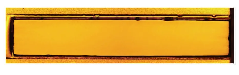
Fig.3 Laser diode chip sample to perform EL
3 Results and Discussion
In general, the failure modes can be classified as rapid, gradual and catastrophic degradation[7]. Fig.4 shows the typicalP-tcurves of three degradation modes under constant current. We can see that three degradation modes present the different features: for the rapid degradation mode, the optical power usually drops during the first hundred hours of operation; for the catastrophic degradation mode, the optical power drops suddenly and it can happen at any time during the operation; and for the gradual degradation mode, the optical power decreases gradually and the laser may last for several thousand hours.

Fig.4 TypicalP-tcurves of three degradation modes under constant current. (a) Rapid degradation mode. (b) Catastrophic degradation mode. (c) Gradual degradation mode.
A COD happens along with a thermal runaway process[2]. The heat generates from different aspects[12], and among them the non-radiative recombination plays a critical role. For example, the surface recombination and the presence of non-radiative recombination centers (NRRCs) in the bulk generate a large amount of heat and the temperature is increased locally, thus narrowing the locals bandgap which contributes to the enhanced self-absorption, so the temperature further increases, forming a feedback loop; finally, the large stress leads to the broken of the atom bonds and the lattice disorders, thus the COD occurs. When performing the EL on the failed lasers, the DLDs were shown, which are the result of melting and recrystallization. The DLDs are usually guided by the optical field and confined in the cavity. The COD process will be even worse to QW lasers for their reduced dimension of the QW thickness and the presence of interfaces[13-14].
Because of the asymmetric coating of the facets, the photon density, carrier density and temperature profiles in the cavity are inhomogeneous and may be asymmetric[15]. Together with the quality of the epitaxy layers and the facet coatings, the COD may happen at the facets and in the bulk.
In this paper, the EL images reveal that 90 lasers suffered COD among all the failed lasers. 62 lasers suffered COMD and 28 lasers suffered COBD.
3.1 COMD
Among all the 62 lasers suffered COMD, 37 lasers suffered COMD at the front facets and 25 lasers suffered COMD at the rear facets.
3.1.1 COMD at The Front Facet
We identified two typical DLDs patterns at the front facets: “one point” COMD and “multiple points” COMD. As Fig.5 shows, the EL images real the damaged area in the active regions and the optical images present the melted facets. And we can clearly see that the damaged area in the active regions and front facets are quite different, both in size and position.
Fig.5(a)-(c) show the “one point” COMD. The EL image Fig.5(a) shows that the DLDs originate from “one point” at the front facet and extend into the active region about 1/2 of the cavity. Under higher magnification (200×), we can see that the point expands in the vicinity of the front facet just as the EL image Fig.5(b) presents. The optical image (c) presents that the scale of the melting point is about 10 μm.
Fig.5(d)-(f) show the “multiple points” COMD. The EL image Fig.5(d) shows that the DLDs originate from “multiple points” of the front facet and extend into the active region. Under higher magnification (200×), we can clearly see that the multiple points originate from the front facet and expand into the active region in different orientations just as the EL image Fig.5(e) presents. The optical image Fig.5(f) presents the complete damage of the front facet. The “multiple points” correspond to the bolder points along the damage line.
All the images show that the DLDs originate from the front facet and extend into the active region in different orientations, and the DLDs are confined in the active region. The different surface recombination, distribution of the optical flux and carrier density may result in the different heat distributions at the facet, thus leading to the different melting points.
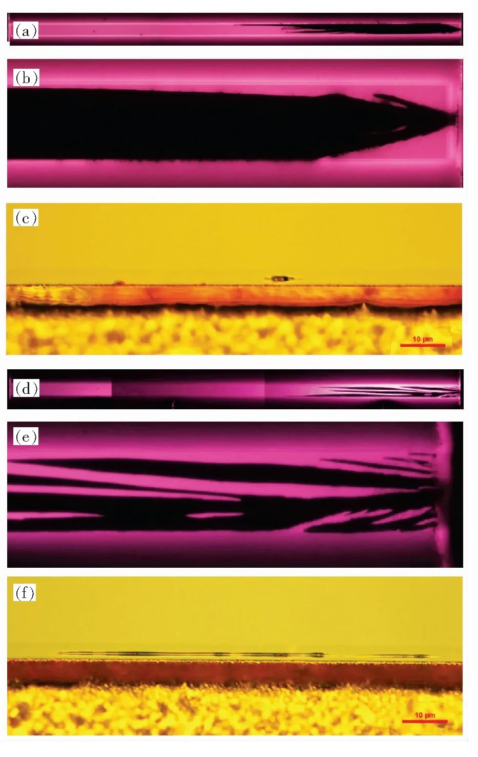
Fig.5 EL and optical images of the COMD at the front facets. (a) EL image of “one point” COMD at the front facet (50×). (b) EL image of the front part of the DLDs (200×). (c) Typical optical image of the facet with “one point” COMD (1 000×). (d) EL image of “multiple points” COMD at the front facet (50×). (e) EL image of the front part of the DLDs (200×). (f) Typical optical image of the facet with “multiple points” COMD (1 000×).
In addition, among all the 37 lasers suffered COMD at the front facets, the number of lasers that suffered “one point” COMD is almost the same to the number of lasers that suffered “multiple points” COMD. When the COMD occurs, by roughly estimating, the average length of the DLDs is about 1/2 of the cavity and the optical power reduced above 80%.
3.1.2 COMD at The Rear Facet
Generally speaking, due to the asymmetric coatings, the optical power at the front facet is much larger. It means the light-absorption at the front facet is much larger than at the rear facet, thus generating more heat through the non-radiative recombination. And the COS package provides the rear facet a better thermal conducting condition than the front facet[16]. Therefore, the front facet is under more thermal stress than the rear facet. However, the COD may also happen at the rear facet due to different heating scenario[17].
In this paper, 25 lasers suffered COMD at the rear facets, and the DLDs patterns are quite similar. Fig.6 shows the typical DLDs pattern of the COMD at the rear facet.
Fig.6(a) shows that the DLDs originate from the rear facet and extend into the active region. When presented under higher magnification (200×), we can clearly see the initial multiple points at the rear facet, just as the EL image Fig.6(b) presents. And we can see the fuzzy dark regions around the DLDs. Maybe it is electrical field induced damage since the life test wasn’t shut down immediately after the COD happened.

Fig.6 EL images of the COMD at the rear facet. (a) EL image of COMD at the rear facet (50×). (b) EL image of DLDs originating from the rear facet (200×).
Among all the 25 lasers that suffered COMD at the rear facets, all the DLDs originate from the “multiple points” at the rear facets. The optical power reduced by 30%~90%.
Usually, the COMD process can be described as following. There are initial defects at the interface and the active region near the facets, and during the operation the defects accumulate. And the facets keep being oxidized. Due to the surface recombination and non-radiative recombination, the heat keeps generating. If the heat can’t be conducted in time, the temperature of the facets will keep increasing. And the elevated temperature will narrow the bandgap, which will further enhance the light-absorption, and result in the further facet oxidation, which will enhance the non-radiative recombination. The feedback loop will finally lead to the COMD, when the critical temperature is reached. In addition, due to the high optical density, the laser standing wave at the facet coating films may also result in the COMD, especially to the rear facet.
After describing and analyzing the two typical COMD modes, there are some suggestions to suppress the COMD process:
1.Introducing the non-injection regions and non-absorption windows in the vicinity of the facets, to suppress the heat generated by non-radiative recombination.
2.Developing new facet passivation and facet coating process, to obtain high quality interface and suppress the defect density at the facets.
3.2 COBD
Before performing the EL, we believed that the suddenly failed lasers suffered COMD. However, it turns out that 28 lasers suffered COD in the bulk, which guides our refinement process to suppress the COBD.
By facet passivation, high quality facet coatings, the introduction of the non-injection regions and non-absorption windows,etc, the COMD level will be promoted and even higher than the COBD level. Therefore, the COD can happen in the bulk. When a COBD occurs, there is no degradation signature at both facets.
Among all the 28 lasers that suffered COBD, different typical DLDs patterns are identified. DLDs originate from different parts of the bulk: near the front facet, near the rear facet and in the middle of the bulk.
3.2.1 COBD Near The Front Facet
18 lasers suffered COBD near the front facets.
Fig.7 shows the EL image of DLDs near the front facet. The EL image Fig.7 (a) shows that the DLDs originate from the point near the front facet and extend into the active region about 2/3 of the cavity. Under higher magnification (200×), we can see several dark spot defects, as the image Fig.7(b) shows. Maybe one of them became the origin point of the DLDs when the heat around the point is beyond control. In addition, about half of the lasers’ EL images show that the origin points are really close to the non-injection edges near the facets.
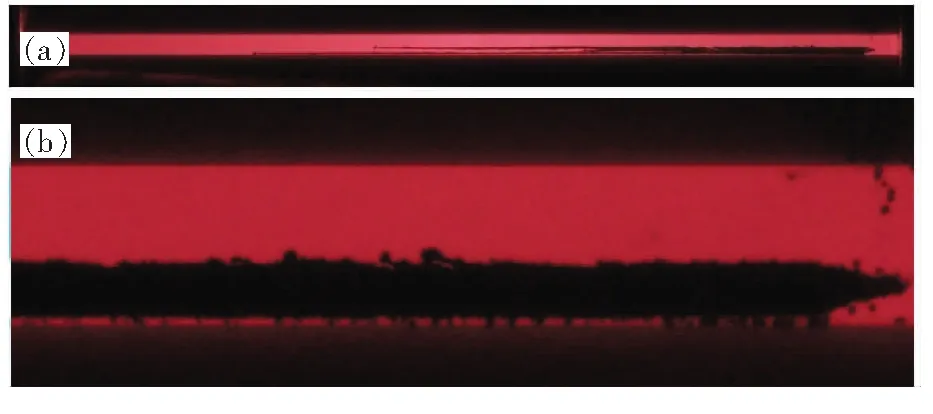
Fig.7 EL images of the COBD near the front facet. (a)EL image of COBD near the front facet (50×). (b)EL image of the front part of the DLDs (200×).
3.2.2 COBD Near The Rear Facet
3 lasers suffered COBD near the rear facets.
Fig.8 shows the EL images of DLDs near the rear facet. The EL image Fig.8(a) shows that the DLDs originate near the rear facet and extend into the active region about 1/3 of the cavity with several branches. Under higher magnification (200×), we can clearly see the DLDs originate from the three points in the vicinity of the rear facet, as the EL image Fig.8(b) presents.

Fig.8 EL images of the COBD near the rear facet.(a)EL image of COBD near the rear facet (50×). (b) EL image of the front part of the DLDs under (200×).
3.2.3 COBD in The Middle of The Bulk
7 lasers suffered COBD in the middle of the bulk.
Fig.9 shows the EL images of DLDs in the middle of the bulk. From the EL image Fig.9(a), it is difficult to confirm the origin of the DLDs. Under higher magnification (200×), we can clearly see the edges of DLDs are large dark regions and it seems that the DLDs tend to extend in <110> direction, as the image Fig.9(b) shows. During the operation, the thermal runaway happens in the middle of the bulk and the dislocations extend along the cavity and expand in <110> direction.

Fig.9 EL images of the COBD in the middle of the bulk.(a) EL image of COBD in the middle of the bulk (50×). (b) EL image of the DLDs in the middle of the bulk (200×).
Among all the 28 lasers that suffered COBD, about 65% of lasers suffered COBD near the front facets, 10% of the lasers suffered COBD near the rear facets, and 25% suffered COBD in the middle of the bulk. Maybe the asymmetric coatings result in the higher optical power in the vicinity of the front facets than the rear facets and the bulk. And due to the non-radiative recombination, more heat is produced near the front facet. Therefore, the COBD tends to happen near the front facet. Moreover, after the COBD happened, the optical power reduced by 30%~90%, corresponding to different damage level.
Different from the COMD, the pre-existing NRCs or specific type of point defects in the active region are the most likely root causes of COBD. During the operation, the NRCs and point defects accumulate. Non-radiative recombination makes defects migrate, react, and dissociate, namely recombination enhanced defect reaction (REDR). Together with filamentation and self-focusing of light, resulting in the increasing local temperature. When the local temperature reaches the critical point, the COBD will occur.
After describing and analyzing the three typical COBD modes, there are some suggestions to suppress COBD process:
1.Developing new materials, such as Al-free material and material with band gap that show low dependence on temperature.
2.Designing new structures, to optimize the optical power distribution and heat distribution profile.
3.Optimizing the epitaxy growth conditions, to obtain high quality interfaces, thus reducing the inter-diffusion, NRRCs, misfit stress, and thermal resistance.
In addition, to obtain higher power and more reliable laser diodes we should:
1.Develop new metal alloy and refine the alloy process condition, to reduce the electrical and thermal resistance, thus lessening the joule heat and improving the heat conducting condition.
2.Introduce new solder, submount and heat-sink, to reduce the strain and improve the thermal conduction condition.
3.Refine the fabrication process, including the lithography, etch, polish,etc, to reduce the contaminations and defects.
4 Conclusion
In this paper, the suddenly failed 975 nm SQW-SCH diode lasers were investigated by performing the electroluminescence. We found that the COD can happen in the bulk without any damage at both facets, guiding our further improvement. The EL images reveal that the dark line defects (DLDs) may originate from the facets (COMD) and the bulk (COBD). And the features of the DLDs of two typical COD modes were interpreted and compared. Furthermore, the causes to the three COD modes are analyzed. And we make some suggestions about suppressing the COD process and further refining the high-power laser diodes.
[1] 王鑫, 王翠鸾, 吴霞, 等. GaAs基高功率半导体激光器单管耦合研究 [J]. 发光学报, 2015, 36(9):1018-1021.
WANG X, WANG C L, WU X,etal.. Coupling research of high power single GaAs based semiconductor laser [J].Chin.J.Lumin., 2015, 36(9):1018-1021. (in Chinese).
[2] HENRY C H, PETROFF P M, LOGAN R A,etal.. Catastrophic damage of AlxGa1-xAs double-heterostructure laser material [J].J.Appl.Phys., 1979, 50(5):3721-3732.
[3] HEMPEL M, TOMM J W, MATTINA F L,etal.. Microscopic origins of catastrophic optical damage in diode lasers [J].IEEEJ.Select.Top.Quant.Electron., 2013, 19(4):1500508.
[4] SOUTO J, PURA J L, TORRES A,etal.. Catastrophic optical damage of high power InGaAs/AlGaAs laser diodes [J].MicroelectronicsReliability, 2016, 64:627-630.
[5] 王文知, 井红旗, 祁琼, 等. 大功率半导体激光器可靠性研究和失效分析 [J]. 发光学报, 2017, 38(2):165-169.
WANG W Z, JING H Q, QI Q,etal.. Reliability test and failure analysis of high power semiconductor laser [J].Chin.J.Lumin. 2017, 38(2):165-169. (in Chinese).
[6] SIN Y, LINGLEY Z, PRESSER N,etal.. Catastrophic optical bulk damage in high-power InGaAs-AlGaAs strained quantum well lasers [J].IEEEJ.Select.Top.Quant.Electron., 2017, 23(6):1-13.
[7] JIMENEZ J. Laser diode reliability: crystal defects and degradation modes [J].ComptesRendusPhysique, 2003, 4(6):663-673.
[8] VANZI M, BONFIGLIO A, MAGISTRALI F,etal.. Electron microscopy of life-tested semiconductor laser diodes [J].Micron, 2000, 31(3):259-267.
[9] TAKESHITA T, SUGO M, SASAKI T,etal.. Failure analysis of InGaAs/GaAs strained-layer quantum-well lasers using a digital OBIC monitor [J].IEEETrans.ElectronDev., 2006, 53(2):211-217.
[10] MARTIN-MARTIN A, AVELLA M, INIGUEZ M P,etal.. A physical model for the rapid degradation of semiconductor laser diodes [J].Appl.Phys.Lett., 2008, 93(17):171106.
[11] QIAO Y B, FENG S W, XIONG C,etal.. Spatial hole burning degradation of AlGaAs/GaAs laser diodes [J].Appl.Phys.Lett., 2011, 99(10):103506.
[12] 井红旗, 仲莉, 倪羽茜, 等. 高功率密度激光二极管叠层散热结构的热分析 [J]. 发光学报, 2016, 37(1):81-87.
JING H Q, ZHONG L, NI Y X,etal.. Thermal analysis of high power density laser diode stack cooling structure [J].Chin.J.Lumin., 2016, 37(1):81-87. (in Chinese)
[13] NAKWASKI W. Thermal-model of the catastrophic degradation of high-power stripe-geometry GaAs/(AlGa)As double-heterostructure diode-lasers [J].J.Appl.Phys., 1990, 67(4):1659-1668.
[14] SOUTO J, PURA J L, JIMENEZ J. About the physical meaning of the critical temperature for catastrophic optical damage in high power quantum well laser diodes [J].LaserPhys.Lett., 2016, 13(2):6.
[15] MENZEL U. Self-consistent calculation of facet heating in asymmetrically coated edge emitting diode lasers [J].Semicond.Sci.Technol., 1998, 13(3):265.
[16] NI Y X, MA X Y, JING H Q,etal.. Finite element analysis of expansion-matched submounts for high-power laser diodes packaging [J].J.Semicond., 2016, 37(6):76-80.
[17] HEMPEL M, TOMM J W, ZIEGLER M,etal.. Catastrophic optical damage at front and rear facets of diode lasers [J].Appl.Phys.Lett., 2010, 97(23):231101.
猜你喜欢
军事文摘(2024年4期)2024-03-19 09:40:02
汽车观察(2021年4期)2021-05-10 05:13:56
汽车观察(2021年4期)2021-05-10 05:12:32
汽车观察(2021年11期)2021-04-24 21:34:38
科学(2020年6期)2020-02-06 09:00:06
电子制作(2019年16期)2019-09-27 09:34:46
车迷(2019年10期)2019-06-24 05:43:06
北京航空航天大学学报(2017年3期)2017-11-23 05:14:28
光学精密工程(2016年5期)2016-11-07 09:06:14
工业设计(2016年4期)2016-05-04 04:00:27