模板法制备CdSe纳米材料及其光电性能
王宏智 雷献超 陈雄卓 姚素薇 张卫国
模板法制备CdSe纳米材料及其光电性能
王宏智 雷献超 陈雄卓 姚素薇 张卫国*
(天津大学化工学院,杉山表面技术实验室,天津 300350)
采用电化学沉积法,在阳极氧化铝(AAO)模板中成功制备出CdSe纳米管和纳米线。利用扫描电子显微镜(SEM)、透射电子显微镜(TEM)、X射线衍射分析(XRD)和能量色散X射线光谱仪(EDS)对材料的形貌、结构和元素组成进行了表征。借助紫外-可见吸收光谱等对材料光催化活性进行了研究。结果表明:通过控制沉积电量可成功制备CdSe纳米管和纳米线;CdSe纳米材料为立方晶型与六方晶型的混合,经350℃退火处理后,CdSe纳米材料中由立方晶型向六方晶型转变,光照开路电位差值明显增强,在0 V(vs SCE)电位下的光照电流密度也有所提高,光电转换性能增强;CdSe纳米线的吸收边在710 nm左右,禁带宽度约为1.85 eV,CdSe纳米管相对于CdSe纳米线具有更高的光电转换性能和光催化活性,经7 h光照后,罗丹明B降解效率高达53.93%。另外,本文还讨论了CdSe纳米材料在AAO模板孔壁的生长机理。
CdSe纳米材料;退火;光催化;电沉积
0 Introduction
Semiconductor materials of metal selenides,such as CdSe and ZnSe,have been widely applied in optics and manufacturing of optoelectronic devices[1]due to their unique electronic properties and optical performance.The erratic properties in nanostructures have attracted great interest in recent decades.Among sulphides and selenides compounds,CdSe,theⅡ~Ⅵgroup semiconductor is one of the most important materials by virtue of its optimum band-gap energy[2].CdSe is a n-type semiconductor with a direct band gap of 1.74 eV for the hexagonal or cubic crystal phase[3].Having an optimum band gap for the efficient absorption and conversion of solar energy,CdSe is a promising photovoltaic material and photocatalyst for photodegradation of organic pollutants[4].In addition,it also has a broad application prospects in the field of solar cells and light-emitting devices[5-6].CdSe onedimensional semiconductor materials such as nanoparticles,nanowires,nanorods and nanotubes can be fabricated by sol-gel method,electrochemical deposition,template synthesis,hydrothermal method and chemical precipitation[7-11].Among various morphologies of nanostructures,CdSe nanotubes are of great interest because ofthe following advantages:The large specific surface area,a direct pathway to transfer charge carriers to the conductive substrate,efficient light absorption and strong adsorption ability[12].Particular attentions have been paid to the fabrication of CdSe nanotubes with the aid of templates.In 2013,Bocchetta et al. successfully fabricated CdSe nanotubes with a length of 700 nm by one-step electrochemical technique of cyclovoltammetric method in anodic alumina membranes (AAO)[13].In 2013,Zhu and Li synthesized CdSe nanotube arrays using ZnO nanorod template on indium tin oxide(ITO)glass[14].
In this study,a potentiostatic potential deposition method was found to fabricate CdSe nanomaterials in the pores of the AAO template with the diameter of 100 nm in an aqueous solution.This method had never been used before for the synthesis of CdSe nanotube(NT)and nanowire(NW)arrays.The structures,morphologies,performance of photoelectric conversion and photocatalytic properties were also discussed in this paper.
1 Experimental
1.1 Materials
All of the reagents used in this work are of analytical grade without further purification.Suppliers of main reagents are listed as below:Industrial Co.,China:SeO2.Tianjin Guangfu Technology Development Co.,Ltd,China:aluminium,oxalic acid,sulfuric acid,phosphoricacid,glycerol,acetone,ethanol,chromium trioxide,EDTA-2Na,CdCl2·2.5H2O,NaOH,NH4Cl and ammonia.Zhongjingkeyi Technology Co.,Ltd:conductive silver glue.Deionized and doubledistilled water were used in all experiments.
1.2 Preparation of CdSe nanomaterials
The AAO template was fabricated by a two-step anodization process with the method described in the reference[15-16].A layer of Au film was sprayed onto one side of the through-hole AAO template for the working electrode.A conventional three-electrode potentiostatic system was used for cathodic deposition of CdSe nanoparticles.Saturated calomel electrode (SCE)and a platinum plate were used as the reference and counter electrodes.CdSe nanomaterials were electrodeposited into the AAO/Au template in an aqueous solution containing 0.01 mol·L-1CdCl2·2.5H2O,0.02 mol·L-1EDTA-2Na and 0.02 mol·L-1SeO2(pH=10 adjusted by NH4Cl and ammonia).The deposition was carried out potentiostatically at-1.1 V versus the reference electrode at room temperature.After deposition,the sample was rinsed with DI water and dried in air.Finally,the CdSe nanomaterials were annealed at 350℃for 2 h under N2atmosphere.By controllingthedeposited charge,wesuccessfully fabricated different morphologies of CdSe materials.
1.3 Characterization of CdSenanomaterials
The morphologies of CdSe nanomaterials were studied through scanning electron microscopy(SEM,S-4800,HITACHI,Japan).Detailed microscopic structure and chemical composition of the materials were characterized by transmission electron micros-copy(TEM,JEM-2100,JEOL,Japan).The crystalline structure of CdSe nanomaterials was studied by X-ray diffraction (XRD,40 kV,200 mA,Rigaku,Mutiflex,D/MAX-2500,Japan)under Cu Kα radiation (λ =0.154 056 nm)with 2θ range of 20°~70°.Chemical compositions of the material were analyzed using energy dispersive X-ray spectroscopy(EDS).Curves of open circuit potential and photocurrent versus potential were conducted at electrochemical workstation with three-electrode system under a 500 Xe lamp.CdSe NTs and CdSe NWs(1 cm×2 cm)served as the working electrode,while a platinum plate electrode and an SCE were used as the counter and reference electrodes respectively in separate compartment filled with an aqueous electrolyte solution of 0.5 mol·L-1Na2SO4.The difference of open circuit potential(Voc)was calculated via Voc=|Vlight-Vdark|,where Vlightis the potential when light was on and Vdarkmeans the light was off.UV-visible absorption spectra of the samples were recorded on a spectrometer(TU-1901,PERSEE,China).
1.4 Photocatalytic activity measurements
Photocatalytic degradation was carried out in 100 mL of 5 mg·L-1rhodamine B solution under a 500 W Xe lamp (290~800 nm).As needed,the solution was magnetically stirred in the dark for 2 h prior to irradiation to ensure the establishment of an adsorptiondesorption equilibrium of the rhodamine B molecules on the photocatalyst.The change in concentration during the degradation process was monitored by a UV-Vis spectrophotometer based on its characteristic absorbance at 554 nm every 1 h.The photocatalysis degradation efficiency(D)was calculated by means of D=(C0-C)/C0×100%,where C0is the initial concentration of rhodamine B in the solution and C is the concentration of rhodamine B at a given reaction time.In order to obtain the specimen for tests all above,samples were dissolved in a 4 mol·L-1NaOH solution for 2 h at room temperature.
2 Results and discussion
2.1 Characterization of CdSe nanomaterials
Fig.1(a)shows the SEM image of AAO template.The pore diameter of the uniformed AAO template is approximately 100 nm.Fig.1(b),(c)and(d)show the SEM image of CdSe nanomaterials after the removal of AAO template with thedeposited charge of1 coulomb,3 coulombs and 5 coulombs,respectively.Fig.1(b)shows the SEM image of CdSe NTs with the deposited charge of 1 coulomb.It can be clearly observed that the external diameter and wall thickness of the nanotubes are about 100 nm and 20 nm,respectively,which are corresponding to the pore diameter of AAO template.In Fig.1(c),it is apparent that a number of CdSe NTs come into being CdSe NWswith thedeposited charge increased from 1coulomb to 3 coulombs.Fig.1(d)shows that the CdSe NTs completely grow into CdSe NWs which are distributed uniformly with the diameter of 100 nm.
Fig.1(e)and Fig.1(f)show TEM images of CdSe NTs and CdSe NWs,respectively.Distinct tubular and linear structures can be seen in TEM images.In Fig.1(e),the external diameters and wall thicknesses of the NTs are about 100 nm and 20 nm,respectively,which are in agreement with the SEM observations in Fig.1(b).From both Fig.1(e)and Fig.1(f),it also can be seen that the CdSe NTs and CdSe NWs are straight and have the uniform thickness along the length.
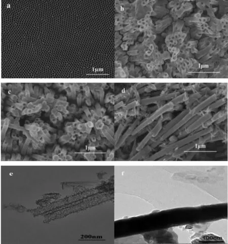
Fig.1 SEM images:AAO(a)CdSe nanomaterials(b,c,d)and TEM images of CdSe(e,f)
The characteristic peaks of Cd,Se,Ag are marked in the EDS spectrum of CdSe nanomaterials,as shown in Fig.2,indicating the material is composed of these elements.The average atomic percentage of Cd and Se is close to 1∶1 indicated in Table 1.Ag signals come from silver plastic on the electrode。
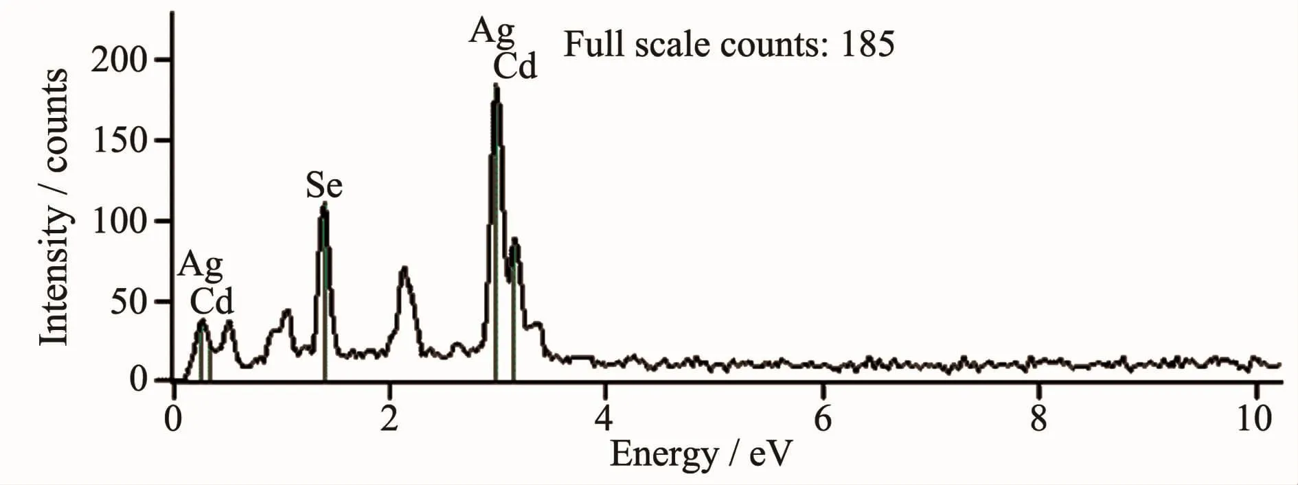
Fig.2 EDS spectrum of CdSe nanomaterials

Table 1 Mass distribution and atomic distribution of each element in Fig.2
2.2 Effect of annealing
The effect of annealing on crystallinity of CdSe nanomaterials were studied by XRD.Fig.3 shows the XRD patterns of CdSe NTs and CdSe NWs asdeposited(a)and annealed at 350℃(b).Fig.3(a)indicates the existence of mixed phase nature of hexagonal and cubic of CdSe NTs and CdSe NWs.The diffraction peaks observed at 2θ values of 25.48°,42.21°,49.96°and 67.42°can be indexed to(111),(220),(311)and(331)crystalline planes of cubic CdSe crystal (PDF 65-2891),respectively.The diffraction peaks at 2θ values of 23.90°,27.08°,35.11°,41.97°and 45.79°can be indexed to(100),(101),(102),(110)and(103)crystalline planes of hexagonal CdSe crystal(PDF 08-0459).It can be seen in Fig.3(b)that both crystal transformation of CdSe nanotubes and nanowires from the cubic phase to the hexagonal phase after the annealing process at 350℃[17].The diffraction peaks at 2θ values of 23.90°,27.08°,35.11°,41.97°,45.79°,49.67°and 63.88°can be indexed to(100),(101),(102),(110),(103),(112)and(203)crystalline planes of hexagonal CdSe crystal(PDF 08-0459).

Fig.3 XRD patterns of CdSe nanomaterials as-deposited(a)and annealed at 350℃(b)
The effect of annealing on photoelectrochemical properties of CdSe nanomaterials is characterized by measuringopen-circuitpotentialand photocurrent versus potential.Fig.4 and Fig.5 show the open-circuit potential curves of CdSe nanomaterials as-deposited(a)and annealed at 350℃(b)measured under dark or light.As shown in Fig.4,CdSe NTs(a)and(b)show significant potential decrease when the light irradiates onto the samples.The open-circuit potential difference(Voc)of CdSe NTs before and after annealing are about 90.6 and 191.3 mV,respectively.In Fig.5,the opencircuit potential difference(Voc)of CdSe NWs before and after annealing are about 63.3 and 162.9 mV,respectively.The results show that the annealing process effectively increases the open-circuit potential difference(Voc)of CdSe nanomaterials,which may result from crystal transformation of CdSe from the cubic phase to the hexagonal phase induced by heat treatment at 350℃.Furthermore,the CdSe NTs before and after annealing both exhibit a higher open-circuit potential difference(Voc)than CdSe NWs,indicating that the photo-induced carriers can easily transfer from the nanotubes with larger specific surface area.As a result,CdSe NTs annealed at 350℃have a better photoelectric conversion performance for large specific surface area and good crystallinity.
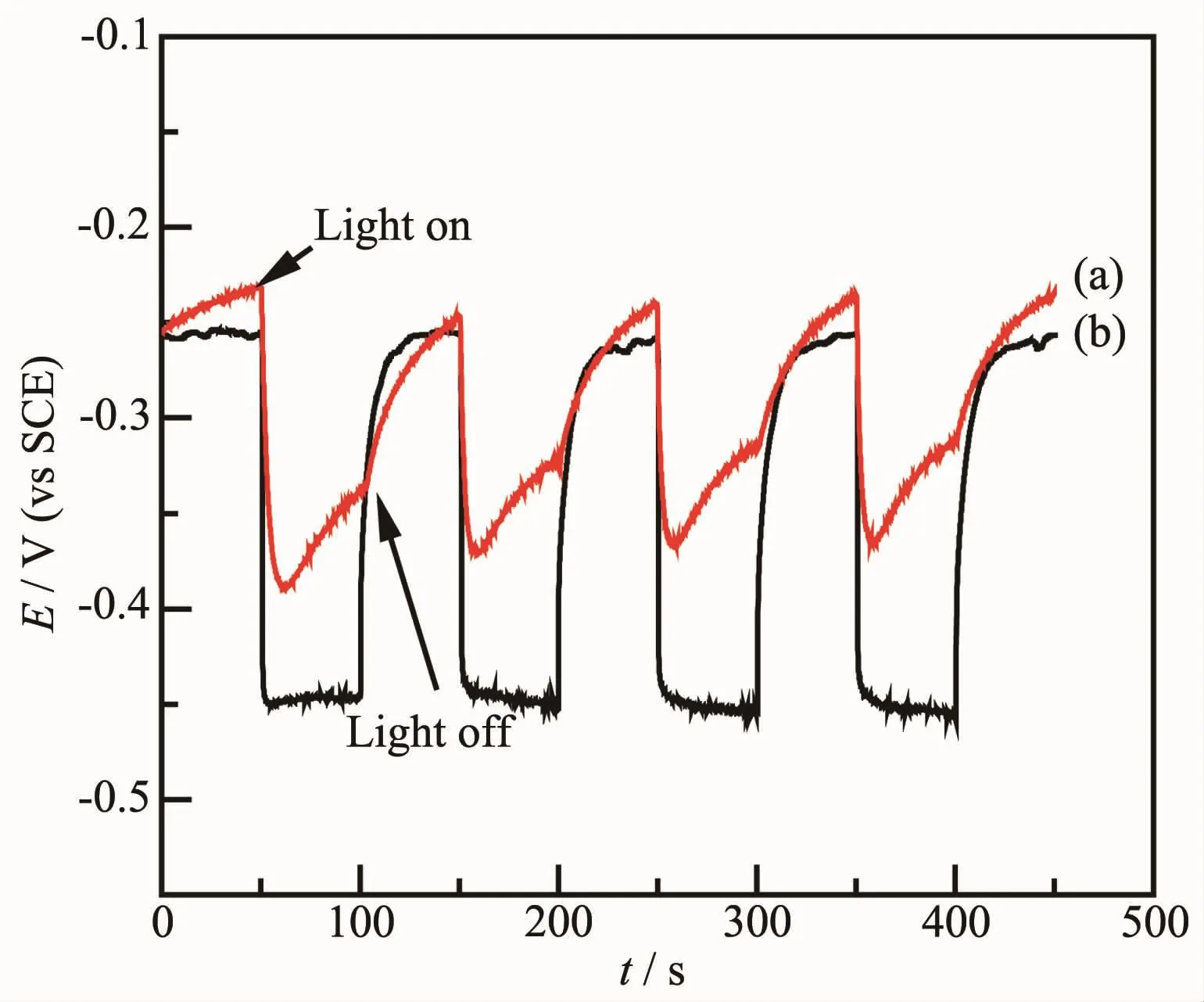
Fig.4 Open-circuit potential curves of CdSe NTs:(a)as-deposited,(b)annealed at 350℃

Fig.5 Open-circuit potential curves of CdSe NWs:(a)as-deposited,(b)annealed at 350℃
Fig.6 shows the current density-potential(J-V)curves of the samples.All the samples show negligible currentunder dark condition.The photocurrent density of CdSe nanotubes(NTs)and nanowires(NWs)annealed at 350℃ (b)are about 0.12 and 0.99 mA·cm-2at 0 V versus SCE,both show higher photoelectrochemical properties than those as deposited under illumination.The improved performance is attributing to the crystal transformation of CdSe after heat treatment at 350℃.The same as the open-circuit potential difference(Voc),the photocurrent of CdSe NTs before and after annealed both improve the performance than those of CdSe NWs due to their large surface area.
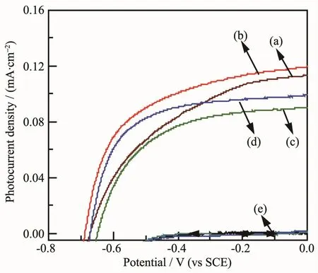
Fig.6 Photocurrent density versus potential curves(a)CdSe NTs as-deposited,(b)CdSe NTs annealed,(c)CdSe NWs as-deposited,(d)CdSe NWs annealed,(e)dark current
2.3 UV-Vis spectroscopy
Fig.7(a)shows the UV-visible absorption spectrum of the CdSe nanowires.It is observed that the absorption edge of CdSe nanowires is about 710 nm,a wide absorption in visible region[18].Fig.7(b)shows the corresponding band gap of samples.The band gap of CdSe nanowires is about 1.85 eV.Which is in accordance with the band gap of CdSe NWs previously reported[19].
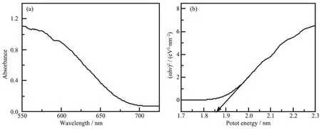
Fig.7 (a)UV-Vis absorption spectra of CdSe nanowires and(b)band gap of CdSe nanowires
2.4 Photocatalytic activities
Fig.8 shows the degradation rate of rhodamine B catalyzed by CdSe nanotubes(a),CdSe nanowires(b),and without catalyst(c)under the Xe lamp irradiation.The blank test was conducted without catalyst under irradiation for the same time.The results indicate that the degradation rate of rhodamine B is only 10.83%after irradiation for 7 h,which presents the stability of rhodamine B solution under irradiation.After irradiation for 7 h,the degradation rates of rhodamine B have been increased to 53.93%and 47.14%in the presence of CdSe nanotubes and CdSe nanowires,respectively.The results reveal that CdSe nanotubes display much better photocatalytic activity than CdSe nanowires.The enhancement of photocatalytic activities is mainly attributed to larger specific surface area and high migration efficiency of photo induced electrons of nanotubes than nanowires.
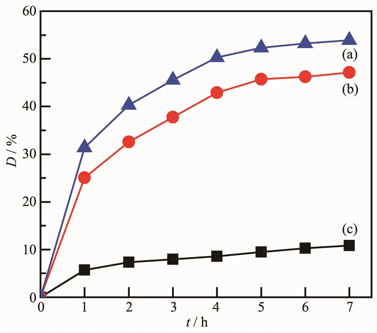
Fig.8 Photocatalytic performances of CdSe nanotubes(a),CdSe nanowires(b),and without catalyst(c)
2.5 Mechanism of formation of CdSe nanomaterials
According to the basic mechanism of electrochemical reactions[20], we speculated that possible processes maybe occur during the electrodeposition.The reactions may be summarized as follows:


The growth mechanism of CdSe nanotubes in the pore walls of AAO template can be speculated that it may be determined by the relative rates of deposition and the diffusion of ions[21-22].During the growth process of nanotubes,reaction(1)~(3)occur at the sputtered Au electrode at the bottom of AAO pores and then reacts with Cd2+.therefore,the growth of CdSe nanotubes starts at the sputtered annular Au base-metal electrode at the bottom of the pores.Deposition interface and ion diffusion layer move dynamically with the nanotube growth process.In the growth process of CdSe nanotubes,the deposition of CdSe onto the AAO tube tips can deplete the Cd2+ions in the same layer,so the ion concentration below the tube tips should be very low.In the nanochannel,the rate of Cd2+diffusion is very small due to the narrowlong structure of AAO template.So,the deposition of CdSe into the inner walls of the CdSe tube can be negligible.Therefore,the deposition reaction could occur only in the annular tips of AAO template.Owing to the deposition of CdSe proceeds along the inner wall of porous AAO template,CdSe nanotube walls become thicker with the increase of deposition charge and until completely form CdSe nanowires.
3 Conclusions
In summary,different morphologies ofCdSe nanomaterials have been successfully fabricated with electrodeposition method in the aid of AAO template by controlling the deposite charge.The growth mechanism of CdSe nanomaterials in the pore walls of AAO template may be determined by the relative rates of deposition and the diffusion of ions.It is assumed that the process of annealing effectively induces the crystal transformation from the cubic phase to the hexagonal phase.Furthermore,the results ofopen-circuitpotentialand photocurrentversus potential show that both CdSe nanotubes and CdSe nanowiresannealedat350℃exhibitbetter photoelectric conversion performance,indicating that theCdSe ofhexagonalphase hasmuch better photoelectric conversion performance than the cubic phase.Photodegradation experiment shows that the nanotube arrays have a good photocatalytic capability.
[1]Sholin V,Breeze A J,Anderson I E,et al.Sol.Energy Mater.Sol.Cells,2008,92(12):1706-1711
[2]Cumberland S L,Hanif K M,Javier A,et al.Chem.Mater.,2002,14(4):1576-1584
[3]Kainthla R C,Pandya D K,Chopra K L.J.Electrochem.Soc.,1980,127(2):277-283
[4]Grunwald M,Lutker K,Alivisatos A P,et al.Nano Lett.,2012,13(4):1367-1372
[5]Jander S,Kornowski A,Weller H.Nano Lett.,2011,11(12):5179-5183
[6]Lee H J,Wang M,Chen P,et al.Nano Lett.,2009,9(12):4221-4227
[7]Lieber C M.MRS Bull.,2011,36(12):1052-1063
[8]Ma C,Wang Z L.Adv.Mater.,2005,17(21):2635-2639
[9]Miao Z,Xu D,Ouyang J,et al.Nano Lett.,2002,2(7):717-720
[10]Arachchige I U,Brock S L.J.Am.Chem.Soc.,2006,128(24):7964-7971
[11]Zhang Q,Guo X,Huang X,et al.Phys.Chem.Chem.Phys.,2011,13(10):4659-4667
[12]Epifani M,Giannini C,Manna L.Mater.Lett.,2004,58(19):2429-2432
[13]Bocchetta P,Santamaria M,Di Quarto F.Electrochim.Acta,2013,88:340-346
[14]Xie Y,Wei L,Wei G,et al.Nanoscale Res.Lett.,2013,8(1):1-6
[15]Song Z,Xie Y,Yao S,et al.Mater.Lett.,2011,65(1):44-45
[16]Wang H,Liu N,Lu J,et al.Chem.Res.Chin.Univ.,2015,31(5):846-850
[17]Drndic'M,Jarosz M V,Morgan N Y,et al.J.Appl.Phys.,2002,92(12):7498-7503
[18]Mahato S,Shakti N,Kar A K.Mater.Sci.Semicond.Process.,2015,39:742-747
[19]XU Zhe(徐哲),XUE Jin-Bo(薛晋波),YANG Hui-Juan(杨慧娟),et al.Chinese J.Inorg.Chem.(无机化学学报),2016(4):589-594
[20]Fan H J,Werner P,Zacharias M.Small,2006,2(6):700-717
[21]Lee W,Scholz R,Nielsch K,et al.Angew.Chem.Int.Ed.,2005,117(37):6204-6208
[22]Wang H,Song Y,Liu W,et al.Mater.Lett.,2013,93:319-321
Template Synthesis and Photoelectrochemical Properties of CdSe Nanomaterials
WANG Hong-ZhiLEI Xian-Chao CHEN Xiong-ZhuoYAO Su-WeiZHANG Wei-Guo*
(Sugiyama Laboratory of Surface Technology,School of Chemical Engineering and Technology,Tianjin University,Tianjin 300350,China)
CdSe nanotube and nanowire arrays have been fabricated in the porous anodic aluminum oxide template(AAO)by electrodeposition method.The morphology,structure and composition of the materials were characterized by scanning electron microscopy (SEM),transmission electron microscopy (TEM),X-ray diffraction (XRD)and energy dispersive X-ray spectroscopy (EDS)respectively.The photocatalytic activities of the materials were investigated by UV-vis absorption spectroscopy.The results show that CdSe nanotube and nanowire arrays can be fabricated by controlling the deposited charge.The CdSe nanomaterials are composed of mixed phase nature of hexagonal and cubic phase.It can be observed that the crystal transformation from the cubic phase to the hexagonal phase after the annealing process at 350℃.Meanwhile,the open-circuit potential differences(Voc)of the annealed CdSe nanomaterials have significantly increased,and photocurrent density at 0 V(versus SCE)has also improved,indicating that the annealed nanomaterials show better photoelectrochemical properties.Furthermore,the absorption edge and band gap of CdSe nanowires are about 710 nm and 1.85 eV respectively,CdSe nanotube arrays exhibit a better photoelectrochemical performance and a higher activity than nanowires for photodegrading rhodamine B with the degradation efficiency of 53.93%under a Xe lamp irradiation for 7 h.In addition,the growth mechanism of CdSe nanomaterials in the pore walls of AAO template has also been discussed.
CdSe nanomaterials;anneal;photocatalysis;electrodeposition
O614.24+2
A
1001-4861(2017)12-2271-07
10.11862/CJIC.2017.264
2017-02-21。收修改稿日期:2017-09-10。
天津市自然科学基金(No.11JCYBJC01900)资助项目。
*通信联系人。 E-mail:zwg@tju.edu.cn

