Energy Estimation and Optimization Platform for 4G and the Future Base Station System Early-Stage Design
Wei Wang, Dake Liu, Ying Zhang, Chen Gong
Lab of Application Specific Instruction-set Processors, Beijing Institute of Technology, Beijing 100081, Beijing, China
* The corresponding author,email: dake@bit.edu.cn
I. INTRODUCTION
Energy savings have been a driver for standardization of cellular networks like LTE-Advance [1] and the 5G mobile communication network [2]. Base station energy/power consumption modeling [3-9] at system level is an essential research. However, most of existing power/energy models have not yet provided instrumental energy/power estimation for system designers in early design stages. This is because existing models greatly depend on detailed physical information of commercial-offthe-shelf (COTS) components. Such COTS information may be unavailable or insufficient in early design stages.
On the one hand, in [5,8,9], GIPS-based(giga instructions per second) method is proposed for power estimation of digital baseband subsystem (DBB). The detailed physical information here refers to the power to performance ratio of an available processor and the number of instructions involved in each physical layer algorithm. This physical information is used for power estimation of each algorithm. However, if there is no available processor for new system design in early stages, GIPS-based method will not be feasible due to the lack of the physical information. The as-yet unstan-dardized 5G is such an example.
In this paper, a holistic power/energy estimation model is proposed for base station system early-stage design.
On the other hand, in [3-6], measured power values of all analog subsystems except PA,are simply used for power estimation. However, base station design is usually highly customizable. The measured values may not be suitable in other cases. Generic analog component power models are nevertheless necessary in system design for power budget, to select suitable components and to identify low-power design opportunities in early design stages.
Therefore, this paper motivates the needs for modeling energy and power consumption of new generation base station designs with insufficient physical information. A cross-platform DBB energy model is proposed for energy estimation of new system design, which is strongly inspired by block reuse [10]. With the physical information from reuse blocks,energy consumption of other new design blocks in target system can be estimated. Our fine-grain energy model focuses not only on energy estimation, but also on evaluating and optimizing energy/power consumption of candidate system designs in early design stages.Consequently, an energy optimization method based on the DBB energy model is introduced to explore optimal DBB design alternatives for energy/power minimization. Meanwhile,through collecting power figures from hundreds of published papers, statistical power models of analog subsystems are also presented to capture the variation trend of existing radio frequency (RF), analog-to-digital converter (ADC), and digital-to- analog converter(DAC) designs. In addition, a PA power model is also proposed, which provides more configurable parameters for designers to estimate power consumption of candidate PA designs.
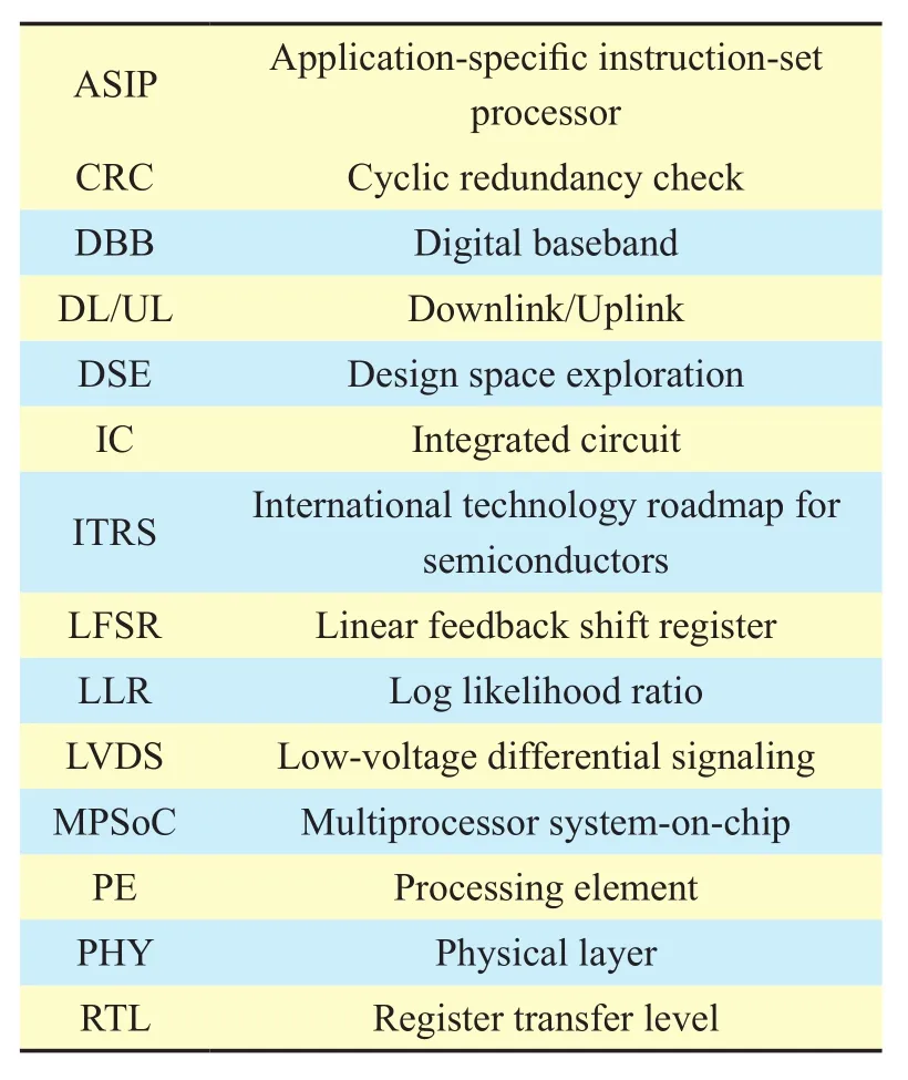
The rest of this paper is organized as follows. In section II, modeling methodology and basics of digital baseband are reviewed and discussed. The generic baseband energy model and analog subsystem power models are presented in section III. A power/energy optimization method combined with a design space construction method for digital baseband design is introduced in section IV. Section V provides an early power estimation case of digital baseband and power amplifier. Section VI concludes this paper. For easy reading, the main abbreviations in this paper are summarized and listed at the end of the paper.
II. MODELING METHODOLOGY
In this section, the DBB energy modeling method and related backgrounds are briefly reviewed.
2.1 Principle and scope
We proposed a hierarchical power model for estimating the IC (integrated circuit) power dissipation of MIMO- OFDM baseband in early design stages [11]. By this model, the power estimation of an algorithm is mainly depended on computing costs (e.g., the number of adders, multipliers, logic gates and memories)mapping on a specific microarchitecture. This power model is suitable for both programmable processors and dedicated hardware.
In this paper, besides the power model, an additional execution time model is also proposed together with the power model as an integrated DBB energy model.
2.2 Modeling basics
According to ITRS report [12], the proportion of design block reuse in new design is 35% in 2007, and it will increase to 58% by 2022. More pre-existing blocks (intellectual property-IP) are applying to new designs to reduce design costs and time-to-market. System level DBB energy model in this paper is thus strongly inspired by block reuse. “Many designs (especially microprocessors) are based on modifications or extensions to existing designs, such a method can provide fairly accurate early estimates” [13]. In other words,though it is a new DBB design, it mostly consists of pre-existing blocks. Thus limited yet predictable physical information from reuse blocks can be used to estimate power consumption and execution time of new design blocks. In this paper, a pre-existing or new design block refers to a physical layer module(e.g., FFT module).
Consequently, these two kinds of blocks are taken into consideration in our DBB model,i.e.,
--Pre-existing blocks (reuse blocks): This paper focuses on heterogeneous multiprocessor system-on- chip (MPSoC) DBB platform,as shown in Figure 1 [14]. Pre-existing blocks here refer to existing microarchitectures of specified algorithms running on digital signal processor (DSP), application specific integrated circuit (ASIC) or field -programmable gate array (FPGA) platforms. Furthermore, implementation details (i.e., physical information) at low-level (register transfer level–RTL and below, e.g., gate-level) can be reused in early design stages, such as data parallel, task parallel,counts of logic gates/macro blocks, memory cost and data access, interconnect information(e.g. the number of metal layers, area, length,power and delay), and data switching activity;
--New design blocks: New design blocks can be divided into two categories: modification of an existing microarchitecture (e.g.,parallelization) and new microarchitecture design. For the latter, we model an early microarchitecture design by using its control and data flow graph (CDFG, it is a directed acyclic graph, the vertices of CDFG represent either arithmetic or logic statements of algorithms, or the control statements. Edges model the data/control flow dependencies.), timing diagram,and target platform (DSP/ASIC/FPGA). Due to the lack of implementation details at low level, energy estimation of new design blocks mainly depends on physical information derived fromreuse blocks.
2.3 Modeling objects and methods
2.3.1 Objects
The following offers details when building our DBB energy model for aforementioned two kinds of blocks.
For every specific physical layer module (e.g., channel estimation module in LTE PHY),
--Algorithm set: Classic and new algorithms are collected for a module and further described as their CDFGs and timing diagrams. For instance, FIR algorithm set includes two basic members at least, i.e., direct form and linear phase algorithms. This method is exposed to designers to build their own algorithm sets.
For each algorithm within an algorithm set,
--Microarchitecture set: According to CDFG and timing diagram of an algorithm, its microarchitecture is selected and/or designed.Data parallel and task parallel structures of a CDFG are explored for designing microarchitecture set.
For power estimation and execution time estimation of each microarchitecture within a microarchitecture set,
--Standard cell/Macro block library: For DSP and ASIC platforms, their smallest unit is standard cell and macro block at RTL. The standard cell is a kind of predesigned sub-circuits such as simple logic gates. The macro block is also a kind of predesigned sub-circuits with regular structure (e.g., multipliers, adders and memories) composed from standard cells.The standard cell/macro block library contains all of the available standard cells and macro blocks with detailed physical information. In terms of the proposed DBB energy model, in order to accurately estimate execution time and power consumption of new design blocks,standard cell/macro block library used in reuse blocks has to be referred. On the other hand,the smallest units in a FPGA are programmable logic elements, not standard cells. A logic element usually consists of lookup tables and registers. FPGA functional modules are composed of such logic elements. Hence, for FPGA-based baseband energy estimation, the logic elements are used in the proposed model.
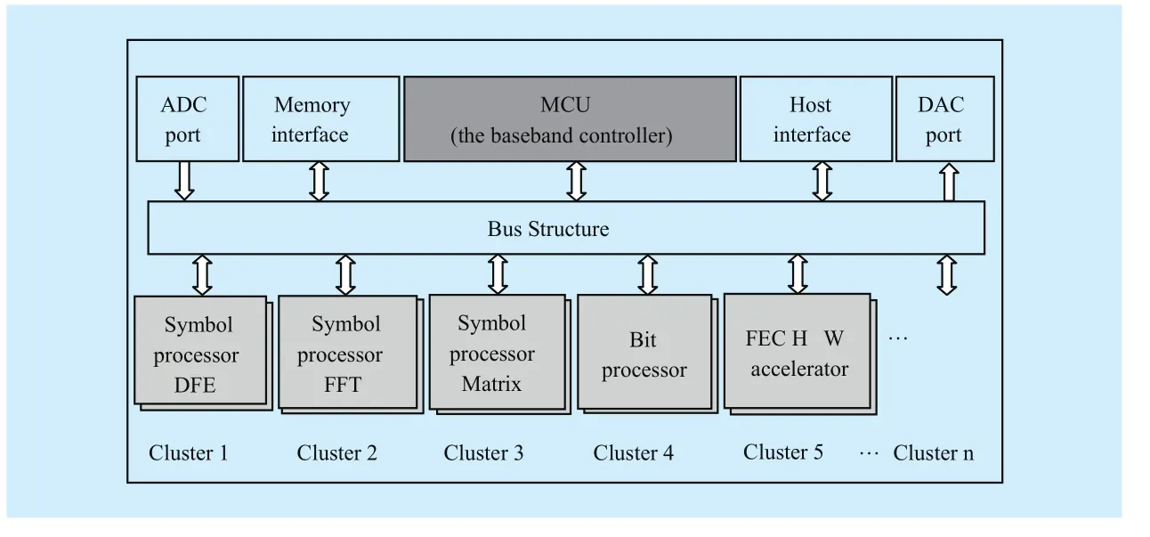
Fig. 1 Heterogeneous digital baseband MPSoC
2.3.2 Methods
Energy estimation for a new design block can be performed in 3 steps:
Step 1–Microarchitecture: A hardware block is built which is based on an algorithm CDFG of a new design block.
Step 2–Hardware: The logic gates, functional macro blocks (e.g., multiplier), and memory access within microarchitecture are counted.
Step 3–Estimation: According to specified physical information extracted from reuse blocks, execution time and power consumption of this microarchitecture can be estimated using the following models.
III. GENERIC MODELS
In [11], the power model of a base station has been formulized as follows:

In this section, integrated DBB energy model and analog subsystem power models,i.e.,EDBB,PRF,PPA,PADC,PDAC, are presented.The power consumption of system level memory buffer (PBuffer), the power supply (PMain Sup-ply), and the backhaul (PBackhaul) largely depend on specific equipment specification.
3.1 Digital baseband energy models
Circuit energy consumption is the product of its average power and execution time (runtime). The power model is thus first introduced, followed with execution time model and the final energy model.
1) The power model
We restructure the power model of [11] in the view of MPSoC illustrated in Figure 1.Note that the power model still focuses on dynamic power.
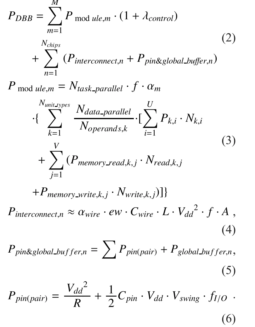
In (2), λcontrolis the overhead ratio of the whole control power including microcontroller(MCU) and part of microarchitecture (e.g.,instruction fetch, instruction decoding, address computing of DSP; finite state machine of ASIC/FPGA).
Pmodule,mis the power dissipation of the physical layer modulem, such as the power dissipation of a sequence of instructions (DSP)or an application-specific integrated circuit(ASIC/FPGA).Mis the total number of PHY modules at base station side. Each module, executed by processing elements (PEs) in Figure 1, can be further modeled in (3).
Ntask_parallel,is the number of enabled PEs within a cluster running the modulem.
f,αmdenote the operating frequency and average data switching activity of all enabled PEs running the modulem, respectively.
Ndata_parallel,is the degree of data parallelism of a PE, andNunit_typesis the number of different types of basic functional units in a PE.Noper-ands,kis the number of operands ofkth (type)basic functional unit in a PE. For instance,suppose the microarchitecture of FFT symbol processor (Figure 1) is with 4-complex data input (Ndata_parallel=4) and consists of two kinds of basic functional units, i.e., radix-2 butterfly and radix-4 butterfly (Nunit_types=2). 1) In terms of radix-2 (Noperands,1=2), there areNdata_parallel/Noperands,1=4/2=2 radix-2 butterflies in this FFT PE. 2) Likewise, there isNdata_parallel/Noper-ands,2=4/4=1 additional radix-4 butterfly in this PE.
Uis the number of distinct types of logic gates/macro blocks (in terms of data precision,etc.) withinkth basic functional unit;Pk,i, Nk,iare the calibrated power and the number of theith (i.e., same type) logic gate/macro block(macro blocks including adder, multiplier,etc.).
Vdenotes the number of memory access times whenkth basic functional unit runs once,Pmemory_read,k,j, Pmemory_write,k,jarethe power dissipation of memory read and write operations respectively. Its power dissipation largely depends on the memory size, memory(bank) width, data type (bit, real data and complex data) and data precision of operands.Nread,k,j, Nwrite,k,jis the iterations ofjth read and write operations, for example, duringkth basic functional unit execution, 2 times memory access happens (V=2), in the first round (j=1),100 bits need to read from local RAM into register file, yet the width of this RAM is 10 bit, as a result this job has to consume 10 read operations, i.e.,Nread,k,1=10,Pmemory_read,k,1is the power consumption of reading 10 bit.
Pinterconnect,ndenotes the interconnect power dissipation in a single chip;Nchipsis the total number of chips. Referring to ITRS report[15], the power of interconnect wires in the chipncan be estimated by (4), where, αwireis the average interconnection wire activity ratio;ewis the wiring efficiency;Cwireis the average capacitance per unit length (including Metal 1, intermedia wires and global wires);Lis the average metal length of Metal 1 and five intermedia levels per unit area;Vddis supply voltage;fis the chip operating frequency;Ais the area of the chipn.
Ppin&global_buffer,nin (5) denotes the total power consumption of pins (including full swing and LVDS pins) and non-functional on-chip global buffer (SRAM) of the chipn. This buffer is used to buffer data from other chips or off-chip memory. Its power (Pglobal_buffer,n) is a custom parameter for target system. The pin driver power consumption (ΣPpin(pair)) of a chip depends on the number of pin/pin-pair and power consumption per pin/pin-pair (Ppin(pair)).Ppin(pair)can be estimated by (6), where,Vddis the driver supply voltage andVswingis the pin voltage swing;Ris the termination resistor;Cpinis the load capacitance;fI/Ois the I/O port frequency.
2) The execution time model
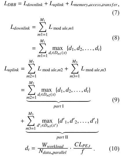
In (7),Ldownlinkdenotes the total execution time of all PHY modules in downlink (DL).This execution time mainly includes computation delay and memory access delay. It can be approximately estimated by formula (8).
M1is the total number of PHY modules in DL.x,dtdenotes the workload and execution time of the PEtwithin a cluster running the modulem1;tis the number of enabled PEs in this cluster and satisfiest<= total number of PEs of this cluster. ThusDm1(x)is a set comprising all availabledt. Furthermore, the maximum value among this set is exactly the execution time of the modulem1. Generally,the maximum time depends on workload allocation on different PEs within a cluster.
Likewise,Luplinkis the execution time of the whole PHY modules in uplink (UL). However, compared to DL, a difference of UL (9) is the coexistence of user-shared modules (m2in part I, the same asLdownlink) and user-specific modules (m3in part II). For instance, in LTE/LTE-A uplink, FFT is a user-shared module processing symbols of the whole transmission bandwidth and all users. Rather, IFFT is user-specific module since its workload is only for partial transmission bandwidth, i.e. a user’s bandwidth.
M2,M3are the number of user-shared modules and user-specific modules, respectively. It is important to note thatx’in part II is possibly a collected workload of multi-users when the number of users is more than the number of available PEs in a cluster. For example,suppose there are two processors in cluster 2(Figure 1) and three users in uplink; PE 1 may process the data of user 1 and PE 2 may process the data of user 2 and 3, thend’1, d’2is the computing delay of PE 1 and PE 2 with the workloadx’1(user 1),x’2(combination of user 2, 3) respectively.
Lmemory_access_transferis the average time cost for data access between two chips or between the off-chip main memory and on-chip PE memory transfers e.g., direct memory access(DMA), which is largely depended on specific MPSoC structure design, such as main memory or PE position, bus structure, etc.
In practice, the execution time of a specific PE can be calculated by (10),Wworkloadis the allocated workload of the PEt;Ndata_parallel,is the degree of data parallelism of PEt;CLPE,tdenotes the clock cycles consumed by PEtforNdata_paralleldata processing;fis clock frequency. Let us take CRC as an example; the original microarchitecture of CRC is linear feedback shift register (LFSR). Since data parallel cannot be applied on LFSR,Ndata_paral-lel=1. In other words, it computes one input bit per clock cycle, i.e.,CLPE,t=1 cycle. Suppose current workload of the PEtis 6144 bit andf=100MHz, then its execution time can be roughly estimated by (10),

The runtime is obviously too long. Improvements and runtime minimization of CRC are discussed at the step 2 in section 5.1.1 of this paper.
3) The energy model
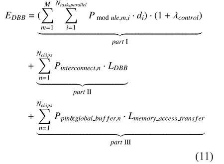
where, part I is the energy dissipation of all clusters and the MCU;di,Pmodule,m,iare the execution time and power consumption of the PEiin clustern(Figure 1) running the PHY modulem; part II, III is the energy consumption of interconnect and non-functional memory access of all chips respectively.
3.2 Analog component power models
We propose statistical power models for RF,DAC and ADC [16] by investigating several hundreds of published papers (from 1994 to 2016). These models can provide a clear picture of current situation and future trend of RF, DAC, and ADC power consumption for designers.
3.2.1 RF
The RF power model in form is,

where, δtechnologyis technology scaling factors(With the development of silicon technology,the value of δtechnologyis not a constant. Consequently, both old references and recent papers of RF design cases need to be collected to capture the range of δtechnologyand create the predictable statistical model);Vconstantis DC(direct current) bias voltage;Vddis supply voltage;Vswingis the RF voltage swing. The voltage used for measuring the values of all parameters except θiin the brackets is 1 volt.Pbasedenotes the base power value within 1 MHz bandwidth at 1 GHz, IIP3=10 dBm and sensitivity=-20 dBm (actually, designers can intentionally choose the baseline of bandwidth, frequency, IIP3 (third-order intercept point) and sensitivity);fcis carrier frequency;δbandwidth,δIIP3,δsensitivityare RF parameters of bandwidth, IIP3, and sensitivity; θi,i=0,1,2,3,are corresponding weight factors;gi(·),i=0,1,2,3, are the mapping functions fromfc,δbandwidth,δIIP3and δsensitivitytoPRF;PFSis the power of frequency synthesizer.
We collected up to 600 published papers and selected more than 200 useful papers for θiregressions without normalization, as illustrated in Figure 2,3,4,5. Regression models can be further created by using the overall data,e.g.,p(1)RF(green line) in Figure 3, and partial data, e.g., bandwidth>100 MHz, is selected to generatep(1)RF(red line) to roughly predict RF power dissipation of wide bandwidth system.Finally, designers should make a decision on reference values offc, δbandwidth,δIIP3, andδsensi-tivityof a target RF design and thus early power estimation can be calculated by using (12).It is important to note that the estimation accuracy of statistical RF circuit power models largely depends on the number of data and the selection of fitting functions. Several kinds of fitting functions were selected in Figure 2,3,4,5 to show a case of building statistical models, and designers should test goodness of fit by using their own selected data to select appropriate fitting functions.
3.2.2 PA
In this paper, several impact factors on PA efficiency are investigated to provide more chances for designers to accurately estimate PA power consumption.
The PA power model is

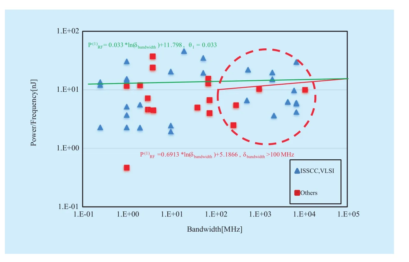
Fig. 3 RF statistical bandwidth-energy model
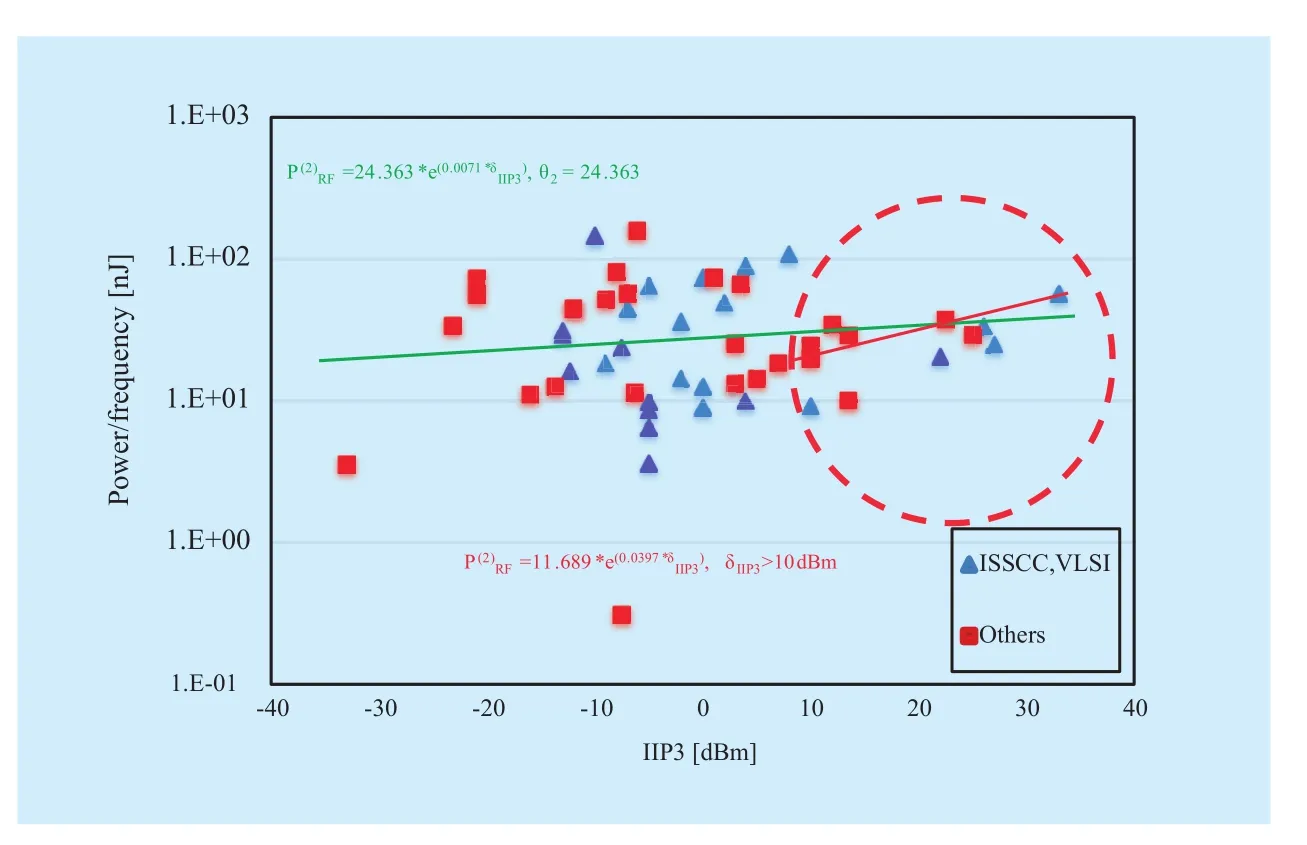
Fig. 4 Rx RF statistical IIP3-energy model
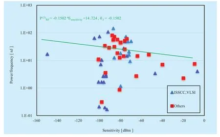
Fig. 5 Rx RF statistical sensitivity-energy model
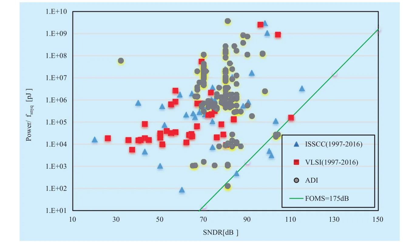
Fig. 6 DAC statistical power model
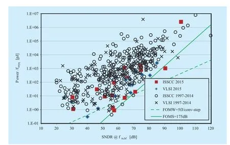
Fig. 7 ADC statistical power model
where,Poutis the output power radiated at antenna; σfrequency=0.02is the parasitic capacitance loss factor of CMOS and III-V semiconductors FET circuits (fcGHz); σpassive=0.15denotes passive component loss factor;σPPA=0.25(CMOS),σPPA=0.15(III-V semiconductors)is the power factor for pre-power amplifier whenfcis much less thanfmax.σPPAlargely depends on technology such as CMOS, Si Bipolar, GaN, GaAs, LDMOS[17]. σstructureis the circuit structure factor on PA efficiency including back-off [18]. σstruc-tureexposes the theoretical highest efficiency of the circuit for PA, for example, pulse width modulation ( σstructure=0.7), Doherty (σstructure=0.3~0.45) and others ( σstructure=0.1~0.2, e.g.,class A, class B). σfeedis a feeder loss of macro cell, due to the fact that base station sites and the antennas are often situated at different physical locations. In particular, this loss arises from antenna mismatch and the feeder cables. Feeder loss for smaller base stations can be negligible. It is to note that default figures provided are empirical values.
3.2.3 ADC/DAC
ADC/DAC is often overlooked due to its relatively small contribution for base station power consumption. Its power, especially the power of DAC, would play more significant roles in the upcoming 5G, when massive MIMO technique [19] is widely adopted. Consequently, in this paper, ADC/DAC power is modeled.
Similar to RF statistical model, we investigated the impact factors of DAC power dissipation (such as resolution, sampling rate,pin power, etc.) and collected available design cases, products from published papers and OEM (ADI). In Figure 6, distinguishable power distribution can be found (where fsnyq is Nyquist sampling rate, SNDR is signal to noise and distortion ratio); especially the distributed characteristic of ADI products is a useful guideline on product selection. On the other hand, 55mW DAC (I or Q, 12 bit precision, 500 MSPS, no decimation part and no pin cost) may be the best reachable entry point for 5G low power design. Likewise, in [16],the power distribution of ADC has been thoroughly analyzed, as illustrated in Figure 7. It can be seen that 100mW ADC (I or Q, 12 bit precision, 1000 MSPS and pin power) may be the best alternative for 5G.
There are two ways for ADC/DAC power estimation by using Fig.6 and Fig.7. First,designers can directly estimate the power consumption of new design according to target fsnyq and SNDR provided in two figures. Second, designers need to select the overall data or partial data in two figures to create regression models, and then the power consumption of target design can be predicted.
IV. OPTIMIZATION FOR MPSoC DESIGN
In Figure 1, each cluster in DBB MPSoC serves for one or more PHY modules (function) and contains one or more processing elements (hardware). Minimizing the power consumption of DBB MPSoC, according to(2), is equivalent to the minimization of the power consumed by each module. Meanwhile,two major factors impact on the power consumption of each module by (3), i.e., 1) the number of PEs within a cluster (degree of task parallelism) and 2) microarchitecture (all parameters in (3) exceptNtask_paralleldepending on microarchitecture). On the other hand,DBB as a hard real-time system must satisfy a runtime deadline specified by communication standard. Hence, in this section, based on the proposed DBB energy model, a power/energy optimization method under timing constraint is presented. This method selects a suitable microarchitecture and degree of task parallelism for each PHY module in digital baseband to minimize the power/energy consumption of the whole DBB MPSoC. Note that our optimization method mainly focuses on PE design without considering bus structure. Furthermore, this method is especially applicable to the design that more PHY modules than one are implemented in one processor.
Actually, selecting suitable microarchitecture for each PHY module, to minimize the whole baseband power dissipation, is a case of design space exploration (DSE) in system level design. However, when designing the PE microarchitecture for a module, there are two main differences between conventional DSE and energy/power optimization here.
1) Optimization goal: The goal of conventional DSE is to minimize the power consumption of a single module. By contrast, our target is to minimize the power consumption of the whole digital baseband.
2) Constraints: Timing constraint of conventional DSE is on module itself. In our optimization, the timing constraint is on the whole baseband (all modules).
In other words, for a same module, the suitable PE microarchitecture in our optimization is probably not the optimal one in conventional DSE, even though it (optimal one) contributes to power minimization of the whole digital baseband. Consequently, the traditional optimization algorithms (e.g., the greedy algorithm family: force directed scheduling,list scheduling… and the heuristic algorithm family: ant colony optimization, simulated annealing…[20] (chapter13)) used to explore the optimal operation scheduling may not be able to meet our demand. This is because both the greedy algorithm family and heuristic method family are likely to produce a sub-optimal solution due to the greedy nature and the dependence on probability. As a result, in this paper, a design space construction method and an optimization method based on this design space are proposed to explore the power/energy minimization MPSoC design of digital baseband.
4.1 Design space construction
Compared to traditional design space construction, our design space contains all of the potential PE microarchitectures (i.e., varied degree of data/task parallelism and pipeline)for each module. As illustrated in Figure 8,all of the candidate microarchitectures of the overall PHY modules need to be mapped to design space.
In fact, PE design space here is a weighted directed graphG =
Definition 1. In vertex setV,Vi,jϵVdenotes the candidate PE(s)jwith specific microarchitecture for the physical layer modulei. All of vertices of the moduleiare divided into different subsets by two basic indices: algorithm selection (red circle in Figure 8) and platform selection (green circle). Note thatV0just represents starting point.
A vertex in the PE design space may be a single PE or a group of PEs (a cluster, i.e.,task level parallel), as shown in the blue circle in Figure 8. Since only one vertex for each module can be selected in exploration process,multi-PEs within a cluster have to be gathered together as a single vertex. In particular, if there is no constraint on the number of PEs within a cluster, we can try to select different combinations of PEs. In addition, every vertex in the design space is already bound with an algorithm and a microarchitecture. If several PHY modules share a same cluster, e.g., Bit processor in Figure 1 support both CRC and Scrambling modules, then these modules should be separated as a sequence of a single module in terms of PE design exploration.Once the PE microarchitectures of these modules are determined using our optimization method, designers can further explore the maximum resource sharing of these microarchitectures for the shared cluster design.

Fig. 8 Design space exploration for MPSoC design
Definition 2. In directed graphG, there is always a directed edgeEij,(i+1)kϵEthat connectsVi,jandVi+1,k, and there is no edge betweenVi,jandVi,k. Meanwhile,Wij,(i+1)kϵWis the weight of edgeEij,(i+1)k, and its value is marked by end vertexVi+1,k(i.e., execution time).
4.2 Optimization method
Once PE microarchitecture design space is set up, graph algorithms can be selected to explore suitable option for each PHY module under timing constraints. A PE DSE for selecting suitable PE microarchitectures for all PHY modules is often a multistep decision-making process. In this paper, we thus choose shortest path algorithm (dynamic programming) as a default optimization method based on above design space.
Now letdG(u),dG(v)represent the shortest path from starting pointV0to vertexVuandVv,respectively, anddG(0)=0. Suppose thatTmax,WLpeakbe respectively timing constraint and peak workload of the whole PHY. Then, the goal of our optimization can be defined to be

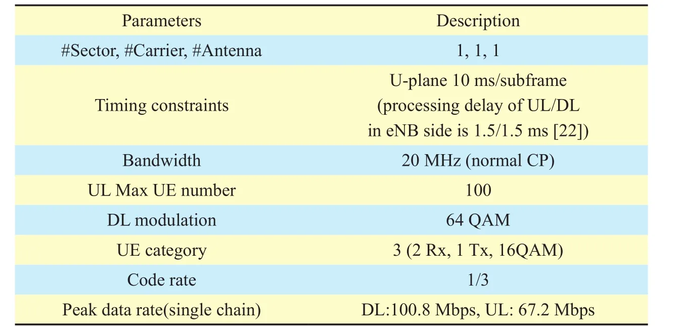
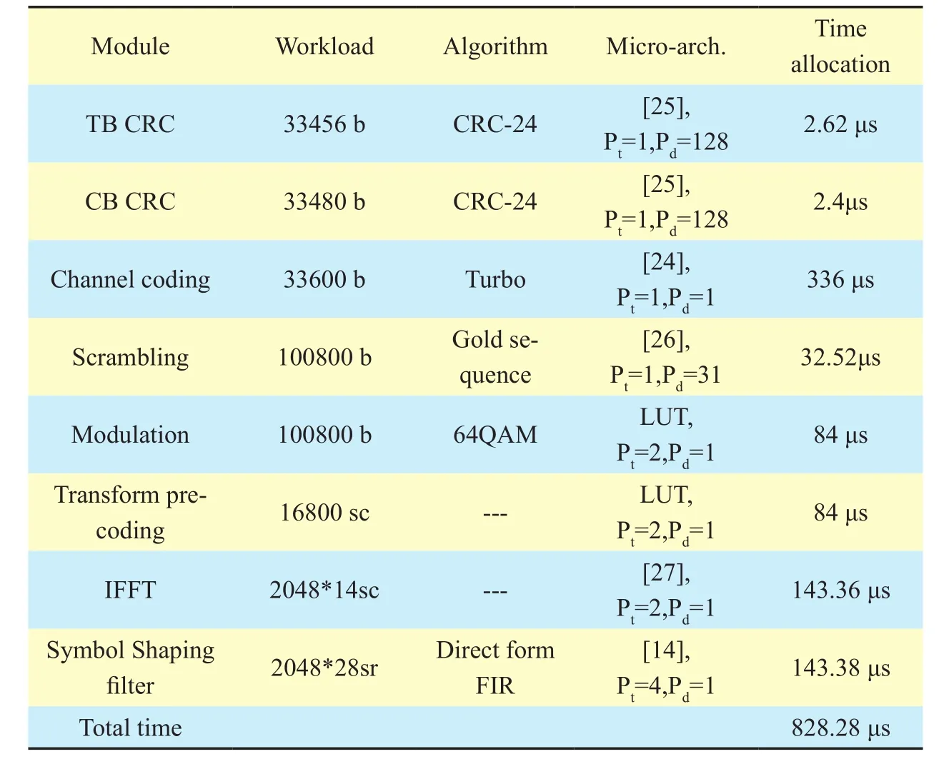
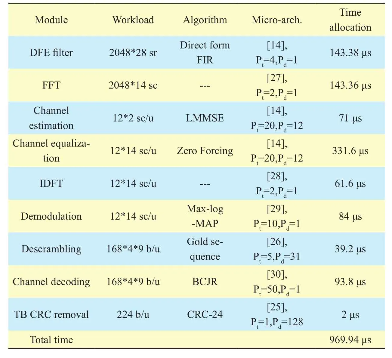
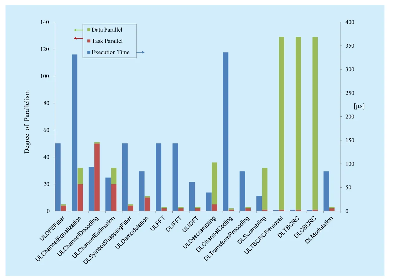
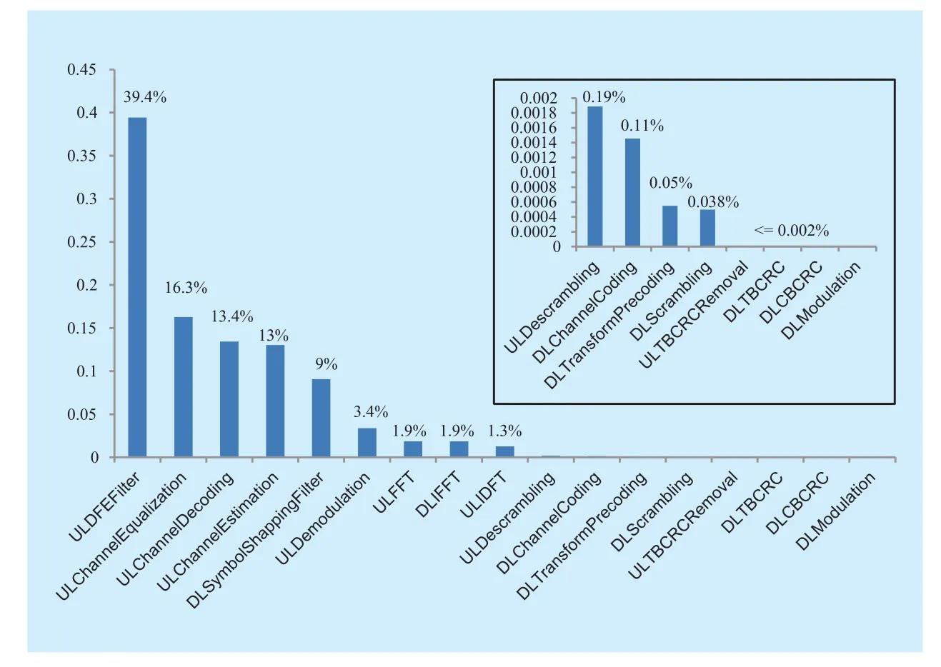
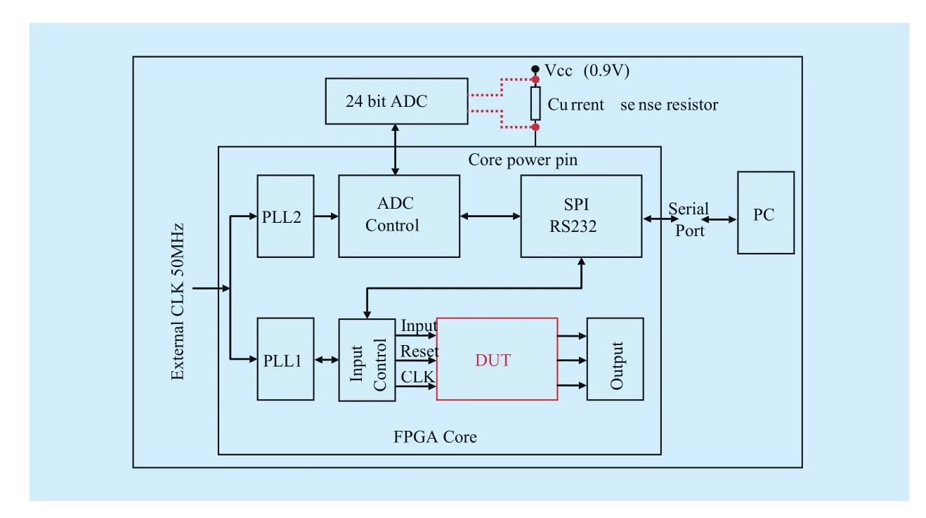
VertexVuis a subset of vertices of the moduleu, and only one vertex in this subset can be selected indG(u). By (10), the execution time of each vertexVi,jϵVin design space can be estimated withWLpeak, and is denoted byWij,(i+1)kϵW. For givenWij,(i+1)kϵW, we can apply shortest-path algorithms (e.g., Dijkstra,Bellman-Ford) on the weighted directed graph to execute global search and calculate optimal solutions. For optimal solutions, there exist two cases. On the one hand, if there is no solution, then designers need to add new candidate vertices to graphGand recalculate solutions.On the other hand, there exist one or more optimal solutions, in Figure 8, suppose bothd(1)G(n)=(V0, V11, V21, V31, V42…Vn1),d(2)G(n)=(V0,V13, V26, V32,V43…Vn2)meet timing constraintTmaxandd(1)G(n)= d(2)G(n)ord(1)G(n) Then, designers need to select the final solution for minimum power/energy consumption (optimization) from the collection of optimal solutions. Based on the tradeoff between execution time and power consumption, the optimal solution of shortest path is the minimum execution time of all PHY modules,but power consumption is probably the max.Actually, the Pareto optimal path of our power optimization problem probably is the longest path which satisfies the timing constraintTmax,e.g., from the second case, the Pareto path isConsequently,designers have to calculate the power consumption of each vertex in pathd(1)G(n), d(2)G(n)by using (3) and compare their power values. Smaller one is the Pareto optimal path for power optimization of the whole DBB MPSoC. Meanwhile, microarchitecture and degree of task parallelism of each PHY module are determined by corresponding vertex in Pareto optimal path (e.g.,d(2)G(n)). Likewise,energy consumption for pathd(1)G(n), d(2)G(n)can be further calculated to identify the Pareto optimal solution for energy minimization. Finally, a Pareto optimal MPSoC DBB design with minimum energy/power can be identified. Meanwhile, the goal of microarchitecture selection and degree of task parallelism determination for each PHY module can be achieved as well. This optimization method has been applied to our digital baseband design introduced in section 5.1. Actually, towards different optimization goals, designers can select distinct constraints (timing, power, area, and throughput)as weightsW. DBB and PA are currently two major power greedy subsystems in typical base stations [3][21]. In this section, as an example, a reference design for digital baseband MPSoC under timing constraints is introduced to expose the details about DBB energy consumption.PA power consumption is also estimated and compared with measured results in [3]. 5.1.1 Scenario assumptions and time allocation As a kind of hard real-time embedded system,digital baseband subsystem in base station must satisfy the time constraints specified by communication standard at maximum load.For instance, even though there are 6 supported bandwidths (1.4MHz~20MHz) available in LTE, DBB designers have to follow corner conditions, i.e., 20MHz. Consequently, extreme scenario for our reference design is listed in Table I. Under the scenario, time allocation for each PHY module in UL/DL [23][24] is conducted under UL/DL timing constraint, i.e., 1.5/1.5 ms. Time allocation in our reference design focuses on PHY and part of MAC. We took 1 ms/subframe as practical timing constraint for time allocation of major PHY modules in UL/DL. Extra 0.5 ms is used for data processing of PDCP (packet data convergence protocol),RLC (radio link control), MAC (medium access control) and other PHY modules in DL/UL, e.g., resource element mapping in DL,and burst detection in UL. Note that our reference design mainly focuses on PE design of MPSoC without considering bus structure(Figure 1). Time allocation process can be simply stated as follows (suppose the algorithm set and the microarchitecture set for each PHY mod-ule are already constituted; for simplicity, the assumption of block processing is made; clock frequency is 100 MHz; 16 bit×16bit multiplier need 1 clock cycle): Table I LTE scenario assumptions for DBB reference design (LTE FDD macro cell) Step 1– Initial allocation: Initially, time constraint of the whole UL or DL PHY (1000 μs) is equally divided into 8 or 9 parts according to the number of DL PHY modules or UL PHY modules. Therefore, each module has an identical time slot, i.e., 1000/8=125μs (DL) or 1000/9=111.11μs (UL). Step 2– Algorithm and microarchitecture selection: Algorithm and microarchitecture of each module are selected to satisfy the allocated time constraint under the workload for 20MHz bandwidth. When selecting microarchitecture and algorithm for each module, the execution time models proposed in 3.1 are utilized to estimate the execution time for each microarchitecture. For instance, suppose there are two alternatives in DL TBCRC microarchitecture set, i.e., LFSR and 128-way data parallel CRC architecture [25], then LFSR needs about 33456 cycles (334.56μs) and the other needs 262 cycles (2.62μs) to compute 33456bit data. Thus, the latter is chosen as the candidate microarchitecture for TBCRC module,to follow the requirements 334.56μs>125μs and 2.62μs<125μs. In our reference design,algorithm and microarchitecture are selected by using the optimization method presented in section IV. Table II Time allocation for DL PHY modules in eNB (TB: transfer block, CB:code block, b: bit, sc: symbol with complex data and 16bits precision, sr: symbol with real number data and 16bits precision, ---: no limit, Pt: degree of task parallelism, Pd: degree of data parallelism) Step 3– Parallelization: Generally, for increasing the throughput of an original module without task level parallelization, data parallelization will be applied first. Like the TBCRC example shown, LFSR as an original microarchitecture computes one input bit at a time and the other parallel structure computes 128 bit in parallel. Hence, the microarchitecture set of a module is often with the varied degree of data parallelism. However, if data parallelization is unavailable, then we have to increase task level parallel to reduce execution time. Task parallel is like a “duplicate” operation that clones a copy of an existing module,leading to two or more modules running in parallel. Thus, the power consumption increases along with increment of task level parallel.As previously mentioned in section IV, under timing constraints, both microarchitecture selection and task parallelization of each PHY module aim at minimizing the energy/power consumption of the whole baseband. It is a NP-hard optimization problem. By using above optimization method, suitable microarchitecture and degree of task parallelism of each PHY module are determined and listed in Table II, III. Meanwhile, time allocation of our reference design is fulfilled as well, shown in Figure 9 and column ‘Time allocation’ in Table II, III. In Table II, LUT is lookup table for modulation and precoding respectively, and the table stores complex number and codebook specified in [23]; symbol shaping filter is a 26-taps FIR filter. In Table III, DFE is simplified as a 112-taps FIR equivalent to all functions including decimator, rotator, farrow filter and channel filter; matrix inversion of LMMSE is QR decomposition based on Gram-Schmidt; in terms of channel decoding module, a task is a single SISO turbo decoder with 10 decoding iterations; the data precision of LLR (soft bits) is 9 bit. 5.1.2 System level power estimation and analysis Once microarchitecture and task parallel for each PHY module is determined, the logic gates, macro blocks (multipliers, adders and registers) and memory access operations inside a microarchitecture can be precisely counted. For DSP and ASIC platforms, power consumption of each module can be directly estimated by using the power model with specified standard cell library of a CMOS IC technology. Whereas, for FPGA platform, it is usually hard to obtain the accurate logic elements count without the help of synthesize tool. Thus, this paper offers a fast and near accurate power estimation method for FPGA platform, before logic synthesis, based on reuse block at system level as follows. First, all of basic components (e.g., adder)used in microarchitecture of all PHY modules are collected. The power consumption of each basic component is measured. In our reference design, the power consumption of 32bit full adder, 16bit multiplier, 16bit D Flip-flop,XOR gate, digital comparator and memory operation is measured on specified FPGA and normalized by the multiplier power. Power consumption of other basic components is negligible. FPGA technology weighting factor is measured, for example, a 16bit×16bit multiplier is 0.0303 mW at 100 MHz in AlteraTMStratix IV GX FPGA. Normalization power consumption arePmul=1/MHz,Padd= 0.6/MHz,Pxor= 0.012/MHz,Pdff= 0.027/MHz,Pcomparator= 0.02 /MHz,Pmemory_access=0.33/Kbit /MHz. Next, with normalized components power and the optimization results of microarchitecture selection with specified task parallel,relative power estimation of all PHY modules can be achieved using our power model (3),as illustrated in Figure 10. In Figure 9, the higher task parallel and data parallel is, the less execution time is. Meanwhile, the power dissipation of corresponding module in Figure10 gets higher. On the other hand, power consumption greatly depends on algorithm complexity as well. For instance, even though the execution time of channel equalization module is not yet minimized, its power consumption is sufficiently high due to high complexity of Gram-Schmidt algorithm. Hence, if designers intend to further minimize the execution time of this module without increasing power,Gram-Schmidt has to be replaced by low complexity algorithm. . Table III Time allocation for UL PHY modules in eNB (DFE: digital front-end,LMMSE: linear minimum mean square error, MAP: maximum a posteriori, sc/u:symbol/user, b/s: bit/user) Fig. 9 Time allocation with specific data and task parallel Fig. 10 Proportional distribution of relative power estimation Fig. 11 Test bench based on DE4 power measurement Finally, one or more modules (reuse blocks)are selected to perform the absolute power calibration (to be discussed in section 5.1.3),and power estimation of the rest modules (new design blocks) can be directly derived from the power calibration of reuse blocks and the relative power ratio in Figure 10. 5.1.3 Experiment setup and power calibration To illustrate the calibration method, AlteraTMDE4 (2010 products) development board with Stratix IV GX FPGA is chosen to measure and evaluate the power consumption of selected modules. There are 12 power supply rails with on-board voltage and current sense capabilities. Built-in 24-bit ADC devices and provided voltage/current measurement methods are used. A power test bench is set up, shown in Figure 11. Downloading the netlist into FPGA core, i.e., device under test (DUT), and feeding random stimuli patterns (data switching activity is 0.5) to DUT via ‘input’ port. The differences (keeping the same FPGA mapping and layout for calibrations with/without DUT)of the electric current on sense resistor of the power supply rail are collected by ADC and transferred to PC. Note that the power measurement of DUT does not contain the power of pins, global wire, main memory and other peripherals on board. Once the power figures of selected modules are obtained, the power dissipation of all modules in the reference design can be indirectly figured out according to the ratio of power consumption exposed in figure 10. In this paper, channel decoding module is measured. Actually, a 12 soft-input soft-output (SISO)decoder in parallel was used for measuringpower dissipation. To reduce measurement error, the power data collection comprised 100 test groups and each test group contained 10 samples. Each test group was marked with the average of 10 samples. Finally, the mean value of 100 test groups was the final measured power of the channel decoding module.Additionally, there were two cases in each test group: Table IV Comparison of PA power estimation (σfeed: feeder loss, ηeffi ciency: PA efficiency, PPA: PA power consumption. The carrier frequency=2.1 GHz is assumed in [3], and other parameters (σfrequency, σpassive, σPPA) in (13) are default values.) 1) After ‘Reset’ DUT, ‘Input’ and ‘CLK’ports are enabled, and thus the dynamic power combined with static power is measured; 2) After ‘Reset’, disabling the ‘Input’ port and ‘CLK’ port and thus static power of the FPGA core is measured. Hence, the dynamic power of DUT can be computed by means of the whole power measured in 1) subtracts the static power in 2). The power measurement of 1) and 2) was respectively sampled 10 times for each test group. Through sufficient measurements, the power consumption of 12 parallel SISOs at 100MHz was 1.02W. The power of 50 SISOs was figured out by scaling it up, i.e., 4.25W.Finally, the dynamic power consumption of all PHY modules in our reference design was 4.25/0.134=31.7 W (the relative power proportion of the channel decoding module is 13.4%in Figure 10). The main problems when comparing our power estimation with measured DBB power in other literatures are: the difference lie in 1) algorithm selection, 2) microarchitecture selection and 3) platform selection. However, there is still similarity in communication standard and extreme conditions. In [3], even though the processors solution for DBB is used for power measurement (in 2010), there is a slight difference between their dynamic power 29.6 W (macro cell) and our estimation 31.7 W. This is mainly because both designs are for LTE standard under the same extreme conditions, i.e., peak traffic load. Moreover,we selected FPGA product (Stratix IV GX of 2010) in measurement to further match silicon technologies in 2010. Actually, with the increasing of reuse blocks in new design,more and more low-level physical information can be obtained in early system design stages.Therefore, more accurate power/energy estimation can be achieved. Table IV shows the comparison results for PA power estimation of various LTE base station types by using our model (13) and PA power model presented in [3]. The purpose is to validate our PA power model. --Macro cell and RRH (remote radio head): Since the digital pre-distortion and Doherty structure are both taken into account for macro cell and RRH in [3], the power efficiency is improved. Thus σstructure=0.45(Doherty structure) in our PA model (13) is chosen to estimate power consumption of macro cell and RRH. As shown in Table IV,our power estimations of them are slightly higher than the measured values in [3], i.e.,132.8>128.2 and 66.6>64.4, which arises from the digital pre-distortion. Power estimation errors are (132.8-128.2)/132.8=3.5% (macro),(66.6-64.4)/66.6= 3.3% (RRH), respectively. --Micro cell: Though the digital pre-distortion and Doherty structure are also used for micro cell [3], uncertainty factors result in obvious PA efficiency reduction by comparison with RRH, i.e., 22.8%<31.1%. Then, σstruc-ture=0.45 may be not appropriate in terms of a(27.7-21)/27.7=24% power estimation error. --Pico cell and Femto cell: In [3], the high operating back-off gives rise to poor power efficiency in smaller base station types due to the lack of advanced structures and digital pre-distortion support. Thus σstructure=0.1 in our PA model is a suitable choice for power estimation of pico/femto base stations. Power estimation errors are (1.95-1.9)/1.95=2.6%(pico) and (1.1-0.75)/1.1=31.8% (femto), respectively. The other information involved in our PA model is not exposed in [3], e.g., passive component loss factor, otherwise, we can further fine-tune other parameters in the PA model.The power estimation error will be further reduced. (More PA details can be found in [18]) Even though 5G is not yet standardized, some key technologies have been released in [31][32][33]. Then some design explorations should and can be conducted, e.g., building algorithm/microarchitecture sets, finding the entry point of low power design, making a power budget of pre-designed base stations, etc.Obviously, such explorations can benefit from our models. We will introduce and discuss reference system designs for 5G scenarios in our future work. In this paper, a holistic power/energy estimation model is proposed for base station system early-stage design. Even without sufficient physical information, fast and near accurate power/energy estimation can be achieved at system level by using this model. This model opens up more opportunities, comparing to existing models, for system designers and users to explore their energy-efficient technologies for 4G and early-stage designs of the future base stations. Additionally, an energy/power optimization method based on our DBB energy model is proposed. By this optimization method, designers can rapidly evaluate distinct DBB design alternatives and find optimal DBB designs for energy minimization. A software platform based on the proposed models and optimization methods has been developed. We will find more application scenarios for energy saving during designs and operations. The finance supporting from National High Technical Research and Development Program of China (863 program) 2014AA01A705 is sincerely acknowledged by authors. 1. The main abbreviations of the paper are listed here. [1] 3GPP TR 36.927,“Potential Solutions for Energy Saving for E-UTRAN”, 2012,www.3gpp.org/dynareport/36927.htm [2] J.G Andrews, S. Buzzi, W. Choi,et al, “What Will 5G Be?”.IEEE Journal on Selected Areas in Communications, vol.32, no.6, pp 1065–1082, June,2014. [3] G. Auer, V. Giannini, C. Desset,et al, “How Much Energy Is Needed to Run a Wireless Network”,IEEE Wireless Communications, vol. 18, no. 4, pp 40-49, Oct. 2011. [4] O. Arnold, F. Richter, G. Fettweis,et al, “Power Consumption Modeling of Different Base Station Types in Heterogeneous Cellular Networks”,IEEE 2010 Future Network & Mobile Summit. Florence, June, 2010, pp 1–8. [5] C. Desset, B. Debaillie, V. Giannini,et al, “Flexible Power Modeling of LTE Base Stations”,IEEE Wireless Communications and Networking Conference (WCNC), Apr. 2012, pp 2858–2862. [6] R.V.R Kumar, J. Gurugubelli, “How Green the LTE Technology Can Be?”,IEEE 2011 2nd International Conference on Wireless Communication,Vehicular Technology, Information Theory and Aerospace and Electronic Systems Technology,Mar. 2011, pp 1-5. [7] H. Holtkamp, G. Auer,et al, “A Parameterized Base Station Power Model”,IEEE Communications Letters, vol.17, no.11,pp 2033–2035, Nov.2013. [8] H.K Boyapati, R.V Rajakumar, S. Chakrabarti,“Quantifying the Improvement in Energy Savings for LTE eNodeB Baseband Subsystem with Technology Scaling and Multi-core Architectures”,IEEE 2012 National Conference on Communications (NCC),Feb. 2012, pp 1-5. [9] H.K Boyapati, R.V.R Kumar, S. Chakrabarti,“Characterization of Baseband Implementations Using Energy Efficiency Metric Based Quantification”,IEEE 2011 International Conference on Devices and Communications (ICDeCom), Feb.2011, pp 1-5. [10] K. Keutzer, A.R Newton, J.M Rabaey, et al,“System-Level Design: Orthogonalization of Concerns and Platform-based Design”,IEEE Transactions on Computer-Aided Design of Integrated Circuits and Systems,vol.19, no.12, pp 1523–1543, Dec. 2000. [11] W. Wang, X.Y Li, D. Liu,et al, “Multilevel Power Modeling of Base Station and Its ICs”,China Communications, vol. 12, no.5, pp 22–33, May,2015. [12] “International Technology Roadmap for Semiconductors (2007), Design”, 2007, http://www.itrs2.net/itrs-reports.html [13] N.A Sherwani, “Algorithm for VLSI Physical Design Automation”,Dordrecht, NED. Kluwer Academic Publishers, 2002. [14] D. Liu, “Baseband ASIP Design for SDR”,China Communications, vol.12, no.7, pp 60–72, July,2015. [15] “International Technology Roadmap for Semiconductors (2013), Interconnect”, 2013, http://www.itrs2.net/itrs-reports.html [16] B. Murmann, “ADC Performance Survey 1997-2016”, http://web.stanford.edu/~murmann/adcsurvey.html [17] H.S Bennett, R. Brederlow, J.C Costa,et al, “Device and Technology Evolution for Si-based RF Integrated Circuits”,IEEE Transactions on Electron Devices, vol.52, no.7, pp 1235–1258, July,2005. [18] S.C Cripps, “RF Power Amplifiers for Wireless Communications”,Norwood, MA,USA. ARTECH HOUSE, 2006. [19] F. Boccardi, R. Heath, A. Lozano,et al, “Five Disruptive Technology Directions for 5G”,IEEE Communications Magazine, vol. 52, no. 2, pp 74–80, Feb. 2014. [20] P. Coussy, A. Morawiec, “High-Level Synthesis From Algorithm to Digital Circuit”,Springer,2008. [21] B. Debaillie, A.Giry, M.J Gonzalez,et al, “Opportunities for Energy Savings in Pico/Femti-cell Base-Station”,IEEE Future Network & Mobile Summit 2011 (FutureNetw), June, 2011, pp 1–8. [22] Telecommunications Industry Association, “TR-45 Ad-Hoc Group on International Mobile Telecommunications, TR-45 -AHIMT (2008)”,ftp.tiaonline.org/TR-45/TR-45_AHIMT/Public/TR-45_Final_Report.pdf [23] 3GPP TS 36.211, “Evolved Universal Terrestrial Radio Access (E-UTRA):Physical channels and modulation”, 2010, http://www.3gpp.org/ftp/Specs/archive/36_series/ [24] 3GPP TS 36.212, “Evolved Universal Terrestrial Radio Access (E-UTRA):Multiplexing and channel coding”, 2010, http://www.3gpp.org/ftp/Specs/archive/36_series/ [25] Y.H Huo, X.Y Li,W. Wang,et al, “High Performance Table-Based Architecture for Parallel CRC Calculation”,The 21st IEEE International Workshop on Local and Metropolitan Area Networks, Apr. 2015, pp 1–6. [26] Y.T Hwang, J.Y Chen, M.H Sheu, “Automatic Generation of Programmable Parallel CRC &Scrambler Designs”,2006 IEEE Workshop on Signal Processing Systems Design and Implementation (SIPS), Oct. 2006, pp 286–291. [27] C. Yu, M.H Yen, “Area-Efficient 128- to 2048/1536-Point Pipeline FFT Processor for LTE and Mobile WiMAX Systems”,IEEE Transactions on Very Large Scale Integration (VLSI) Systems,vol. 23, no. 9, pp 1793–1800, Sep. 2015. [28] Ji.N Chen, J.H Hu,et al, “Hardware Efficient Mixed Radix-25/16/9 FFT for LTE Systems”,IEEE Transactions on Very Large Scale Integration(VLSI) Systems,vol. 23, no. 2, pp 221–229, Feb.2015. [29] A. Gomaa, L.M.A Jalloul, M. Mansour, “Max-Log-MAP Optimal MU-MIMO Receiver for Joint Data Detection and Interferer Modulation Classification”,IEEE Communications Letters, vol. 20,no. 7, pp 1389–1392, July, 2016. [30] Z.Z Wu, D. Liu, “High-Throughput Trellis Processor for Multistandard FEC Decoding”,IEEE Transactions on Very Large Scale Integration(VLSI) Systems, vol. 23, no. 12, pp 2757–2767,Dec. 2015. [31] IMT-2020 (5G) Promote Group, “White Paper on 5G Wireless Technology Architecture”, 2015. [32] P. Z Fan, J. Zhao,et al. “5G High Mobility Wireless Communications: Challenges and Solutions”, [J]China Communications, Vol. 13, no.Supplement2, pp: 1-13, Jan. 2017. [33] X. Meng, J. Li,et al. “5G Technology Requirements and Related Test Environments for Evaluation”, [J]China Communications, Vol. 13, no.Supplement2, pp: 42-51, Jan. 2017.V. A CASE STUDY
5.1 Digital Baseband

5.2 Power amplifier
VI. CONCLUSION
ACKNOWLEDGEMENTS
Note

- China Communications的其它文章
- Efficient Subchannel Allocation Based on Clustered Interference Alignment in Ultra-Dense Femtocell Networks
- X-Band Power Amplifier for Next Generation Networks Based on MESFET
- A VMIMO-Based Cooperative Routing Algorithm for Maximizing Network Lifetime
- Efficient Packet Scheduling Technique for Data Merging in Wireless Sensor Networks
- A Novel Forwarding Method for Full-Duplex Two-Way Relay Networks
- Versatile Routing and Self-Certifying Features Support for Secure Mobility in eXpressive Internet Architecture

