A Three-Dimensional Surface Miacromachining Process Simulation System Based on the Narrow Band Level Set Method*
LI Ning,ZHOU Zaifa,HUANG Qingan,YU Jiacheng(Key Labortory of MEMS of the Minisry of Education,Southeast University,Nanjing 210096,China)
A Three-Dimensional Surface Miacromachining Process Simulation System Based on the Narrow Band Level Set Method*
LI Ning,ZHOU Zaifa*,HUANG Qingan,YU Jiacheng
(Key Labortory of MEMS of the Minisry of Education,Southeast University,Nanjing 210096,China)
The surface micromachining process is a main manufacturing method for Micro-Electro-Mechanical-System(MEMS). A new system for three-dimensional(3-D)simulation for this process with multi-layer is presented. The surface evolution algorithm is based on the narrow band level set method,because it is stable and computation efficient and also can easily handle the topographic changes to certificate the accuracy of the simulation system. A serious of simulations have been designed and performed using this simulation system. Compared with the scanning electron microscopy(SEM)pictures,the simulation results of the micro-rotating structures were demonstrated to be accurate,efficient. The system provides cost-effective,proof-of-concept for the MEMS devices manufacture,reducing the design cycle.
MEMS;simulation system;surface micromachining process;narrow band level set method
The surface micromachining process has a good compatibility with the CMOS technology,and at the same time it is also one of the most common and commercialized processing techniques,and one core technology for the super-large-scale integration. It can take advantage of the deposition order of different materials on the silicon wafer,and then chooses the appropriate etching ways to make various kinds of micro structures[1]. Until now almost all the MEMS devices have the units processed by this process,and the multi-gear transmission made by the American SANDIA laboratory,is an example of a typical planar process used in micromachining systems. A simulation system for this process has a great significance for the real MEMS device fabrication.
Since the traditional simulation is complex,time consuming,and hard to change the parameters. To solve the above problems,we have to improve the algorithm of the profile evolution and add a system interface. The Monte Carlo simulation method was used to determine the profile evolution according to the substrate surface interaction[2]. The model is more accurate,but it is time consuming. The model in reference[3] just considered the influence of reactant transport on the reactive ion etching(RIE),but it neglected the deposition process.
In this article,the numerical modeland[4]the narrow band level set method[5-6]are utilized to develop the simulation system for the surface micromachining process,aiming to reduce simulation time and decrease the cost. And the system is demonstrated to be efficient and accurate. The system provides:parameters control module,including the time,rate,geometric parameters of the mask,that could be changed according to different processes;The mask loading module,loading the CIF file exported from the L-Edit v8.30;The expansion module,loading the Exposure software to visualize the simulation results. The developers could base on the simulation results to modify the model and algorithm. This system shorts the development cycle.
1 Model of the Surface MicromachingProcess
The micro-rotating structures which were fabricated using the standard surface micromachining process were used as an example in this paper. The process of this structure begins with(100)silicon wafers. Firstly,a 600 nm low-stress low pressure chemical vapor deposition(LPCVD)silicon nitride layer is deposited on the wafer as an electrical isolation layer,which is followed directly by the deposition of a 500 nm LPCVD polysilicon film Poly-0. Poly-0 is then patterned by photolithography and etched in plasma. A 2μm thick deposited oxide(PSG)sacrificial layer is deposited by LPCVD,annealed at 1 050 ℃ in argon and then patterned,followed by the deposition of a 2 μm thick polysilicon layer Poly-1. After Poly-1 is etched by RIE techniques,a second sacrificial PSG layer is deposited,annealed and patterned at a thickness of 750 nm. The third polysilicon film,Poly-2,is then deposited by LPCVD. Both Poly-1 and Poly-2 are doped with phosphorus from the PSG layers during the annealing process. The final deposited layer is a 0.5 μm metal layer that provides for probing,bonding,electrical routing and highly reflective mirror surfaces. The metal can be deposited and patterned by the lift-off process. Finally,the PSG layer is etched by RIE,and frees the microstructures[7]. In this study,Poly-1 is the structural layer,and the first sacrificial layer provides the gap under the structure. The piezoresistive cantilever beam in reference[8] was fabricated use this process.
1.1 RIE model
For the RIE process,the physical action and chemical action are concomitant. According to the characteristic of the reactive atoms,when the plasma enters into the substrate,the reaction could be illustrated by the schematic diagram as shown in Fig.1.
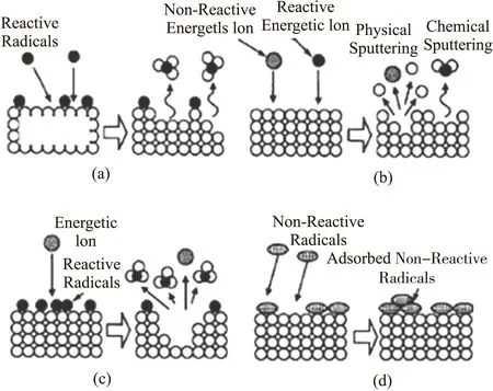
Fig.1 RIE schematic diagram
The RIE is a complex physical and chemical process,where there are many parameters can be regulated,like the atmospheric pressure,temperature. In this paper,the substrate is silicon,the fluorine-contained(CF4,SF6)was chosen as the etching plasma to etch the substrate with the isotropic manner. The CF4 and the SF6 were decomposed into CFx,SFx,andF,which could react with the silicon to produce the SiF4,that is violated. Meanwhile by increasing 10% oxygen could make etching rate increase 10 times,and set the etching temperatureT=400 K,the reaction chamber pressureP=20 mTorr,and the discharge power equals to 300 W.
The mechanism of etching model in the process could be viewed as the etching model described in reference[4]. The etching rate could be divided into two parts:a uniform etching and an ion-assistant etching.
ER=ERuni+ERion
(1)
The ERunican be viewed as a constant. The ion-assistant etching rate is expressed as following:
(2)
Where ERionis the ion-assistant etching rate,Cionis a constant,n and i are the unit vectors of the surface normal direction and ion incident direction,respec-tively,and α is the angle between the distribution function of ion flux.
(3)
Whereσis the standard deviation,Ωis the visible solid angle.
1.2 LPCVD model
LPCVD is deposited under the plasma at low pressure,which could make the thin film to be more perfect. The silicon dioxide deposition process from tetraethyleneoxysilane(TEOS)is deposited at the temperature of 1 023 K and 1.3 Torr.
The deposition model is also the combination of the isotropy and anisotropy.
DR=DRiso+DRani
(4)
The isotropic reaction is the main factor of influence and could be simplified as a constant.
DRiso=Ru
(5)
While the anisotropy rate,considering the effect of the contributions of the incoming particles,can be given by reference[8].
(6)
WhereRdis the deposition rate on a flat wafer without shadowing,Fd(Ω)is the angular distribution function of the incoming particles,which is cosine-based flux distribution function,as described in reference[9].
Fd(Ω)=cosn(AΘ)/NΘ≦π/2A
(7a)
Fd(Ω)=0 otherwise
(7b)
WhereArestricts the angle of incoming particles,n is used to describe over-cosine and under-cosine distributions,Nis a normalization factor.
1.3 Narrow band level set method
The level set method needs to compute the evolution of all the level sets,not only the zero level set. While the narrow band level set method,performing work just in the neighborhood of the zero level set. Under this circumstance,the operation in 3-D forN3grids points is reduced to beO(kN2),where k is the number of cells in the narrow band. The basic idea of the method is to tag grid points as“alive”,“land mine”,or“far away”,relying on whether they are inside the band,near its boundary,or outside the band,respectively. In Fig.2,the black disks are“alive”,the black disks on the edge of the band are“narrow band”points,and the open circles correspond to the“far away”points. Just store the points in the band,instead of storing the full 3-D grid of the points.

Fig.2 The mechanism of the narrow band level set method
Thus,just considering the computation on the alive points,and the band should be reconstructed when land mine points are reached. This reconstruction,known as“re-initialization”,is simply recalculated as fast as discussed in reference[10-11]. Typically,this narrow band method is faster than the full band level set method,cutting the time and lifting efficiency.
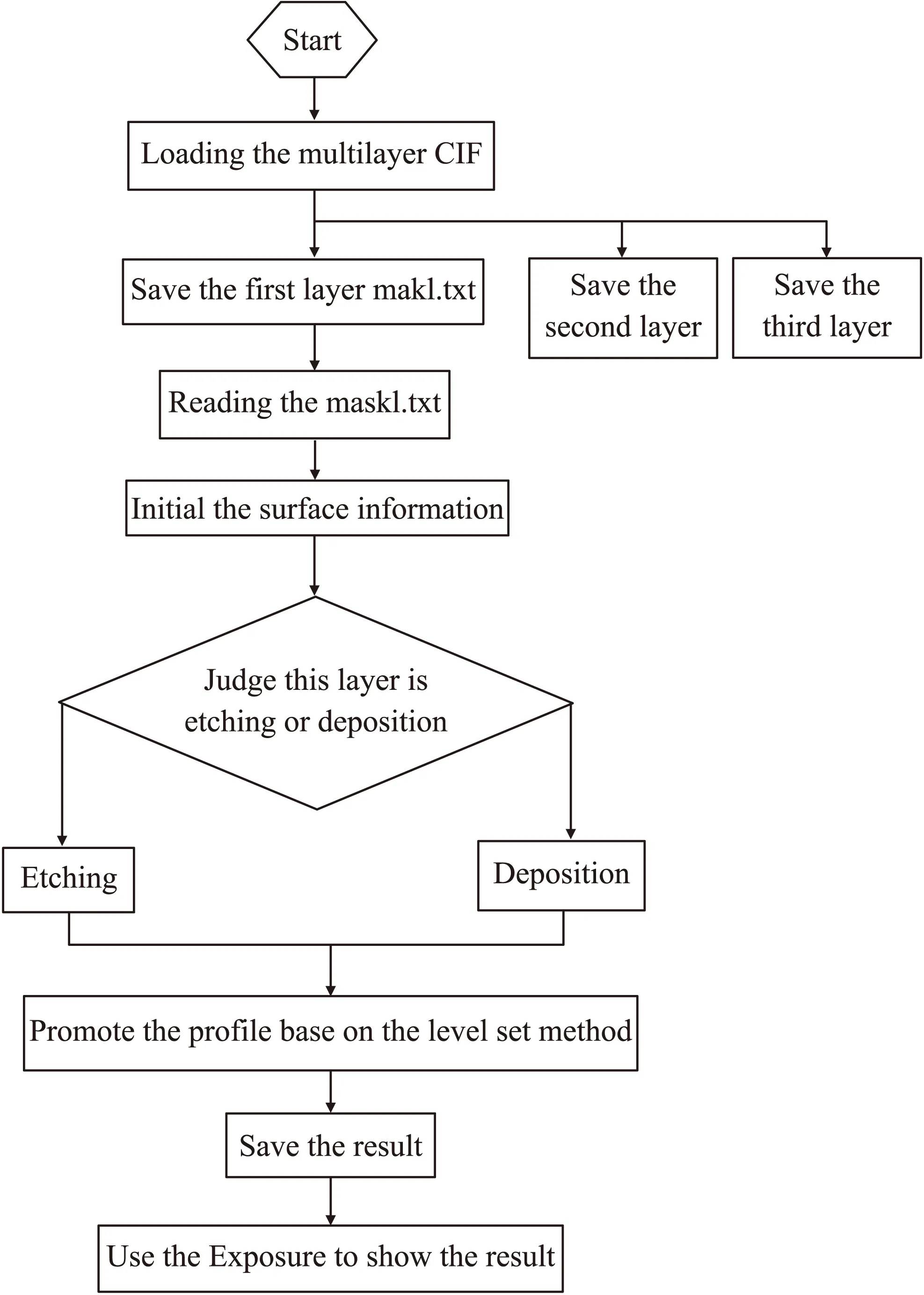
Fig.3 The software flow chart
2 Results and Discussion
The flow chart of the simulator is demonstrated as Fig.3. Because the flow charts of second layer and the third layer are the same as first layer,they were neglected in this figure.
2.1 Thin surface micromachining simulation system
In this paper,there are two micro-rotating structures for parameters extraction[12]simulated,the first structure is shown in Fig.4,the geometric structure is as following:L1=300 μm,W1=12 μm,L2=100 μm,W2=5 μm,L3=20 μm,W3=20 μm,L4=50 μm,W4=50 μm,L5=90 μm.

Fig.4 The schematic view of the first micro-rotating structure
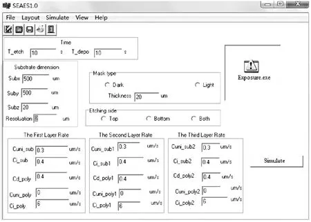
Fig.5 The interface of the simulator
2.2 Simulation results and discussion
To verify the simulator,some simulations have been implanted. Fig.5 is the interface of the simulator. Fig.6 shows the etching/deposition time and other parameters for the simulation. The simulation process for individual steps is shown in Fig.7. Fig.7(a)is the(100)silicon wafer and Fig.7(b)shows the result after the nitride deposition. Fig.7(c)is the result after the Poly-0 patterned and etched. Fig.7(d)and Fig.7(e)are the results after Poly-1,Poly-2 patterned and etched,respectively.The comparison between the experimental and simulation results were shown in Fig.8. Fig.8(a)is the CIF file,Fig.8(b)is the simulation result,and Fig.8(c)is the SEM photograph. The simulation time is about 20 minutes on a Pentium Ⅳ machine and the memory usage is about 20 Mbyte.

Fig.6 The simulation settings after loading CIF file

Fig.7 The first structure simulation process

Fig.8 The first experiment result
Like the first structure,the second structure is shown in Fig.9,the geometric structure is as following:L1=360 μm,W1=10 μm,L2=360 μm,W2=10 μm,L3=6 μm,W3=4 μm,L4=4 μm,W4=4 μm,L5=6 μm,L6=5 μm.
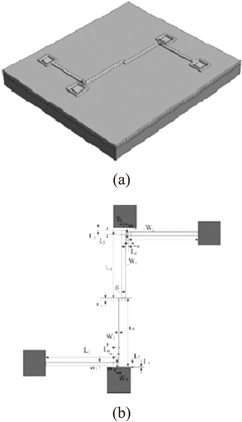
Fig.9 The schematic view of the second micro-rotating structure
The simulation process and the environmental settings are like the first structure. Fig.10 is the simulation of the second structure. Fig.10(a)is the(100)silicon wafer and Fig.10(b)shows the result after the nitride deposition. Fig.10(c)is the result after the Poly-0 patterned and etched. Fig.10(d)and Fig.10(e)are the results after Poly-1,Poly-2 patterned and etched,respectively.
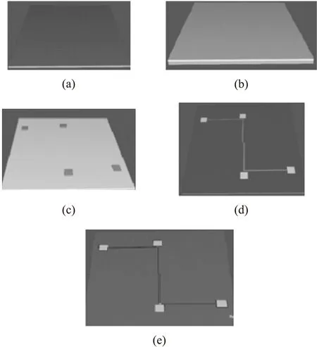
Fig.10 The second structure simulation process
Fig.11 is the comparison between the experi-mental and simulation results. Fig.11(a)is the CIF file,Fig.11(b)is the simulation result,and Fig.11(c)is the SEM photograph.
3 Conclusions
This paper presents the surface micromachining process simulation system based on the narrow band level set method. The comparisons between the simulation results and the SEM photographs verify the system to be efficient and stable. In further study we will focus on the physical model to improve the performance of the simulation system.
[1] Hsu T R. MEMS and Microsystes:Design and Manufacture[J]. Boston:McGraw-Hill,2002:49-50.
[2] Marcos G,Rhallabi A,Ranson P. Monte Carlo Simulation Method for Etching of Deep Trenches in Si by a SF6/O2 Plasma Mixture[J]. J Vac Sci Technol A,2003,21:87-95.
[3] Arnoid J C,Gray D C,Sawin H H. Inflence of Reactant on Fluorine Reactive Ion Etching of Deep Trenched in Silicon[J]. J Vac Sci Technol B,1993,11:2071-2080.
[4] Li X Q,Zhou Z F,Huang Q A. Three-Dimensional Modeling and Simulation of the Bosch Process with the Level Set Method[J]. Microsyst Techol,2015,21(18):1587-1593.
[5] Sethian J A. Evolution,Implementation,and Application of Level Set and Fast Marching Methods for Advancing Fronts[J]. J Comput Phys,2001,169:503-555.
[6] Sethian A,Smoreka P. Level Set Methods for Fluid Interfaces[J]. Annu Rev Mech,2003,35:341-372.
[7] Cowen A,Hardy B,Mahadevan R. Poly MUMPs Design Handbook[M]. Memscap Inc,2011.
[8] 刘庆海,黄剑秋. 表面微机械MEMS温度传感器研究[J]. 传感器技术学报,2015,28(3):325-329.
[9] Huang Q A,Zhou Z F,Li W H.A Modified Cellular Automata Algorithm for the Simulation of Boundary Advancement in Deposition Topography Simulation[J]. J Micromech Microeng,2006,16:1-8.
[10] Sethian J A. Level Set Method:Evolving Interface in Geometry,Fluid Mechanics,Computer Vision and Material Science[M]. Cambrige University Press,1992,98:231-253.
[11] Sethian J A. A Review of the Theory,Algorithms,and Applications of Level Set methods for Propagating Interface[J]. Acta Numberica,1996:309-395.
[12] Liu H Y,Li W H,Huang Q A. In-situ Determination of the Coefficient of Thermal Expansion of Polysilicon Thin Films Using Micro-rotating Structures[J]. Thin Solid Film,2014,552(2):181.

李 宁(1990-),女,河南开封人,在读研究生,主要研究方向为MEMSCAD,ICP,RIE等工艺仿真工艺的模拟仿真,675043537@qq.com;

周再发(1978-),男,研究员,硕士生导师,主要从事MEMS/NEMS设计技术和材料参数测试等方面的研究。先后主持和参加国家科技重大专项、国家自然科学基金、国家863计划等多项科研项目。发表SCI/EI论文60余篇,申请PCT国际专利3项,国家发明专利15项,9项已获得授权,注册MEMS材料参数在线测试软件和工艺模拟软件2套,多项研究成果已经实际推广应用,zfzhou@seu.edu.cn。
2016-09-28 修改日期:2016-12-12
基于窄带水平集算法的三维表面工艺模拟系统*
李 宁,周再发*,黄庆安,余嘉程
(东南大学MEMS教育部重点实验室,南京 21096)
表面工艺是MEMS制造的一种重要方法,实现其加工过程的计算机仿真可以为相关MEMS工艺研究和器件开发提供技术支持,减少相关MEMS产品的开发成本,缩短其开发周期。基于窄带水平集算法完成了表面加工工艺的三维表面工艺模拟系统。窄带水平集算法稳定,计算速度快处理拓扑变形非常灵活,本文将其应用于该软件仿真系统中,并进行了一列的仿真实验,将仿真结果与实际的流片电镜图对比,验证了仿真系统的精确性。
MEMS;仿真系统;三维表面微机械加工工艺;窄带水平集
TN305
A
1004-1699(2017)04-0500-06
项目来源:国家863计划项目(2015AA042604)
C:2550X
10.3969/j.issn.1004-1699.2017.04.003

