Research on Process Compatibility and Device Characteristics of Photoelectric Micro-Power Supply Integrated On-Chip*
XIAO Lixian,HE Yongtai,LIU Jinhao,LI Lei(Department of Physics and Electron Science,Chuxiong Normal University,Chuxiong Yunnan 675000,China)
Research on Process Compatibility and Device Characteristics of Photoelectric Micro-Power Supply Integrated On-Chip*
XIAO Lixian,HE Yongtai*,LIU Jinhao,LI Lei
(Department of Physics and Electron Science,Chuxiong Normal University,Chuxiong Yunnan 675000,China)
The on-chip integration scheme of photoelectric Micro-power supply based on SOI wafer is proposed through the analysis of the preparation process of component devices for temporary-storage photoelectric Micro-pow⁃er supply system.The main process includes insulation groove etching,ion implantation,and oxidation and so on. The scheme is of good preparation process compatibility.In addition,analysis of device characteristics is made based on on-chip integration scheme.Experimental results show that the conversion efficiency of photoelectric cell is 9.7%. The threshold voltage and reverse breakdown voltage of drain electrode of NMOS field-effect transistor is 0.98V and 31.97V,respectively.The current magnification of NPN transistor is 83 and breakdown voltage between emitter and collector is 12V.All integrated devices meet the system requirements.The integration scheme is of good feasibility.
photoelectric micro-power supply;on-chip integration;process scheme;compatibility;device character⁃istics
As the micro-fabrication technology continually improves and power dissipation of wireless sensor nodes reduces,on-chip integration of photoelectric Mi⁃cro-power supply has become the inevitable require⁃ments for miniaturization of wireless sensor node[1-5]. Currently,research on photoelectric Micro-power sup⁃ply mainly includes micro photoelectric cell,micro re⁃chargeable battery,and integrated process and so on. As to micro photoelectric cell research,standard manu⁃facturing technique of photoelectric cell is not suitable for micro photoelectric cell preparation because of the limitation in the area of micro photoelectric cell(less than 1 cm2)and on-chip preparation process.
So the preparation process of micro photoelectric cell is widely studied.For example,multi-junction pho⁃toelectric cell utilizing InGaP/InGaAs/Ge structure is developed to settle the low conversion efficiency of pho⁃toelectric cell,of which the power conversion efficien⁃cy could reach 37%[6].In terms of micro rechargeable battery,Bipolar Company and Beigham Young Univer⁃sity conduct research on micro nickel-zinc battery for MEMS and other micro systems[7-9].Furthermore,Bellew and others in University of California introduce the in⁃tegrated process of photoelectric cell and simple CMOS buffer and driver circuit[11].
From the above analysis,we can see the miniatur⁃ization of related devices in photoelectric Micro-power supply has been studied and good results are obtained. This provides a foundation for on-chip integration of photoelectric Micro-power.However,research on onchip integrated process of photoelectric Micro-power supply and the influence of the process on device char⁃acteristics are insufficient.There are no related re⁃ports.For this reason,this paper proves the feasibility of on-chip integration of photoelectric Micro-power sup⁃ply by studying the on-chip integrated process and the influence of the process on characteristics of integrated devices,taken the temporary storage photoelectric Mi⁃cro-power supply as an example.
1 The Composition of Temporary Storage Photoelectric Micro-Pow⁃er Supply and Device Characteris⁃tics
Based on the load characteristic of wireless sensor node,temporary storage photoelectric Micro-power sup⁃ ply is designed,in which the sleeping state of sensor node is used for storing energy,and the activation state is used for releasing energy(supply wireless sensor node with power).It effectively reduces the size of pho⁃toelectric Micro-power supply and controls the output voltage of photoelectric cell within the maximum power range,thus improving the energy conversion efficiency of photoelectric cell.The circuit diagram of designed temporary storage photoelectric Micro-power supply is shown in Fig.1.
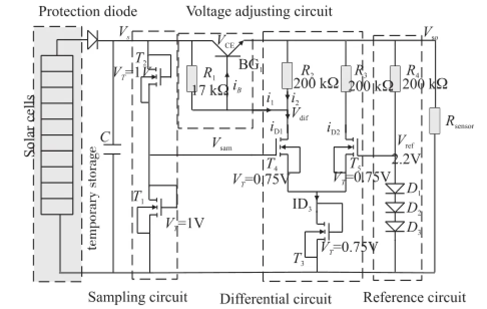
Fig.1 schematic diagram of temporary storage photoelectric Micro-power[12]
In temporary storage photoelectric Micro-power,the main circuits that make up the system include NMOS field-effect transistors,triodes,diodes,resistors,capacitors,photoelectric cells.The basic structure of devices is shown in Fig.2.

Fig.2 Structure of main device of system
The structure of each device shares some similari⁃ty.For example,the emitter region of NPN transistor,the drain electrode and source electrode region of NMOS field-effect transistor and the bottom plate of ca⁃pacitor have the same doping characteristic.The dop⁃ing characteristics of NPN transistor’s base region are the same as that of NMOS field-effect transistor’s P well region.The preparation of N+region in N+/P type photoelectric cell and the preparation of emitter region in NPN transistor also have the same doping character⁃istics.Therefore,the preparation of devices of tempo⁃ rary storage photoelectric Micro-power supply has a good process foundation for on-chip integration.
2 Research on the Process of Tempo⁃rary Storage Photoelectric Micro-Power Integrated On-Chip
2.1On-chip integration scheme of photoelectric Micro-power
According to the basic principle of on-chip inte⁃gration of different devices,on-chip integration schemeof photoelectric Micro-power supply is made to meet the following requirements.①The conversion efficien⁃cy of photoelectric cell should be as high as possible;②The characteristics of devices in energy management circuit should meet the demands of circuit;③Electric isolation should be realized between photoelectric cells and other devices;④The preparation process of photo⁃electric cell should be fully or partially compatible with that of other components.
Considering the photoelectric Micro-power supply system mainly includes NMOS field-effect transistor,NPN transistor,resistors,capacitors,diodes and photo⁃electric cells,The P-type silicon materials with the doping concentration of 5.5×1015cm-3are used,photo⁃electric cell and the on-chip integration of energy man⁃agement circuit is designed based on SOI chip,in or⁃der to improve the compatibility of integrated process. Apart from photolithographic process,the integrated preparation scheme includes seven main process steps,as are shown in Table 1.
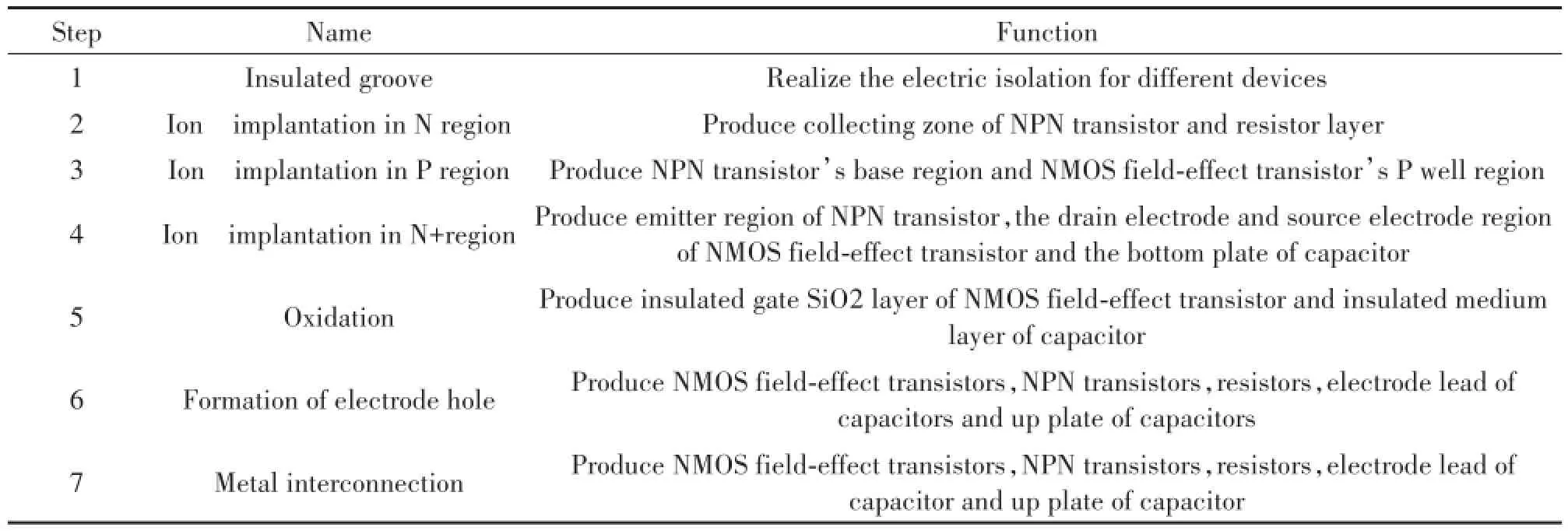
Table1 On-chip integration scheme of photoelectric Micro-power
2.2Function and characteristics of main process steps
Preparation insulated groove to realize electric iso⁃lation for different devices.The preparation of insulat⁃ed groove mainly includes:graphics determination,groove etching,oxide growth,medium backfill and oth⁃er process.
Ion implantation,including ion implantation in N, P,N+region,is the key step that influences the struc⁃ture and characteristics of integrated devices.It is mainly used to prepare the N+/P-type pn junction need⁃ed for Preparation photoelectric cells,P well region,drain electrode and source electrode region of NMOS field-effect transistor,emitter region,base region and collecting zone of NPN transistor and so on.Parameters of ion implantation are shown in the following table:

Table2 Parameters of ion implantation
According to the energy parameters of ion implan⁃tation,it is a low-energy ion implantation,which is ap⁃proximately equivalent to active diffusion based on the relevant theory[13-14].

When boundary conditions are met,the answer to the equation is shown in formula(2).

In the formula,Q is ion implantation dose,D is ion diffusion coefficient,t is diffusion time and x is junction depth.
According to parameters of ion implantation,con⁃centration distribution of corresponding regions in pho⁃toelectric cells(pn junction),NMOS field-effect tran⁃sistor and NPN transistor could be obtained,as is shown in Fig.3(a)(b)(c).The main characteristic pa⁃rameters in diffusion region are shown in Table 3.

Fig.3 Distribution diagram of ionic concentration of main device

Table3 Parameters of ion implantation
Oxidation process:it is used to produce the insu⁃lated gate of NMOS field-effect transistor as well as the insulated medium layer of capacitor.SiO2layer of 100nm is formed on the surface of silicon when silicon reacts with oxygen-containing material(such as oxy⁃gen,water vapor)through thermal oxidation.
Formation of electrode:It is used to produce NMOS field-effect transistor,NPN transistors,resis⁃tors,electrode lead of capacitors and up plate of capaci⁃tors.
Structural model of NMOS field-effect transistor,NPN transistor,photoelectric cell,capacitor,and resis⁃tor in on-chip integration scheme of photoelectric Mi⁃cro-power supply is shown in Fig.4.

Fig.4 Integrated structure of some devices in photoelectric micro-power
3 Main Characteristics of Compo⁃nents Temporary-Storage Photo⁃electric Micro-Power Integrated On-Chip
The main structural parameters of photoelectric cell,NMOS field-effect transistors,NPN transistors, resistor,and capacitor in on-chip integration scheme of photoelectric Micro-power supply are shown in Ta⁃ble 4.
3.1Characteristic of photoelectric cell
In Table 4,implantation junction depth of N+ion in emitter region of photoelectric cell is 0.126μm,dop⁃ing concentration of emitter region is 2.93×10²⁰/cm3,doping concentration of base region is 5.5×10¹⁵/cm3,substrate thickness is 30μm.Simulation analysis is conducted in PC1D.The I-V,I-P characteristic of pho⁃toelectric cell is shown in Fig.5.
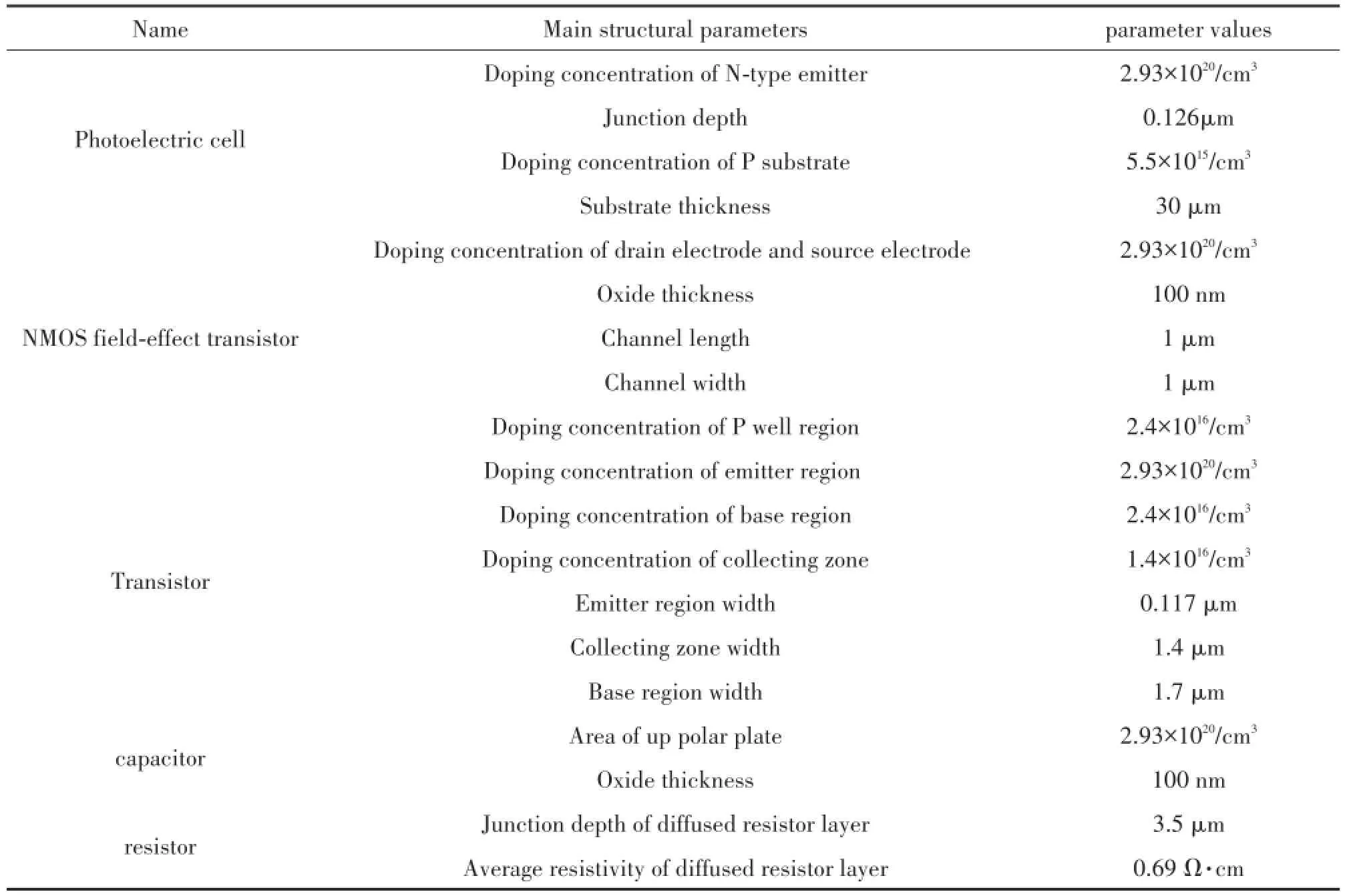
Table4 Main structural parameters of integrated devices

Fig.5 I-V,I-P characteristic of photoelectric cell
You can see from the Fig.5 that the conversion ef⁃ficiency of photoelectric cell designed by integrated process is 9.7%.The voltage and current at maximum power point is 0.44 V and 2.21 A.
3.2Characteristic of NMOS field-effect transistor
Structural parameters(as are shown in Table 3)of NMOS field-effect transistor produced in line with inte⁃gration scheme,threshold voltage and reverse break⁃down voltage are shown in formula(3),(4)based on relevant saturation theories.


In the formula,NAis the doping concentration of well region.Eg is the band gap of substrate at room temperature.As to silicon substrate,Eg is about 1.12 eV.KSis silicon dielectric constant(11.8 F/m).KSis di⁃electric constant of oxide layer(3.9 F/m).ε0is dielec⁃tric constant of air(8.85×10⁻¹²F/m).x0is thickness of gate oxide.ФFis a constant.
The thickness of gate oxide is 0.1 μm.The thresh⁃old voltage of NMOS field-effect transistor eVTand VBD(reverse breakdown voltage of drain electrode)are 0.98 Vand 31.97 V,respectively.
3.3Characteristic of NPN transistor
In temporary storage photoelectric Micro-power,NPN transistor is used as compensating pipe.Accord⁃ing to relevant theory[9]of transistor’s characteristic and the structural parameters(as are shown in Table 4)of transistor produced in photoelectric Micro-power,β is about 83,VBeb(reverse breakdown voltage of emitterjunction)is 31.97 V,VBcb(reverse breakdown voltage of collector junction)is 47.89 V.The breakdown voltage between emitter and collector is 12 V.
3.4Characteristic of resistor
According to relevant theory[10]of diffused resis⁃tor,R□(the sheet resistance in diffused resistor area in photoelectric Micro-power)is 2.2 kΩ/□.The maximum working current of unit resistance width is 0.038 mA. In terms of producing 300 kΩ resistor,the maximum permissible current is 0.025mA.W(minimum width of resistor)is 1 μm;L(length of resistor)is 85 μm.
3.5Characteristic of capacitor
According to relevant theory of MOS capacitor,when the oxide thickness is 100 nm,the per unit area capacitance is:

Therefore we can realize the preparation of capaci⁃tor with differentcapacity by changing the capacitor size.
In short,according to the process characteristics of photoelectric Micro-power,structure and characteris⁃tics of different devices,we can see that the devices produced based on process of photoelectric micro-pow⁃er,including photoelectric cell,NMOS field-effect tran⁃sistor,NPN transistor,resistor and capacitor,meet the requirement of system design.
4 Conclusion
On-chip integration scheme of photoelectric Mi⁃cro-power supply based on SOI chip is proposed ac⁃cording to the structure and process characteristics of devices in temporary storage photoelectric micro-pow⁃er.The process includes seven major steps.The prepa⁃ration process is of good compatibility.In addition,analysis of device characteristics is made based on onchip integration scheme.Experimental results show that the conversion efficiency of photoelectric cell is 9.7%,the threshold voltage and reverse breakdown voltage of drain electrode for NMOS field-effect transis⁃tor is 0.98 V and 31.97 V respectively.The current magnification of NPN triode is 83 and breakdown volt⁃age between emitter and collector is 12 V.The integrat⁃ed devices meet the system requirements.The tempo⁃ rary storage photoelectric micro-power supply could re⁃alize on-chip integration.The integration scheme of photoelectric micro-power supply is feasible.
[1]Singh P,Kaneria S,Anugonda V S,et al.Prototype Silicon Micro-Power Supply for Sensors[J].Sensors Journal,IEEE 2006,6(1):211-222.
[2]Warneke B A,Scott M D,Leibowitz B S,et al.an Autonomous 16 mm3Photoelectric-Powered Node for Distributed Wireless Sensor Networks Sensors[C]//Proceedings of IEEE.200,2(2):1510-1515.
[3]LaFollette R M,Harb J N,Humble P.Microfabricated Secondary Batteries for Remote[C]//Battery Conference on Autonomous,Electronic Devices,Applications and Advances.2001:349-354.
[4]ChenJ M,Liang Y,Cheng D H.The Micro-energy Collecting Tech⁃nology Based on Solar Energy[J].Journal of North China Institute of Water Conservancy and Hydroelectric Power,2012(2):79-81.
[5]Chen Z,Luo P,Yue W J,et al.an Energy-Aware Topology Control Algorithm for Wireless Sensor Networks[J].Chinese Journal of Sensors and Actuators,2013(3):382-387.
[6]Guilar N J,Kleeburg T J,Chen A,et al.Amirtharajah,R.Integrat⁃ed Photoelectric Energy Harvesting and Storage[J].Very Large Scale Integration(VLSI)Systems,IEEE Transactions on,2009,17(5):627-637.
[7]Qin Chong,Yuan Weizheng,Qiao Dayong.Development Summary of Micro Energy[J].Optoelectronic Technology,2005(4):218-221.
[8]Danilov D,Niessen R A H,Notten P H L.Modeling All-Solid-State Li-Ion Batteries[J].Journal of the Electrochemical Society,2011,158(3):A215-A222.
[9]Colby Lenn Bellew.An SOI Process for Integrated Photoelectric Power Circuitry and Actuators for Autonomous Micro-Electrome⁃chanical Systems[M].United States:University of California Berkeley,2002.
[10]She Y,Wen Z Y,Zhao X Q,et al.The MEMS Vibration Energy Harvester with Piezoelectric Array[J].Chinese Journal of Sensors and Actuators,2014(8):1033-1037.
[11]Zhang D,Zhamg S.Improved Electromagnetic Energy Harvest⁃ing from Low-Frequency Vibrations by Closed Magnetic Circuit[J].Chinese Journal of Sensors and Actuators,2015(7):1092-1096.
[12]Xiao L X,He Y T,Liu J H.Research on Energy Management and System Design for I8ntegrated Photovoltaic(PV)Micro Power with the Energy Buffer[J].Electrical Measurement&Instrumentation,2015,52(7):46-50.
[13]Li W W,Wnag S L,Liu Y L.Microelectronics Technology Founda⁃tion[M].Beijing:Chemical Industry Press,2007.
[14]Hao Y,Jia X Z,Wu Y G.Introduction to Microelectronics[M]. Beijing:Higher Education Press,2003.

Xiao Lixian(1971-),female,born in YunNan province,China.She received the B.S from YunNan Normal University,China,in 1995,M.S degree from unNan Normal University,in 2005,respectively. She is currently a associate professor at chuxiong normal university.He has been engaged Optoelectronic technology,micropower supply technology and MEMS technology;

He Yongtai(1970-),male,Correspond⁃ing author,born in YunNan province,China.He received the B.S from YunNan Normal University,China,in 1995,M.S degree from Kunming Institute of Tech⁃nology and Ph.D degree in Beijing Insti⁃tute of Technology in 2005 and 2010,respectively.He is currently a professor at chuxiong normal university.He has been engaged Opto⁃electronic technology,micro-power supply technology and MEMS technology,hyt_127@163.com;

Liu Jinhao(1985-),male,born in Yun⁃Nan province,China.He received the B.S from Changchun University,China,in 2007,M.S degree from Shanxi University of science&technology,China,in 2010. He is currently a lecturer Lecturer at chuxiong normal university.He has been engaged Optoelectronic technology and solar energy application;

Li Lei(1983-),male,born in Shanxin province,China.He received the B.S from Chuxiong Normal University,China,in 2007,M.S degree from Yunnan Normal University,China,in 2010.He is currently a Lecturer Lecturer at chuxiong normal uni⁃versity.He has been engaged Optoelectron⁃ic technology and solar energy application.
EEACC:723010.3969/j.issn.1004-1699.2016.06.008
片上集成光电微能源工艺兼容性及器件特性研究*
肖丽仙,何永泰*,刘晋豪,李雷
(楚雄师范学院物理与电子科学学院,云南楚雄675000)
根据暂存式光电微能源系统组成器件的制备工艺特点,提出了基于SOI晶片的光电微能源片上集成方案。主要工艺包括绝缘沟槽刻蚀、离子注入、氧化等,具有较好的制备工艺兼容性。另外,根据片上集成方案,对器件特性进行了研究。结果表明,光伏电池的转换效率为9.7%,NMOS管阈值电压、漏极反向击穿电压VT分别为0.98 V和31.97 V,NPN三极管的电流放大倍数、集电极-发射极之间击穿电压约为83 V和12 V。各器件特性满足系统工作要求,集成方案具有较好的可行性。
光电微能源;片上集成;工艺方案;兼容性;器件特性
TN453
A
1004-1699(2016)06-0834-07
2015-12-16修改日期:2016-02-16
项目来源:National Natural Science Foundation of China(61271159);Education Department Major Project Foundation of Yunnan Province(zb2014014)
- 传感技术学报的其它文章
- Construction of a Cell Impedance Biosensor Based on Graphene Oxide/Polypyrrole-Indium Tin Oxide Micro-Electrode for Detecting Cell Adhesion and Proliferation*
- Acetone Gas Sensor Based on Al-Doped ZnO and Influence of Ultraviolet Excitation on Gas-Sensing Properties*
- Research of Fusion Classification of EEG Features for Multi-Class Motor Imagery*
- An Improved Method for Noninvasive Detection of Blood Glucose of Conservation of Energy Metabolism*
- Genetic Algorithms of Electromagnet in Longitudinal Wave Electromagnetic Utrasonic Dtection for Auminum Pate*
- Simulation and Experimental Investigation of Thickness Measurement Using Pulsed Eddy Current Technique*

