
Alumina Photonic Crystals with Defect Modes for Sensor Application
2014-07-19 11:17:08PengYanGuangTaoFeiHuiLiGuoliangShangBingWuLideZhang
Peng Yan,Guang-Tao Fei,Hui Li,Guo-liang Shang,Bing Wu,Li-de Zhang
a.Department of Physics,University of Science and Technology of China,Hefei 230026,China
b.Binzhou Medical University,Yantai 264300,China
c.Key Laboratory of Materials Physics and Anhui Key Laboratory of Nanomaterials and Nanostructures, Institute of Solid State Physics,Hefei Institutes of Physical Science,Chinese Academy of Sciences, Hefei 230031,China
Alumina Photonic Crystals with Defect Modes for Sensor Application
Peng Yana,b,c,Guang-Tao Feic∗,Hui Lia,c,Guo-liang Shangc,Bing Wuc,Li-de Zhangc
a.Department of Physics,University of Science and Technology of China,Hefei 230026,China
b.Binzhou Medical University,Yantai 264300,China
c.Key Laboratory of Materials Physics and Anhui Key Laboratory of Nanomaterials and Nanostructures, Institute of Solid State Physics,Hefei Institutes of Physical Science,Chinese Academy of Sciences, Hefei 230031,China
One-dimensional alumina photonic crystals with defect modes were successfully fabricated through inserting a constant voltage waveform into the periodic voltage signals.The transmission spectra show that the thickness of defects plays a key role in determining the transmittance of defect modes.When the thickness was~180 nm,an obvious defect mode with the high transmittance of 55%and a narrow full width at half maximum of 18 nm was observed in the original photonic band gaps.The defect mode shifted linearly with the increasing of refractive index of the analytes infiltrated into pores,indicating its potential application in chemical sensing or bio-sensing.
Nanomaterial,Porous material,Alumina,Photonic crystal,Sensor
I.INTRODUCTION
Photonic crystals(PCs),a kind of special periodic structures containing ordered arrays with high and low dielectric constant components,have attracted a great amount of attention due to their ability to control the propagation of electromagnetic waves and their potential applications in optoelectronic or optical communications[1-5].Alumina is considered as one of the most promising materials for making PCs with air because alumina’s refractive index(~1.7)is higher than that of air(~1).In 1999,anodic aluminum oxide(AAO)with photonic band gaps(PBG)was f i rst reported by Masuda[6].Recently,Wang et al.applied a periodically varying anodic voltage to fabricate alumina PCs[7],its PBG position could be tuned by altering chemical etching time.Hu et al.[8]and Zheng et al.[9]subsequently discussed optical properties of this type of alumina PCs. To control pore structure,pulse and cyclic anodization methods were also developed by Lee et al.[10]and Losic et al.[11],respectively.
All these work mainly focused on the fabrication of perfect PCs without defects.Introducing defects structure into a conventional PC will result in a localized defect mode inside the original PBG[12,13].With the point-,line-or planar-defects,light can be guided and conf i ned in the defects.Alumina PCs with defects may be more valuable,since defects could supply more freedom to control the behavior of photon.However,up to now,the reports about defects-introduced alumina PCs are still less[14-16].
In this work,alumina PCs with planar defects was fabricated by inserting a constant voltage into the periodically varying anodic voltage signal.The defect structure,i.e.a straight pore,will result in the appearance of defect modes in the PBG.The results show that the position of defect modes has a linear relation with the liquid analytes injected into the alumina PCs,revealing the possibility as a sensor.
II.EXPERIMENTS
The detailed pre-treatment of aluminum foils was recorded in Ref.[17].Alumina PCs were prepared through a modi fied two-step anodization method.The fi rst anodization of aluminum foils was conducted under 53 V for 3 h in 0.3 mol/L H2C2O4solution at 4◦C and subsequently it was immersed in the aqueous solution of 5%H3PO4and 1.8%H2CrO4for 4.5 h to remove the formed alumina on the surface.The second anodiztion was carried out in the same electrolyte at 18◦C under a periodic voltage by a programmed power supply.Finally,the samples were etched with saturated CuCl2solution to remove the residual aluminum on the back side.All of anodization process was performed for 400 cycles.The morphologies of the asprepared alumina samples were characterized by a fieldemission scanning electron microscopy(FESEM,Sirion 200),and the transmission spectrum was measured by a spectrophotometer(CARY-5E)with the incident light perpendicular to the sample surface.In order to explore the feasibility as a chemical sensor,alumina PCswere soaked into a series of analytes,including water (n=1.333,where n represents refractive index),ethyl alcohol(n=1.3618),and ethylene glycol(n=1.4318).Before the optical transmission spectrum was measured by a UV-VIS-NIR spectrophotometer(UV3600),alumina PCs were soaked in the analytes for 15 min to minimize the measuring uncertainty.All chemicals were analytical grade and used without further purif i cation.
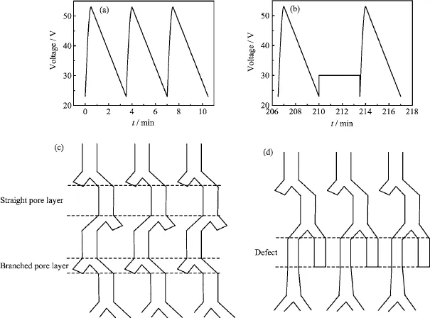
FIG.1 (a)The waveform of a periodic anodic voltage,(b)the defect-introducing voltage waveform(constant voltage), (c)schematic illustration of the pores of alumina PCs formed under the periodic voltage,and(d)schematic illustration of the pores of alumina PCs with defect created by the constant voltage Vdof 30 V,which is marked by two dash lines.
III.RESULTS AND DISCUSSION
The periodic anodic voltage was employed to prepare the anodic alumina PCs with defects.In each cycle, the applied voltage increases sinusoidally from 23 V to 53 V in 30 s and then decreases linearly from 53 V to 23 V in 180 s,as shown in Fig.1(a).After the anodization was performed for 60 cycles,a constant voltage of 30 V was inserted as shown in Fig.1(b),and the duration time could be set to different value.It is reported that the pore diameter is proportional to the oxidation voltage and Y-branched pores can be formed when the oxidation voltage reduced to a factor of 2-1/2(~0.71)[7].Figure 1(c)shows the schematic diagram of pores of alumina PCs prepared under the voltage wave in Fig.1(a).Branched pore layers form in the low voltage stage,while high voltage leads to the formation of straight pore layers[9].Besides,the planar defect marked by two dashed lines in Fig.1(d)can be induced at the desired position when constant voltage Vdwas applied,and the length and the pore diameter could be easily tuned by altering the duration time and the value of the constant voltage.
Figure 2 shows the surface and cross-sectional scanning electron microscopy(SEM)images of the alumina PCs under Vdof 30 V with duration time of 3 min.The top view of SEM image(Fig.2(a))demonstrates that the diameter of the pore is 80-110 nm.The cross-sectional SEM image(Fig.2(b))illustrates that a periodic structure with straight pore layers and branched pores layers is formed.Here,the straight pore layer formed under the Vdof 30 V acts as defects,which is marked by two lines in Fig.2(b).The length of the defect is~180 nm, which could be easily tuned by altering the duration time of Vd.The pore diameter and interpore distance of the defect layer,determined by the value of Vd,is about 35-60 and 84 nm,respectively.
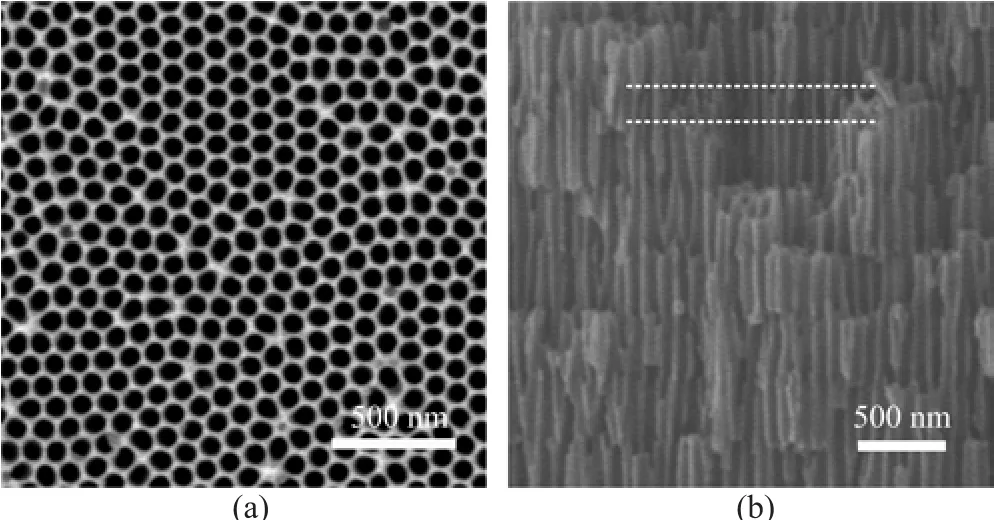
FIG.2 SEM images of(a)the surface and(b)cross-section of the as-prepared alumina PCs.The defect layer was marked by the two lines.

FIG.3(a)Transmission spectra of alumina PCs with and without defects.Alumina PCs without defects(dash line) have an obvious PBG.The defect leads to the appearance of the defect mode(solid line).(b)Transmission spectra of alumina PCs with different duration time under constant voltage Vdof 30 V.
The spectral characteristics of transmission light were investigated with incident light perpendicular to the sample surface.Figure 3(a)shows the influence of the defects on the transmission spectra of alumina PCs. Dash line corresponds to the alumina PCs without defects,and the PBG is clearly visible.The transmission spectrum of alumina PCs with defects created by the Vdof 30 V lasting for 3 min is also shown.It can be concluded that an obvious defect mode,resulting from the defect layer,exists in the original PBG.For comparison,the transmission spectra of the defect-containing alumina PCs with different duration time of 1,3,and 5 min under Vdof 30 V are shown in Fig.3(b).It can be found that all of the band edge of the PBG starts from~805 nm.For the sample with the duration time of 3 min,an obvious defect mode appears in the original PBG,the transmittance and full width at half maximum(FWHM)of which reaches to 55%and 18 nm, respectively.For the samples with the duration time of 1 and 5 min,the remarkable defect mode is not found in the transmission spectra.Therefore,the thickness of the defect layer has signif i cant influence on the existence of the defect mode.
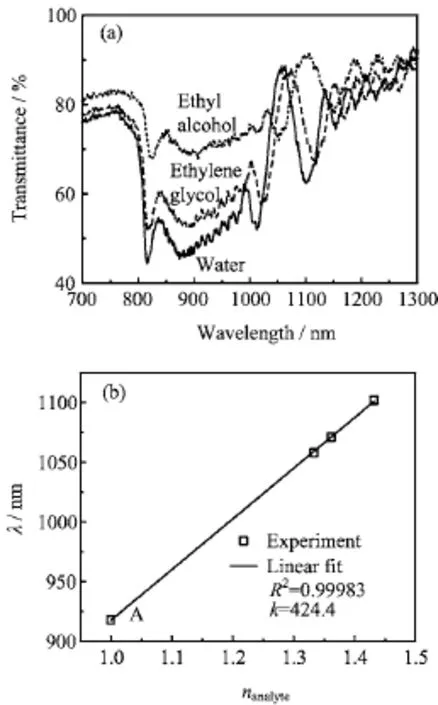
FIG.4(a)Transmission spectra of alumina PCs soaked in water(n=1.333),ethyl alcohol(n=1.3618),and ethylene glycol(n=1.4318).(b)The dependence of the position of the defect mode on the refractive index of various liquid.“A”corresponds to the solid line in Fig.3(a).
The defect-containing alumina PC has a narrow FWHM which can be used as a sensor for the analytes identif i cation.Figure 4(a)is transmission spectra of the alumina PC(Vdlasting for 3 min)soaked in different liquids,including water(n=1.333),ethyl alcohol (n=1.3618),ethylene glycol(n=1.4318).The position of the defect mode has a red shift when increasing the refractive index of liquids.For one-dimensional PCs, the position of PBG can be described by the following equation[9]:

where λmis the central position of PBG(m is the order of the Bragg condition);nHand nLstand for the effective refractive index(ERI)of straight and branched pore layer,while dHand dLare the thickness of straight and branched pore layer.The evaluation of ERI can be estimated using effective medium approximations[17]:
where P is porosity,neffis the ERI of porous alumina, nAl2O3is the refractive index of Al2O3,nairis the refractive index of air(nair=1).When alumina PCs were soaked in analytes,air in pores gave way to those liquids with larger refractive index,leading to the increase of the ERI of both branched and straight pore layers according to Eq.(2).Therefore,based on Eq.(1),the PBG and defect modes shifted to a longer wavelength direction.Because the accurate identif i cation of the PBG central position is very difficult in Fig.4(a),we used the defect mode position to evaluate the transmission spectra changes.Figure 4(b)shows the variation of central wavelength of the defect mode as a function of the refractive index of analyte.The central wavelength λ of the defect mode exhibited linear relationships with the refractive index n of analyte.The slope of the curve(∆λ/∆nanalyte)indicates the sensitivity of alumina PCs on liquid type with different refrative index.The greater∆λ/∆nanalyte,the more signif i cant the shift of defect modes,and the easier the detection of liquid.Here,∆λ/∆nanalyteis 424.4 for the series of analytes,increasing almost 300%in the sensitivity to analytes compared to 108.5 reported in Ref.[18].On the other hand,by measuring the transmission spectra,the refractive index of analytes can be roughly estimated based on the slope(∆λ/∆nanalyte).Further,the alumina PCs can be modif i ed with an organic molecule and used as a platform facing chemical or biological sensing and recognition by monitoring the variation of the defect mode position.
IV.CONCLUSION
In this work,the planar defect was successfully introduced into the alumina photonic crystals through inserting a constant voltage into the periodic voltage signal.The results show that the planar defect with a certain thickness can lead to the appearance of the defect mode in original PBG.The defect mode has a very narrow FWHM and its shift caused by the environment can be more easily recognized.Therefore the alumina PCs with defect modes may be used as a sensor responding to the substance injected into the pores.
V.ACKNOWLEDGMENTS
This work was supported by the National Basic Research Program of China(No.2012CB932303), the National Natural Science Foundation of China (No.11074254 and No.51171176),Hundred Talent Program of Chinese Academy of Sciences,and the President Foundation of Hefei Institute of Physical Sciences.
[1]Z.Z.Wu,D.Lee,M.F.Rubner,and R.E.Cohen, Small 3,1445(2007).
[2]B.V.Lotsch and G.A.Ozin,Adv.Mater.20,4079 (2008).
[3]D.P.Puzzo,L.D.Bonifacio,J.Oreopoulos,C.M.Yip, I.Manners,and G.A.Ozin,J.Mater.Chem.19,3500 (2009).
[4]B.M.Gonz´alez,G.Christie,C.A.B.Davidson,J. Blyth,and C.R.Lowe,Anal.Chim.Acta 528,219 (2005).
[5]G.G.Rong,J.D.Ryckman,R.L.Mernaugh,and S. M.Weiss,Appl.Phys.Lett.93,161109(2008).
[6]H.Masuda,M.Ohya,H.Asoh,M.Nakao,M.Nohtomi,and T.Tamamura,Jpn.J.Appl.Phys.38, L1403(1999).
[7]B.Wang,G.T.Fei,M.Wang,M.G.Kong,and L.D. Zhang,Nanotechnology 18,365601(2007).
[8]X.Hu,Z.Y.Ling,S.S.Chen,and X.H.He,Chin.Phys. Lett.25,3284(2008).
[9]W.J.Zheng,G.T.Fei,B.Wang,and L.D.Zhang, Nanoscale Res.Lett.4,665(2009).
[10]W.Lee,K.Schwirn,M.Steinhart,E.Pippel,R.Scholz, and U.G¨osele,Nat.Nanotechnol.3,234(2008).
[11]D.Losic,M.Lillo,and D.Jr.Losic,Small 5,1392 (2009).
[12]W.Q.Ding,L.X.Chen,and S.T.Liu,Opt.Commun. 246,147(2005).
[13]R.Geiss,S.Diziain,R.Iliew,C.Etrich,H.Hartung, N.Janunts,F.Schrempel,F.Lederer,T.Pertsch,and E.B.Kley,Appl.Phys.Lett.97,131109(2010).
[14]F.Intonti,S.Vignolini,V.Trck,M.Colocci,P.Bettotti,L.Pavesi,S.L.Schweizer,R.Wehrspohn,and D. Wiersma,Appl.Phys.Lett.89,211117(2006).
[15]A.Yokoo,M.Notomi,H.Suzuki,M.Nakao,T.Tamamura,and H.Masuda,IEEE J.Quantum Elect.38,938 (2002).
[16]P.Yan,G.T.Fei,Y.Su,G.L.Shang,H.Li,B.Wu, and L.D.Zhang,Electrochem.Solid State Lett.15, K23(2012).
[17]P.Yan,G.T.Fei,G.L.Shang,B.Wu,and L.D.Zhang, J.Mater.Chem.C 1,1659(2013).
[18]D.L.Guo,L.X.Fan,F.H.Wang,S.Y.Huang,and X.W.Zou,J.Phys.Chem.C 112,17952(2008).
ceived on August 8,2013;Accepted on September 16,2013)
∗Author to whom correspondence should be addressed.E-mail:gtfei@issp.ac.cn,Tel.:+86-551-65591453,FAX:+86-551-65591434
 CHINESE JOURNAL OF CHEMICAL PHYSICS2014年1期
- CHINESE JOURNAL OF CHEMICAL PHYSICS的其它文章
- Experimental and Theoretical Investigation on Excited State Intramolecular Proton Transfer Coupled Charge Transfer Reaction of Baicalein
- Theoretical Study of Reagent Rotational Excitation effect on the Stereodynamics of H+LiF→HF+Li Reaction
- Infrared Spectroscopy of COIsolated in Solid Nitrogen Matrix
- effects of Rotational Isomerism and Bond Length Alternation on Optical Spectra of FTC Chromophore in Solution
- High Pressure Structural Instability and Thermal Properties of Rutile TiO2from First-principles
- Kinetic Implication from Temperature effect on Hydrogen Evolution Reaction at Ag Electrode