
effect of Ar+,He+,and S+Irradiation on n-InP Single Crystal
2014-07-19 11:17:08JingyuHuWaqasMahmoodQingZhao
Jing-yu Hu,Waqas Mahmood,Qing Zhao
School of Physics,Beijing Institute of Technology,Beijing 100081,China
effect of Ar+,He+,and S+Irradiation on n-InP Single Crystal
Jing-yu Hu,Waqas Mahmood,Qing Zhao∗
School of Physics,Beijing Institute of Technology,Beijing 100081,China
The irradiation effects of Ar+,He+and S+with energy from 10 eV to 180 eV on n-InP(100) surface are analyzed by X-ray photoelectron spectroscopy and low energy electron diffraction. After irradiation on the n-InP surface,damage on the surface,displacement of the Fermi level and formation of sulfur species on S+exposed surface are found and studied.Successive annealing is done to suppress the surface states introduced by S+exposure.However,it is unsuccessful in removing the damage caused by noble ions.Besides,S+ions can efficiently repair the Ar+damaged surface,and f i nally form a f i ne 2×2 InP surface.
Low energy ion bombardment,Annealing,Surface damage,Fermi level
I.INTRODUCTION
Since sulf i de passivation was f i rst introduced by Sandrof fet al.in 1987[1,2],in the dry etching and industrial processes,much attention has been paid to reducing native oxide layers and removing the ion irradiation damage from III-V semiconductors[3-6].It has also been reported that sulfur brings together atoms on the n-InP surface and the strong bond between S and In keeps bonding and the anti-bonding states away from the band gap[7,8].Several different methods have been employed for passivation of sulf i de,such as treatment with solutions[4-6,9-14]and gas phase[15-20].The process of dissolving III-V semiconductors using solutions is rather slow and terminates in forming a 1×1 surface[21].For the gas treatments,annealing is compulsory to retrieve the 1×1 surface[22].Sulf i de assists the formation of ordered structure,and experimental results also elucidated that polysulf i des render better passivation on III-V surfaces for both solution and gas treatments[21,23].This leads to an understanding that the surface might supply electrons to sulfur atoms that is partially supported by the high reactivity of n-type semiconductors as compared to p-type semiconductors [24].Thus,the surface can use additional available energy for passivation of sulfur.For p-InP surface,type inversion has also been reported[24,25].Recently,electron energy loss spectroscopy(EELS)has been used to investigate the interactions between the low energy Ar+(N+)ions and the InP compound[26].The InP surface is extremely sensitive to Ar+ions bombardment.If the surface is exposed in Ar+ions fluence for longer time, the chemical bond In-P will be breaken and the In metal will appear on the surface accompanied with the formation of structural physical defects.Usanmaz et al.[27]studied the changes in the electronic and structural properties appearing from S adsorption on the GaAs(001)surface by the ab initio calculations and observed that the Tsukamoto model is energetically most stable.
High ions flux plasma with an average ion energy below 10 eV has been used[28].If we are able to properly understand the interaction mechanism and the extent of surface damage during ion irradiation of compound semiconductors,novel ion assisted processes can likely be developed to resolve some of the current problems related to surface damage of ion irradiation in device fabrication.To f i nd a method that fully controls the reaction products between ions and III-V semiconductors, in this work we irradiate a controlled low energy Ar+, He+,and S+ions beam onto a n-InP(100)surface,and study the interactions of ions with n-InP(100)surface in detail.We also compare different effects of inert and S+ions bombardment on InP surface.
II.EXPERIMENTS
Low energy ion beam system(LEIB)[29]has been used to expose ions on the samples.The ion beam system is directly connected to the ultra high vacuum (UHV)surface analysis apparatus.The sample travels through the vacuum chambers with the aid of transfer rods.The analysis equipment has two parts:the standard Kratos AXIS-HS XPS and the low energy electron diffraction(LEED)system.The center of the target retains ion current density of 0.1-1 A/cm2.The XPS system was equipped with a monochromatic X-ray source (Al Kα),and its energy calibration was referenced by Au4f7/2at 84.0 eV,Cu2p3/2at 932.7 eV,and Ag3d5/2at 368.3 eV peaks,respectively.The incident angle of X-ray source was 55◦,and the angle between photoelectron detection and the sample surface was 90◦.
A single un-doped n-InP crystal is used in the experiment,and its observed bulk Fermi level position is at 1.26 eV.The surface of the sample is fi rst treated with UV/O3,then the process of removing oxides is completed in a less concentrated HF solution(1:30 HF:H2O).Further,it is dried using nitrogen,and quickly transported to the analysis chamber.This shipping is done in the surrounding of nitrogen atmosphere. Inside the UHV system,we perform several treatments and measurements on the sample.The sample is transferred to the LEIB system through the UHV passage for ion exposure.After receiving independent fl uence of Ar+,He+,and S+,it is returned to XPS chamber for further investigation.
To investigate samples inside the spectrometer,we consider valence band(VB)edge of gold as a reference to locate other Fermi levels.The distance between the Fermi level of gold and the VB edge of semi-conductor fi nally locate the Fermi position of the samples.After determination of the Fermi level position,we apply the core levels of In3d5/2or P2p3/2as spectral references for locating the Fermi level shifts of other samples.In this work,In3d5/2of InP with high photoelectron emission is used to measure the surface band bending,and locate the Fermi level position.A sample with its Fermi level position at the VB maximum should have the In3d5/2at 444.9 eV for n-InP as our reference,and all Fermi level positions are referred to the VB edge of n-InP.
III.RESULTS AND DISCUSSION
A.effect of He+and Ar+
The irradiation of He+and Ar+ions on n-InP(100) damages the sensitive surface,which is estimated by calculating the binding energy changes of In3d5/2.The result is similar to the case of InP(110)[30],where no additional chemical components are observed in the XPS spectra.Figure 1 displays the e ff ect of He+and Ar+ions irradiation on the n-InP(100)surface as a function of ion fl uence at variable energies.Considering Ar+ions as a reference,it is observed that for the same ion type,surface damage increases with increase of the fl uence.In addition,Ar+ions produce much heavier surface damage than He+ions when the same ion fl uence and energy are used.The 110 eV Ar+can lead the Fermi level to pin position with fulence of 1016ions/cm2while it needs higher dosage(around 3×10¹⁷ions/cm2) to reach the same level by 110 eV He+ions.
Figure 1 clearly reveals the gradual defect formation induced by low energy ion bombardment for various inert ions and energies.The results illustrate that native defects themselves may also lead to band bending and Fermi level pinning,which is similar to several results in Refs.[19,20].
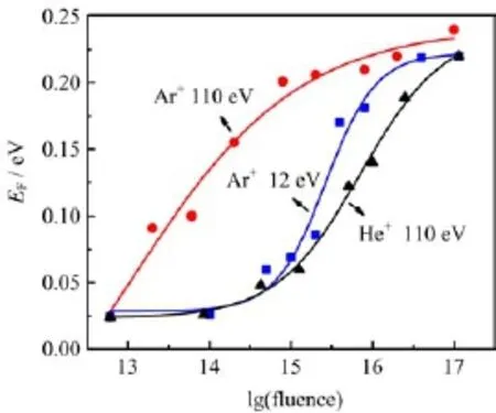
FIG.1 Fermi level EFshifts of n-InP(100)induced by Ar+, and He+ion bombardments with different energies as a function of ion fluence.
B.effect of S+
The results of the surface electrical properties obtained from the irradiation of S+ions on n-InP surface are found to be extremely different from the bombardment of inert ions.In Fig.2,we display the binding energies of In3d5/2and Fermi level shifts,vs.ion fluence and annealing temperature respectively,obtained from the exposure of S+ions at energy values of 12,60, and 110 eV.The plot indicates that for the applied ion energies 12 and 110 eV,the band bending of n-InP increases,however it is slightly decreased at energy 60 eV. Interestingly,the least surface band bending on n-InP is observed not at 12 eV but at 60 eV,which is similar to the previous observation of p-InP[31].It can be inferred from the results that bombardment of ion beam follows two reaction paths:(i)the formation of In-S bonds,and(ii)resistance to physical damage.
Experimentally,it is observed that even low dosage of S+ions(1016ions/cm2)results in the band bending of n-InP surface at both the energy values of 12 and 60 eV.However,with the increasing of S+ions, the surface band bending changes slightly for 60 eV, but it is found to be continuously increasing at 12 and 110 eV.The result at 60 eV conf i rms that S-In species resist physical damage to the surface,but for higher ion energy i.e.110 eV,S-In species can not effectively prevent the heavier damage.More damage at 12 eV than at 60 eV,may be due to the effect of high energy neutral species.When low ion energy 12 eV is used,the density of ion beam current is half less than that of 60 eV S+ions.In order to receive the same ion number as that at 60 eV,irradiation time of S+ions at 12 eV should be twice of that at 60 eV.This long exposure time increases the chances of neutral species to reach the surface.The chemical properties of n-InP and p-InP surfaces are the same,but their electronic properties are different.Sulfur is n-type doping as shown in Fig.3,and its diffusion in p-InP explains type inversion[31].

FIG.2 Binding energy E of In3d5/2and Fermi level EFresponse of n-InP(100)induced by 12,60,and 110 eV S+as a function of(a)ion fluencies and(b)subsequent annealing temperatures,(c)S2p spectrum of n-InP induced by S+bombardment with 1.6×10¹⁶ions/cm2at 60 eV.
However,for n-InP,to move the surface Fermi level near to the minimum of conduction band,donor states matching the initial dopant concentrations are specifically required when the surface Fermi level of n-InP has already been close to the minimum of conduction band.For this reason,only slight changes in the Fermi level have been seen after S+exposure on the n-InP surface.The S+irradiation of 8×10¹⁵ions/cm2modi fies the band bending of the n-InP surface slightly at ion energies 12 and 60 eV,but signi fi cant increase is observed at energy 110 eV.Raising ion fl uence up to 1.2×10¹⁶ions/cm2increases the band bending at 12 and 110 eV while it reduce the band bending at 60 eV.Irradiation at di ff erent ion energies forms In-S species,which limit physical surface damage,and exhibit a donor doping e ff ect for n-InP,therefore reduce the band bending.The band bending at 12 eV increased with the rising of ion fl uence since few In-S species have been created on the surfaces.On the other hand,at 110 eV,although strong In-S species have been created,and the surface band bending increases versus ion fl uence.In this case,higher ion energy causes greater physical damage,which cannot be preventable by In-S species.
C.Comparison of He+,Ar+,and S+
Noble gas ions(He+or Ar+)irradiation only caused physical damage on InP(110)that resulted in a shift of surface Fermi level without any chemical change [30,32].For He+and Ar+,with incident energy of 5-180 eV and fluence of 1012-1017ions/cm2,surface Fermi levels of both n-and p-InP(100)surfaces move towards to their pinning position.This kind of damage is hard to overcome,even through subsequent annealing process[30].However,the chemical reaction in S+ions exposure forms sulfur species(S-In)on InP surfaces that prevent further physical damage,and bring surface ordering in subsequent thermal annealing.During the ion showering,a few sulfur ions possibly reach subsurface layers and produce donor states.The exposure of InP(100)surface to S+ions with 1.5×10¹⁶ions/cm2fl uence at energy values of 10,20,60,70,and 100 eV results in the changes of surface chemical composition (not shown here).Figure 2(c)shows the S2p spectra with fl uence of 1.6×10¹⁶ions/cm2at 60 eV S+ion bombardment.
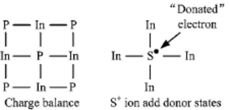
FIG.3 Charge balance and donor states.
The spectral data at different ion energy treatment show the formation of one type of sulfur specie in S2p region.For energy above 60 eV,formation of sulfur species is more efficient.For the same number of ions at 12 eV as that at 60 eV,few sulfur species are found when S+ions are used.This makes obvious that higher energetic S+ions favor creation of In-S species on InP(100) surface as compared to 12 eV ions.At 110 eV,S+exposure results in the broader S2p3/2peak due to higher intensity of S-In formed on the InP surface.However, simultaneously the 110 eV S+also induces heavier disordered surface,which is different from the 60 eV case. Table I lists the atomic ratios of S and P to In at different S+energy values.
Ion bombardment assists the chemical reaction and forms more stable sulfur species(In-S)[22,33,34].According to our previous results of He+and Ar+ion bombardment,there is no chemical interaction between inertial ions and InP surface[30,32].Physical damage is produced during inertial ions bombardment,and Fermi level does not return to the original position after subsequent annealing.However,in the case of annealing InP with UV/O3and HF at 500◦C,LEED pattern was not observed[19],because annealing of InP without S+exposure results in higher As or P loss on the surface. The In-S species on the InP surface not only stabilize the surface against As or P desorption,but also assist re-ordering.
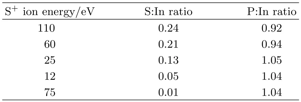
TABLE IThe composition of S+treated n-InP(100) sampleswithdifferentionenergiesandfluenceof 2.0×10¹⁶ions/cm2
D.Behavior of Fermi level of n-InP with annealing
When ions expose on n-InP samples,the surface band bending is found to increase with temperature at all energies.At 300◦C,the band bending of samples exposed at 60 eV is smaller than at 110 eV as shown in Fig.2(b).This behavior is seen for all samples and attributes to sulfur doping or meta-stable bond that might have formed on the surface at low temperature. With an increase in energy,implantation of sulfur becomes deeper into the surface.Subsequent heating from 300◦C to 450◦C reduces the bending of the surface band for entire ion energies.Subsequent annealing at 300◦C causes slight bending of the surface band for 60 eV ion-treated n-InP samples.After annealing at 450◦C,it even exceeds the original surface Fermi level as shown in Fig.2,which means that part of original surface states are removed from the surface due to the annealing process.However,at 110 eV,with S+ion bombardment,where the physical damage is substantial,annealing at 450◦C could not bring the surface Fermi level back to the original position.
E.effect of Ar+and S+ions on the Fermi level of n-InP
In addition,we have experimentally investigated the role of S+irradiation in bringing order on InP surface. The n-InP(100)is f i rst exposed to 180 eV Ar+ions at an incidence angle of 45◦,and after that,to subsequent 60 eV S+ions with different dosages,and f i nally they are annealed at 250,300,and 400◦C.Figure 4 presents the binding energy of In3d5/2and Fermi level movement under aforementioned conditions.Irradiation of 180 eV Ar+ions shifts the Fermi level to 1.04 eV and then,subsequent 60 eV S+ions exposure further decrease the Fermi level to 0.90 eV.With this treatment, Ar+and S+ions create defects at the surface of the Fermi level,and introduce a monolayer equivalent of S simultaneouly.Repeated annealing at temperatures 300 and 400◦C,almost returned Fermi level to its original location and lastly,we obtain a 2×2 LEED pattern as presented in Fig.5.The pattern conf i rms that the presence of sulfur supports surface ordering and recovers the physical damage by ions.

FIG.4Binding energy and Fermi level variation of n-InP(100)with(a)180 eV Ar+ions shower at 45◦incidence,(b)60 eV S+shower,and(c)subsequent annealing at 250,300,and 400◦C.
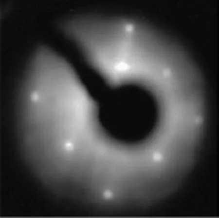
FIG.5 2×2 LEED pattern formed by processes of 180 eV Ar+shower with 45◦incidence,60 eV S+ion-treated n-InP(100),and subsequent annealing at 400◦C for 20 min.
A surface model of In-terminated regions with hydrogen atoms filling the dangling bonds,P-terminated and disordered regions was proposed for the UV/O3and HF treated InP(100)surface[22].When S+with enough energy strikes InP surface,weak H-In bond is replaced by strong S-In bond.Few S atoms replace P atoms, create donor states,and end up forming S-In tetrahedral while few of them reside in the subsurface region as interstitial atoms.For S+ion energy less than 20 eV, the bond between sulf i de and surface is not efficient. A dominant number of S+ions are backscattered from the surface.When the S+energy is high enough such as 110 eV,it produces more physical damage that is not easy to eradicate by annealing though In-S species are created.Subsequent annealing at 300◦C embeds more sulfur atoms,and forms the S-In tetrahedral that further increases the Fermi level.If we compare their stabilities,the sulfur bridge at the top surface layer is more stable than the sulfur tetrahedron that bonds four In atoms in the subsurface region of InP.
In the process of annealing at 400◦C,sulfur atomsreach the surface to form sulfur bridge,and excess of sulfur atoms are desorbed from the surface that results in one monolayer of sulfur residing on the InP surface, which f i nally leads to a clear LEED pattern as shown in Fig.5.Hence,removal of donor states from subsurface region results in the reduction of Fermi level of n-InP. The existence of sulfur bridges at the surface promotes ordering reconstruction of surface,and repairs the damage.
IV.CONCLUSION
The effects of low energy ions(Ar+,He+,and S+) irradiation on n-InP surface are analyzed thoroughly by examining the chemical and surface changes.It is observed that the irradiation of both He+and Ar+by using the aforementioned conditions shifts the Fermi levels of n-InP surfaces.For the same exposure energy, as expected,Ar+ions cause more damage than He+. For the identical ion type,the exposure induce a surface defect density increasing with both ion energy and fluence.It is obvious that sulfur supports surface ordering. The high energy of S+ions causes more damage and forms S-In species.The formed S-In species help preventing the damage produced by S+ions together with ordering the surfaces of InP during subsequent thermal annealing.Besides,the Ar+damaged n-InP surface is exposed to 60 eV S+ion beam.Later,further annealing at 400◦C enables the Fermi level to almost return to its original location.The return of Fermi level to its previous location ensures that S+ions with subsequent annealing removes n-InP surface damage and leads to 2×2 LEED pattern formations.
V.ACKNOWLEDGMENTS
This work was supported by the National Natural Science Foundation of China(No.11275024)and the Ministry of Science and Technology of China (No.2013YQ03059503 and No.2011AA120101).The authors would like to thank Prof.R.W.M.Kwok from the Chinese University of Hong Kong.
[1]C.J.Sandrof f,R.N.Nottenburg,J.C.Bischof f,and R.Bhat,Appl.Phys.Lett.51,33(1987).
[2]E.Yablonovitch,C.J.Sandrof f,R.Bhat,and T.Gmitter,Appl.Phys.Lett.51,439(1987).
[3]V.L.Berkovits and D.Paget,Appl.Surf.Sci.65,607 (1993).
[4]N.G.Wright,C.M.Johnson,and A.G.O’Neill,Sol. Sta.Elec.42,437(1998).
[5]Y.Dong,X.M.Ding,X.Y.Hou,Y.Li,and X.B.Li, Appl.Phys.Lett.77,3839(2000).
[6]R.K.Gebhardt,A.B.Preobrajenski,and T.Chasse, Phys.Rev.B 61,9997(2000).
[7]V.N.Bessolov,Y.V.Zhilyaev,E.V.Konenkova,and M.V.Lebedev,Tech.Phys.43,983(1998).
[8]V.N.Bessolov,M.V.Lebedev,E.B.Novikov,and B. V.Tsarenkov,J.Vac.Sci.Technol.B 11,10(1993).
[9]N.Yokoi,H.Andoh,and M.Takai,Appl.Phys.Lett. 64,2578(1994).
[10]Z.H.Lu,D.Landheer,J.M.Baribeay,L.J.Hung,and W.M.Lau,Appl.Phys.Lett.64,1702(1994).
[11]H.Oigawa,J.F.Fan,Y.Nannichi,H.Sugahara,and M.Odhima,Jpn.J.Appl.Phys.30,L322(1991).
[12]M.V.Lebedev and M.Aono,J.Appl.Phys.87,289 (2000).
[13]S Morikita,T Motegi,and H.Ikoma,Jpn.J.Appl. Phys.38,L1512(1999).
[14]V.N.Bessolov,M.V.Lebedev,and D.R.T.Zahn, Semiconductors 33,416(1999)
[15]M.Cakmak and G.P.Srivastava,Phys.Rev.B 57, 4486(1998).
[16]Z.Zou,X.M.Wei,Q.P.Liu,H.H.Huang,W.S.Sim, G.Q.Xu,and C.H.A.Huan,Chem.Phys.Lett.312, 149(1999).
[17]M.Cakmak and G.P.Srivastava,Appl.Surf.Sci.123, 52(1998).
[18]M.Shimomura,N.Sanada,S.Ichikawa,Y.Fukuda, M.Nagoshi,and P.J.Moller,J.Appl.Phys.83,3071 (1998).
[19]B.K.L.So,R.W.M.Kwok,G.Jin,G.Y.Cao,G.K. C.Hui,L.Huang,W.M.Lau,and S.P.Wong,J.Vac. Sci.Technol.A 14,935(1996).
[20]A.Kapila,X.Si,and V.Malhotra,Appl.Phys.Lett. 62,2259(1993).
[21]H.Hirayama,Y.Matsumoto,H.Oigawa,and Y.Nannichi,Appl.Phys.Lett.54,2565(1989).
[22]R.W.M.Kwok,G.Jin,B.K.L.So,K.C.Hui,L. Huang,W.M.Lau,C.C.Hsu,and D.Landheer,J. Vac.Sci.Technol.A 13,652(1995).
[23]R.W.M.Kwok,L.J.Huang,W.M.Lau,M.Kasrai, X.Feng,K.Tan,S.Ingrey,and D.Landheer,J.Vac. Sci.Technol.A 12,2701(1994).
[24]R.W.M.Kwok and W.M.Lau,J.Vac.Sci.Technol. A 10,2515(1992).
[25]W.M.Lau,S.Jin,X.W.Wu,and S.Ingrey,J.Vac. Sci.Technol.A 9,994(1991).
[26]N.Berrouachedi,M.Bouslama,A.Abdellaoui,M. Ghaffour,C.Jardin,K.Hamaida,Y.Monteil,Z.Lounis,and A.Ouerdane,Appl.Surf.Sci.256,21(2009).
[27]D.Usanmaz,G.P.Srivastava,and M.Cakmak,J.Appl. Phys.108,063713(2010).
[28]E.D.Lu,F.P.Zhang,S.H.Xu,X.J.Yu,P.S.Xu,Z. F.Han,F.Q.Xu,and X.Y.Zhang,Appl.Phys.Lett. 69,2282(1996).
[29]W.M.Lau,X.Feng,S.Sant,I.Bello,K.K.Foo,and R. P.W.Lawson,Nucl.Instrum.Meth.B 59,316(1991).
[30]Q.Zhao,Z.W.Deng,R.W.M.Kwok,and W.M.Lau, J.Vac.Sci.Technol.A 18,2271(2000).
[31]Q.Zhao,G.J.Zhai,and R.W.M.Kwok,Appl.Surf. Sci.253,1356(2006).
[32]Z.W.Deng,R.W.M.Kwok,W.M.Lau,and L.L. Cao,J.Appl.Phys.86,3676(1999).
[33]G.W.Anderson,M.C.Hanf,P.R.Norton,Z.H.Lu, and M.J.Graham,Appl.Phys.Lett.65,171(1994).
[34]M.Shimomura,K.Naka,N.Sanda,Y.Suzuki,Y. Fukuda,and P.J.Moller,J.Appl.Phys.79,4193 (1996).
ceived on April 14,2013;Accepted on September 24,2013)
∗Author to whom correspondence should be addressed.E-mail:qzhaoyuping@bit.edu.cn
 CHINESE JOURNAL OF CHEMICAL PHYSICS2014年1期
- CHINESE JOURNAL OF CHEMICAL PHYSICS的其它文章
- Experimental and Theoretical Investigation on Excited State Intramolecular Proton Transfer Coupled Charge Transfer Reaction of Baicalein
- Theoretical Study of Reagent Rotational Excitation effect on the Stereodynamics of H+LiF→HF+Li Reaction
- Infrared Spectroscopy of COIsolated in Solid Nitrogen Matrix
- effects of Rotational Isomerism and Bond Length Alternation on Optical Spectra of FTC Chromophore in Solution
- High Pressure Structural Instability and Thermal Properties of Rutile TiO2from First-principles
- Kinetic Implication from Temperature effect on Hydrogen Evolution Reaction at Ag Electrode