
EVG公司在SEMICONChina2014展示新的技术解决方案
2014-07-04 03:27
电子工业专用设备 2014年3期
全球领先的晶圆键合及光刻设备供应商EV Group (EVG)日前宣布,为加强中国半导体市场的实力,将在中国推进批量制造工艺解决方案并在上海开设区域总部。
中国目前是世界半导体3D IC 集成和先进封装技术开发与生产的重点地区,抗蚀剂处理是这些制造技术中一种基本的加工程序。为了取得成功并确保在全球的竞争力, 对于中国的制造厂家来说,与拥有设备、技术和专有工艺技术的主要供应商合作,保持其制造能力迅速地由工艺开发向大批量制造过渡便显得十分重要。
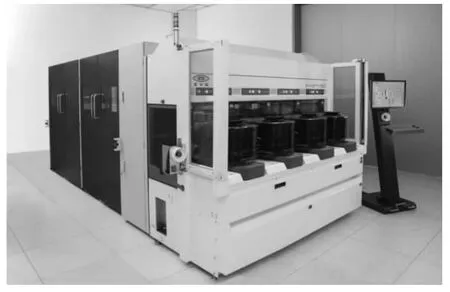
EVG150XT 系统是EVG 公司最新推出的产品,它成功地集合了EVG 公司30 多年在光刻和大批量制造工艺方面的专业知识,率先为客户提供生产意义的大批量制造抗蚀剂处理系统,它能满足在半导体制造中段制程和后段制程中大多数抗蚀剂处理、旋涂介质材料和厚膜的苛刻需求,包括用于2.5D 及3D-IC 集成的封装技术中的硅通孔TSV 成形,晶圆键合、再分布层及转接板制作等用途。
新型EVG150XT 系统是一种通用的全自动抗蚀剂处理机台, 适用于直径到300 mm 的晶圆。为满足不断增长及变化的半导体市场需求,EVG150XT 系统围绕3 个关键方面进行开发:即改进工艺、缩短生产周期、智能软件解决方案来实现复杂、高频率更换工艺流程的需求。
基于XT- 结构设计, EVG150XT 系统的9 个工艺模块,能够同时运行,实现多晶圆并行处理。此外, 该系统还集成了一个在线测量模块, 用以检查各种加工中的不规则性和缺陷,以便进行减少缺陷,提高成品率和降低生产成本的实时工艺修正。
除了推出新的工艺解决方案外, EVG 公司还通过在上海开设新的子公司扩展在中国的业务,新的子公司将作为区域总部进行EVG 公司在中国境内的全部运营业务。新的EVG 中国子公司将具有服务中心和备件管理功能, 以进一步加强EVG 公司在该地区的实力。通过新公司的不断努力,提高对中国客户的服务和响应时间。
详情请咨询位于上海新国际展览中心的EVG公司2451 展台。
EV GROUP STRENGTHENS SUPPORT OF CHINESE SEMICONDUCTOR MARKET WITH VOLUME MANUFACTURING PROCESS SOLUTIONS AND NEW REGIONAL HEADQUARTERS IN SHANGHAI
China is a key region for development and production of leading semiconductor technologies such as 3D-IC integration and advanced packaging. Resist processing is an essential process step for these manufacturing technologies. To be successful and remain globally competitive, it is important for manufacturers in China to partner with key suppliers that have the equipment,technology and process expertise to support their ability to quickly transition from process development into high-volume manufacturing(HVM).
The latest product introduction from EV Group(EVG), called the EVG150XT, successfully combines EVG's expertise of more than 30 years in lithography and HVM processing to provide the first true HVM resist processing system that can meet the most demanding requirements for processing resists, spin-on dielectrics and thick films for mid-end-of-line (MEOL) and back-end-of-line (BEOL) semiconductor applications, including through silicon via (TSV) formation,wafer bumping, redistribution layer and interposer manufacturing for 2.5 and 3D-IC packaging.
The new EVG150XT is a universal and fully-automated resist processing tool supporting wafers up to 300-mm in diameter. To meet the needs of the growing and fluctuating semiconductor market, the EVG150XT was developed around three key aspects:improved processing,short cycle times,and smart software solutions for complex, high-frequency process flows.
Built on the XT-frame architecture, the EVG150XT features nine process modules that can operate simultaneously for multi-parallel wafer processing. In addition, an in-line metrology module has been integrated into the EVG150XT that can detect a variety of process irregularities and defects to enable real-time process corrections to reduce defects, increase yields and lower production costs.
Besides new process solutions, EVG has also expanded its presence in China with the opening of a wholly owned subsidiary in Shanghai, which will serve as regional headquarters for all of EVG's operations in the People's Republic of China. The new EV Group China subsidiary, which houses a local service center and spare parts management facility,further strengthens EVG's presence in the region and supports the company's ongoing efforts to improve service and response times to local customers.
EV Group will exhibit its technology solutions portfolio at SEMICON China, March 18-20, 2014.For more information, please visit EVG at Booth#2451 in the Shanghai New International Expo Center in Shanghai.
猜你喜欢
制冷(2019年2期)2019-12-09
中国电子报(2019年54期)2019-10-24
科学家(2017年20期)2017-11-10
制造技术与机床(2017年2期)2017-05-04
光学精密工程(2016年5期)2016-11-07
光学精密工程(2016年4期)2016-11-07
光学精密工程(2016年3期)2016-11-07
中国惯性技术学报(2015年1期)2015-12-19
中南民族大学学报(自然科学版)(2015年2期)2015-12-16
中国建材科技(2012年5期)2012-01-26
