Role of Gate in Triode-Structure for Carbon Nanotube Cold Cathode
Yong-Qing Guo, Wei-Min Zheng, and Xiao-Juan Zhang
Role of Gate in Triode-Structure for Carbon Nanotube Cold Cathode
Yong-Qing Guo, Wei-Min Zheng, and Xiao-Juan Zhang
—Field emission properties of carbon nanotube cold cathode (CNT-CC) of triode- and diode-structure have been investigated by using the finite element method of numerical simulation. Specially, the effects of gate voltage and hole radiusRon the emission properties have been analyzed based on the finite element method. Results indicate that the gate can make the excitation electric fieldEincrease, turn-on voltage decrease, and the emission current densityJrise. The result shows that theEreaches its maximum value at the top of carbon nanotube (CNT), and the optimum field emission performance can be obtained whenRis equal to 10 times the diameter of the carbon nanotube.
Index Terms—Carbon nanotube, field emission, triode-structure.
1. Introduction
Since the excellent field emission properties of carbon nanotube film firstly was reported by W. A. De Heeret al.in 1995[1], a series of the research results on the field emission of single-walled carbon nanotube (SWCNT) and multi-walled carbon nanotube (MWCNT) were published[2],[3]. These results have laid good theoretical and experimental fundament for the further study. Field emission is an effective method to get electron emission with high density under low turn-on voltage[4]. Carbon nanotube (CNT) can make electrons easily penetrate the surface of cathode to form field emission electrons due to its very large aspect ratio, smaller work function, lower turn-on voltage, and larger surface electric field at lower anode voltage. Therefore, CNT is an ideal material of field emission and of quasi one-dimensional cathode[5]-[10].
The quality of nano-cathode device, to some extent, depends on technical parameters, such as the sizes of electrodes and the distances between them; the turn-on voltage, gate voltage, and anode voltage; etc. Thus, it is important for optimizing design and preparation of the device to study the field emission properties of CNT associated with these parameters. In recent years, the research reports on field emission properties of CNT mainly focused on the diode-structure[11]-[14], however, it is difficult for a diode-structure to work with an integrated circuit because of higher control voltage. At present, a kind of triode-structure, i.e., a carbon nanotube cold cathode (CNT-CC) with a gate, has been suggested by some researchers[15],[16]. But, in these far-reaching researches, the role of the gate has not yet been demonstrated because of complexity of electric field distribution near the top of CNT-CC. In this paper, we study the electric field distribution and field emission properties based on the finite element method, analyze the differences in field emission properties between two structures, and reveal the role of the gate.
2. Two Kinds of Structural Models
Fig. 1 shows the structural models of triode- and diode-structure. The CNT has grown vertically on the cathode plate and passed through the gate hole in the triode-structure; the lengthLand radiusroof the CNT in the two models are equal to 60 μm and 10 nm, respectively.The planes of cathode, anode, and gate can be treated as infinite parallel planes (ignored the thickness) compared with the nano-size tip of the cathode; the gate is close to the cathode plate;VaandVgrepresent the voltage of anode and gate, respectively, and the cathode is grounded.
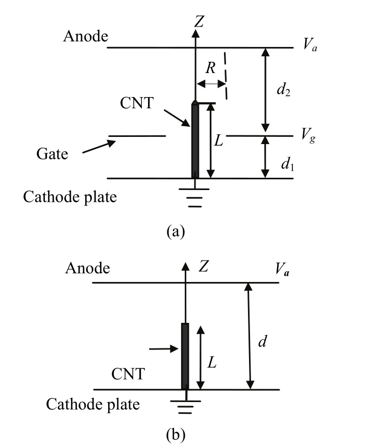
Fig. 1. Two kinds of structural models: (a) triode-structure, the distances d1= 30 µm, d2= 100 µm, and the gate hole radius is expressed by R and (b) diode-structure, the distance between cathode and anode d = 130 µm.
3. Numerical Simulation and Results Analysis
3.1 Potential Distribution
Fig. 2 shows the potential distributions simulated by using the finite element method (ignored the edge effect), near the top of the CNT in the two structures.
The significant difference in the distributions can be found: the equipotential lines in the path of electron beam in the triode-structure are parallel as shown in the dotted box of Fig. 2 (a), so the electric field in the path is uniform electric field, the electron beam is columnar as shown in Fig. 2 (c), the electrons reach vertically the anode, and its luminous efficiency then is increased. But the equipotential lines in the path of electron beam in the diodestructure are not parallel and change steeply near the top of the CNT, as shown in the dotted box of Fig. 2 (b), so the electric field is not uniform one, consequently, it is not in a vertical path for the electrons to reach the anode, so its luminous efficiency is lower naturally.
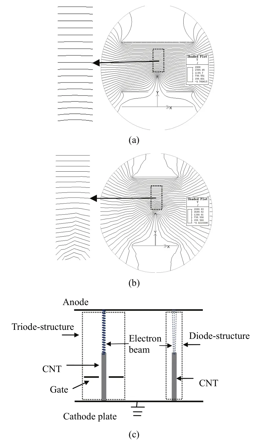
Fig. 2. Potential distribution and shape of electron beam: (a) the potential distribution in the triode-structure under anode voltage of 2000 V and gate voltage of 100 V, (b) the potential distribution in the diode-structure under the same anode voltage, and (c) shape of electron beam.
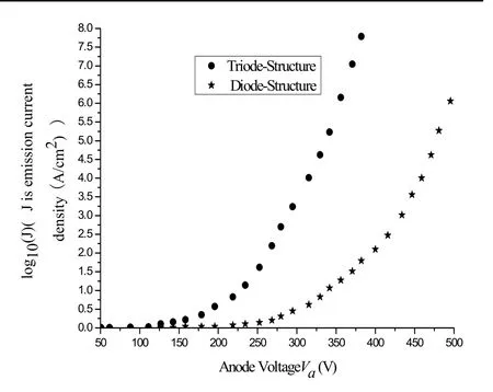
Fig. 3. Emission current density J, as a function of anode Va.
3.2 Emission Current Density
The emission current densityJof a CNT can be expressed by the Fowler-Nordheim equation as follows:

whereφ=5 eV is the work function of the CNT,Eis excitation electric field,andThe emission current densities of the two structures derived from this formula, as a function of anode voltage, are shown in Fig. 3. We can see from this figure that the turn-on voltage of the triode-structure is only 125 V, which has been decreased by 100 V compared with the diode-structure, and after turning on, the variance ratio of theJof triode-structure is much larger than that of the diode-structure. Therefore, the emission current density and turn-on voltage in the triode-structure can be adjusted by changing the gate voltage.
3.3 Excitation Electric Field and Field Enhancement Factor
The effects of the gate voltage on the excitation electric field strengthEand the field enhancement factorβare shown in Fig. 4. For the triode-structure, it can be seen from Fig. 4 (a) that 1)Ereaches its strongest at the top of the CNT, then decreases rapidly, and hereafter slowly tends to a stable value (or zero) with increasing ofr, e.g.,Ewill reduce to one tenth of its value at the top whenris equal to 10 times of the diameter of the CNT; 2) the gate voltageVgdoes not change the law thatEvaries withr, but the curve of the law rises integrally with the increasing ofVg, which means thatEwill strengthen with increasing ofVg; 3) themaximum ofEin the triode-structure is much larger than that of the diode-structure, and the tendency of theEvarying withris more steep than that of the later. So the excitation electric fieldEcan be easily changed by the gate voltageVg.
The field enhancement factorβin the triode-structure, as a function of gate voltageVg, is shown in Fig. 4 (b). It is evident that the gate voltage has a significant effect onβwhich rises with increasing of the gate voltageVg. This conclusion is consistent with the experimental results of [17] and [18]. This is because that the local electric field near the top is enhanced with increasing of the gate voltage, and more electrons are drawn to the top of the CNT. This gives rise to an enhancement in the excitation electric field further, e.g.,βcan reaches 1 in the triode-structure whenVg= 130 V,Va= 2000 V, but in the diode-structureVa= 5000 V for the identical value ofβ[19]. Soβcan be conveniently changed byVg.
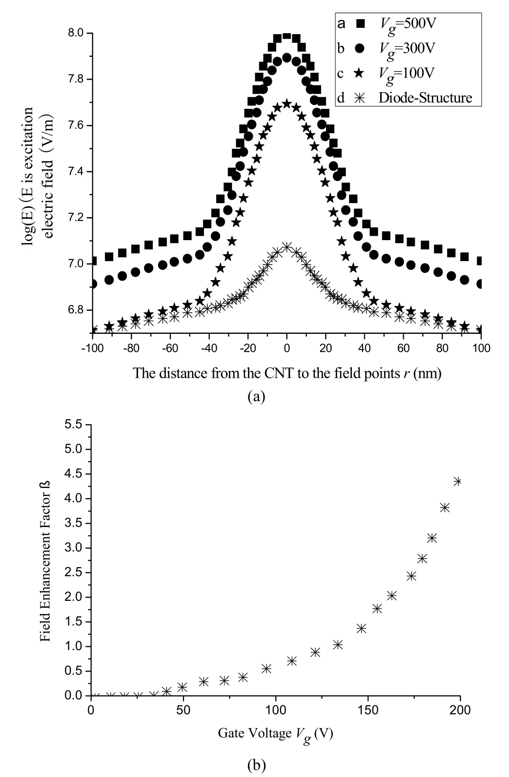
Fig. 4. Effects of gate voltage on excitation electric field E and field enhancement factor β: (a) the gate voltage dependence of excitation electric field E in the two structures. The distance from the top of the CNT to the field points is denoted by r; the axis of the CNT is defined as Z-axis and the cathode plane is defined as XOY-plane, and (b) field enhancement factor β, as a function of the gate voltage Vg.
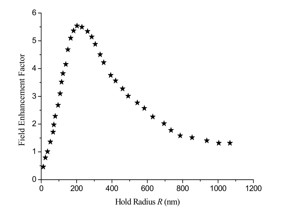
Fig. 5. Field enhancement factor β, as a function of the hole radius.
3.4 Effect of Hole Radius on Field Enhancement Factorβ
The field enhancement factorβas a function of gate hole radiusRis shown in Fig. 5. It can be seen that 1)βreaches the maximum value whenRequals 200 nm, this hole radius is 10 times of the diameter of the CNT. This conclusion agrees with the experimental results reported in [19] and [20]; 2) the effect ofRon theβoccurs within the range from 10 nm to 900 nm,βrises rapidly and up to the maximum within the range from 10 nm to 200 nm, then declines and tends to a stable value (R>1000 nm). The reason is that gate exerts a shielding effect on the top of the CNT-CC as the hole radiusRis smaller; the smaller the hole radius is, the greater the shielding effect will be. But, beyond the shielding range, the larger theRis, the larger the distance between the top and the gate will be and the smaller the enhancement will be. A similar conclusion had been reported in [21]. When the hole radius is large enough (R>1000 nm) the triode-structure is equivalent to diodestructure.
4. Conclusions
The field emission properties of the triode-structure are obviously better than the diode-structure and its adjustability of field emission properties is clearly improved due to the role of gate. Changing gate voltage properly is an effective way to adjust the field emission properties. The hole radius dependence of the field enhancement factorβcould contribute to the optimizing design of nano-cathode devices, and the recommended optimal hole radius may be 10 times the diameter of the CNT.
[1] W. A. de Heer, A. Châtelain, and D. Ugarte, “A carbon nanotube field-emission electron source,” Science, vol. 270, no. 5239, pp. 1179-1180, Nov. 1995.
[2] H. Suga, H. Abe, M. Tanaka, T. Shimizu, T. Ohno, and Y. Nishioka, “Stable multiwalled carbon nanotube electronemitter operating in low vacuum,” Surf. Interfance Anal., vol. 38, no. 12-13, pp. 1763-1767, 2006.
[3] L. Zhang, L. Balzano, and D. E. Resasco, “Single-walled carbon nanotubes of controlled diameter and bundle size and their field emission properties,” J. Phys. Chem. B, vol. 109, no. 30, pp. 14375-14381, 2005.
[4] Y. Z. Liu, Electron Emission and Photocathode, 1st ed. Beijing: Press of Beijing Institute of Technology, 1995, ch. 2, pp. 48-49.
[5] L. Song, S. Liu, G.-M. Zhang, et al., “Electron field emission from single-walled carbon nanotube nonwoven,”Chin. Phy., vol. 15, no. 2, pp. 422-427, 2006.
[6] G. Zhou and W.-H. Duan, “Template assisted synthesis of semiconductor nanowires,” Nano-Science and Nano-Technology, vol. 5, no. 5, pp. 1421-1423, 2005.
[7] C.-L. Cheng, Y.-F. Chen, R.-S. Chen, and Y.-S. Huang,“Raman scattering and field-emission properties of RuO nanorods,” Appl. Phys. Lett., vol. 86, no. 10, pp. 1407-1409, 2005.
[8] H. Jo, D. Banerjee, and Z. F. Ren, “Field emission of zinc oxide nanowires grown on carbon cloth,” Appl. Phys. Lett., vol. 85, no. 8, pp. 1407-1409, 2004.
[9] J.-C. She, S.-Z. Deng, N.-S. Xu, et al., “Fabrication of vertically aligned Si nanowires and their application in a gated field emission device,” Appl. Phys. Lett., vol. 88, no. 1, pp. 013112-013114, 2006.
[10] R.-S. Chen, Y.-S. Huang, Y.-M. Liang, et al., “Field emission from vertically aligned conductive IrO2 nanorods,”Appl. Phys. Lett., vol. 84, no. 9, pp. 1552-1554, 2004.
[11] S. Y. Li, P. Lin, C. Y. Lee, et al., “Effect of Sn dopant on the properties of ZnO nanowires,” Appl. Phys., vol. 37, no. 16, pp. 2274-2277, 2004.
[12] P. Minh, L. Tuyen, T. Ono, H. Miyashita, Y. Suzuki, H. Mimura, and M. Esashi, “Selective growth of carbon nanotubes on Si microfabricated tips and application for electron field emitters,” J. Vac Sci & Tech. B, vol. 21, no. 4, pp. 1705-1709, 2003.
[13] V. Filip, D. Nicolaescu, M. Tanemura, and F. Okuyama,“Modeling the electron field emission from carbon nanotube films,” Ultramicroscopy, vol. 89, no. 1-3, pp. 39-49, 2001.
[14] X.-Q. Wang, M. Wang, H.-L. Ge, Q. Chen, and Y.-B. Xu,“Modeling and simulation for the field emission of carbon nanotubes array,” Physica E, vol. 30, no. 1-2, pp. 101-106, 2005.
[15] Q.-H. Wang, M. Yan, and R. P. H. Chang, “Flat panel display prototype using gated carbon nanotube field emitters,” Appl. Phys. Lett., vol. 78, no. 9, pp. 1294-1296, 2001.
[16] Y. Qin, M. Hu, H. Li, et al., “Preparation and field emission properties of carbon nanotubes cold cathode using melting Ag nano-particles as binder,” Appl. Surf. Sci., vol. 253, no. 8, pp. 4021-4024, 2007.
[17] J. Kim, K. No, and C. J. Lee, “Growth and field emission of carbon nanotubes on electroplated Ni catalyst coated on glass substrates,” J. Appl. Phys., vol. 90, no. 5, pp. 2591-2596, 2001.
[18] D.-S. Chung, S. H. Park, H. W. Lee, et al., “Carbon nanotube electron emitters with a gated structure using backside exposure processes,” Appl. Phys. Lett.,” vol. 80, no. 21, pp. 1802-1805, 2002.
[19] J.-M. Bonard, N. Weiss, H. Kind, T. Stöckli, L. Forró, and K. Kern, “Tuning the field emission properties of patterned carbon nanotube films,” Adv. Mater., vol. 13, no. 2, pp. 184-188, 2001.
[20] S. Fujii, S.-I. Honda, H. Machida, et al., “Efficient field emission from an individual aligned carbon nanotube bundle enhanced by edge effect,” Appl. Phys. Lett., vol. 90, no. 15, pp. 1063-1065, Apr. 2007.
[21] Y.-K. Li, S.-L. Cheng, X.-H. Liu, et al., “Electrical numerical simulation of field emission for carbon nanotube cathode,” Journal of Liaoning University, no. 2, pp. 168-171, 2006.

Yong-Qing Guowas born in Gansu, China in 1957. He graduated from Peking University, Beijing in 1979, and received the M.S. degree from the School of Science, Lanzhou University of Technology, Lanzhou in 2008. He is currently a professor of theoretical condensed matter physics with the Institute of Modern Physics, Gansu Normal University for Nationalities. His main areas of research include nano-materials, solid state theory, and quantum field theory.

Wei-Min Zhengwas born in Gansu, China in 1977. He received the B.S. degree in 2001 and the M.S. degree from the Physics Department, Qinghai Normal University, Xining in 2004. He is now an associate professor with the Institute of Electrical and Electronic Technology, Gansu Normal University for Nationalities. His main areas of research include electrical and electronic technology, and quantum dynamics.

Xiao-Juan Zhangwas born in Gansu, China in 1979. He received the B.S. degree in 2004 and the M.S. degree from the School of Physics, Northwest Normal University, Lanzhou in 2011. He is now an associate professor with the Institute of Theoretical Physics, Northwest Normal University, Lanzhou. His main areas of research include physics of interacting many particle systems, nano-materials, and quantum dynamics.
Manuscript received October 2, 2013; revised January 25, 2014.
Y.-Q. Guo is with the Department of Physics and Hydropower Engineering, Gansu Normal University for Nationalities, Hezuo 747000, China (Corresponding author e-mail: guoyq57@163.com).
W.-M. Zheng is with the Department of Physics and Hydropower Engineering, Gansu Normal University for Nationalities, Hezuo 747000, China (e-mail: zhengwmlx@sina.cn).
X.-J. Zhang is with the School of Physics, Northwest Normal University, Lanzhou 730050, China (e-mail: zhangxjtx@163.com).
Digital Object Identifier: 10.3969/j.issn.1674-862X.2014.03.016
 Journal of Electronic Science and Technology2014年3期
- Journal of Electronic Science and Technology的其它文章
- Guest Editorial Special Section on Energy-Efficient Technologies
- Guest Editorial TTA Special Section on Terahertz Materials and Devices
- Object Tracking Using a Particle Filter with SURF Feature
- Numerical Solution for Fractional Partial Differential Equation with Bernstein Polynomials
- A High Efficiency Fully Integrated OOK Transmitter for WBAN
- Detecting Circles Using a Two-Stage Approach
