A High Efficiency Fully Integrated OOK Transmitter for WBAN
Mousa Yousefi, Ziaddin Daie Koozehkanani, Jafar Sobhi, and Hamid Jangi
A High Efficiency Fully Integrated OOK Transmitter for WBAN
Mousa Yousefi, Ziaddin Daie Koozehkanani, Jafar Sobhi, and Hamid Jangi
—A 2.4 GHz high efficiency radio frequency (RF) transmitter for wireless body area network (WBAN) in medical applications is presented in this paper.The transmitter architecture with high energy efficiency is proposed to achieve a high data rate with low power consumption. In conventional transmitters, the oscillator and power amplifier are turned off when the transmitter sends 0. The required time for turning oscillator ON/OFF is longer than the other blocks of the transmitter. In the proposed transmitter, the low power oscillator is on all the time while the power amplifier and modulator are turned off when “0” data is sent. The transmitter consumes 3.2 mW at 0.5 dBm output by 285 Mbps data rate and the energy consumption per transmitted bit with 0.5 dBm output power is 10 pJ/(bit·mW). The proposed transmitter was designed in 0.18 µm CMOS technology.
Index Terms—On-off keying, power amplifier, transmitter, wireless body area network.
1. Introduction
Wireless body sensor network provides wireless connectivity among sensors that are used for exhibition vital signals of body and personal services. Vital signal monitoring, diagnose assistant, and drug delivery are medical applications of wireless body area network (WBAN)[1],[2]. Personal computer, cell phone, wireless local area network (WLAN), and internet network for personal services are used to connect with medical center and WBAN. Fig. 1 shows a typical scenario of WBAN applications.
In typical WBAN applications, the distance between a sensor node and the gateway node is less than 3 m. The output power for transmitter is less than 1 mW. The sensor node is composed of sensing section, analog to digital converter (ADC), digital processor, and transceiver. The sensor node must be small to limit the required source energy. Since the transceiver is a block with high power consumption, as a result, the design of a radio frequency (RF) transceiver is a challenge for the WBSN sensor node.
In most reported papers, the figure of merit for transmitter was that how much energy is consumed for sending one bit by assuming that error did not occur in data transmission. Conventional figure of merit (FOM) does not take the transmission power into account. Transmitters that have a high output power normally consume more DC power, which is a disadvantage. Through this work, an alternative FOM is used, denoted FOMTX, which normalizes the energy efficiency to the output power,Po. That is,

FOMTXhas been used as a better FOM to compare different transmitters[3],[4]. The high data rate wireless connection is required for applications like capsule endoscopy or multichannel biosensor recording. In order to maximize the life time, data rate must be kept high while DC power is kept low. ON/OFF keying (OOK) and frequency shift keying (FSK) are dominant modulation methods in the RF transceiver of the sensor node.
A transmitter architecture with high energy efficiency is proposed in this paper to achieve high data rate with low power consumption. This paper is organized as follows: Section 2 describes the basic operation of the transmitter. Simulation results are presented in Section 3. Finally, Section 4 concludes the paper.
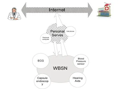
Fig. 1. Typical scenario of WBSN applications.
2. Transmitter Structure
The transmitter (TX) block diagram is shown in Fig. 2. In this design, the OOK modulation scheme is utilized, in which binary “1” is represented by a pulse and binary “0”by no pulse transmission. The TX adopts a simple circuitry structure to save power. It is composed of two major building blocks: the oscillator and the power amplifier (PA). The OOK TX can be easily realized by turning on or off the PA according to message data. But, the oscillator is on all the time to increase data rate. So for designing of low power TX, the oscillator must be low power.
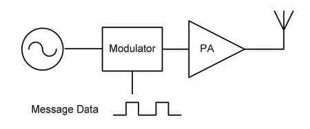
Fig. 2. Block diagram of transmitter.
2.1 Oscillator
Oscillators are blocks that play a key role in wireless communication networks. In conventional high data rate OOK transmitters, oscillators and power amplifiers turn off when the transmitter sends “0” data. However, all of components of the transmitter must be switched on and off with data rate frequency. The required time of ON/OFF duration of all the blocks determines the maximum data rate frequency. The required time for ON/OFF duration of oscillator is higher than the other blocks of TX. Because the oscillator switching is time consuming, in the proposed transmitter, the oscillator is on all the time.
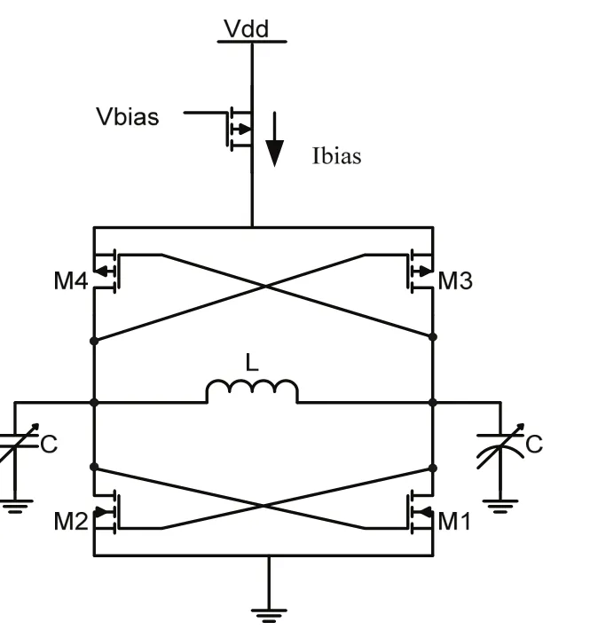
Fig. 3. Complementary oscillator.
In the proposed TX, the LC complementary oscillator used with its circuitry is shown in Fig. 3. It generates the digital signal to control the capacitance of the LC tank, which is composed of a C bank with 4 transistor switches and generates sixteen overlapped discrete tuning curves to increase the desired frequency tuning range. A voltage controlled variable capacitor is used for fine calibration. The resonation frequency of the oscillator can be controlled by tuning the C bank. Simulation results show that the tuning range is about 2.01 GHz to 2.346 GHz with a 21 MHz/LSB.
The amplitude voltageVampis proportional to the parallel resistance and bias current:

whereRpis the equivalent resistance which is determined by the quality factor of inductor.
In the complementary oscillator, high swing voltage requires high bias current or parallel resistance. However, high bias current will increase power consumption and large parallel resistance requires highQinductor. Unfortunately, the integrated inductor inherently has low quality factor andRpcould not be high. Since the oscillator must have enough output voltage swing for driving an inverter gate, the DC current must be increased.
In the designed complementary oscillator, the bias current is 1 mA and the inductor of 4.5 nH hasQequal to 6.5. The output voltage swing is 0.4 V that is sufficient for driving a modulator. Table 1 summarizes the simulation results for different on-chip spiral inductors. In the designing TX, we have used an inductor of 4.5 nH with 336 MHz tuning range with 21 MHz/LSB. The designed oscillator has -117 dBc/Hz (1 MHz offset) frequency phase noise and 0.4 V output swing.
For the design of ultra low power oscillators, higherQinductors can be used, which in turn results in an increased area.
2.2 PowerAmplifier
The class-E PA (power amplifier) fully integrated circuit architecture has been used. The class-E PA which can ideally achieve 100% efficiency is a nonlinear switching type power amplifier[5],[6]. High efficiency is the key in designing a low power transmitter PA. Many researches for high efficiency power amplifier have been done.
The class-E PA reported in [7] achieves 55% efficiency. Fig. 4 shows the class-E power amplifier employed in the transmitter. All inductors are on-chip spiral inductors. The inductor L3is chosen as DC feed. The capacitor C2provides alternative current path for higher harmonics. The inductor L3and the capacitor C3form an impedance matching network which transforms the antenna resistance toReqat the desired output frequency (ωo). The inductor L4also helps attenuating higher harmonics current components.

Table 1: Simulation results for designed LC oscillator
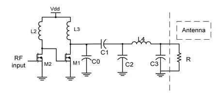
Fig. 4. Schematic diagram of power amplifier.
Unlike conventional structures, harmonic rejection is now provided by both L4and C3. This allows smaller L4to be chosen for on-chip implementation. It should be pointed out that the proposed architecture has merged the harmonic rejection and impedance matching into a π-network consisting of L4, C2, and C3. For this architecture, the drain parasitic capacitance of switching transistor can be incorporated into C0, whereas the pad parasitic parasitism can be merged with C3. Therefore, the circuit shown in Fig. 4 can be a compact representation of the actual implemented PA with all parasitic taken into account.
This circuit is designed to operate with a 0.5 V supply and 0.5 dBm output power. By changing power supply, the output power can be changed. With this characteristic of PA, the transmitter will be capable of saving energy.
2.3 Modulator
The circuitry of modulator is shown in Fig. 5. The modulator is used to modulate carrier signal with message data. The switching of transmitter is carried out by the modulator. As demonstrated in Fig. 5, the modulator is composed of 3 inverters with a switching transistor Msw. When the transmitter sends “0” message data, Mswtransistor turns on and sending “1” data turns off. Also, the other functions of modulator are driving the power amplifier and isolating antenna from the oscillator. In other words, the modulator turns the transmitter ON/OFF. The required power supply for modulator is 1 V.
In this proposed design, the data rate of the transmitter is determined by the rise and fall time of PA or modulator. The results show that the rise time and fall time of transmitter is less than 1.5 ns.
To drive the modulator properly, the DC operating point and output amplitude of the oscillator both are important. Simulation results show that minimum values of DC point and amplitude of input modulator are 310 mV and 280 mV, respectively. Also, at the maximum DC point of 400 mV, the output amplitude is 510 mV. With these conditions, as a result, the oscillator should have the oscillation with the minimum 310 mV amplitude and the DC point of output can change between 310 mV and 520 mV.
Tuning frequency with the array capacitance bank and the variation of power supply can alter the DC point and amplitude of output. With turning on and off all of switches, the output amplitude of output varies between 420 mV and 445 mV, and the DC point of output changes between 419 mV and 443 mV. The modulator works reliably over whole this range of variations.
2.4CircuitDesign
The prototype of the transmitter was designed in the 0.18 µm CMOS process. The schematic of the transmitter is shown in Fig. 5. In this design, the data rate is limited by the startup time of the power amplifier, not the oscillator. The comparison table shows that FOM for the proposed circuit is better than other techniques (see Table 2).
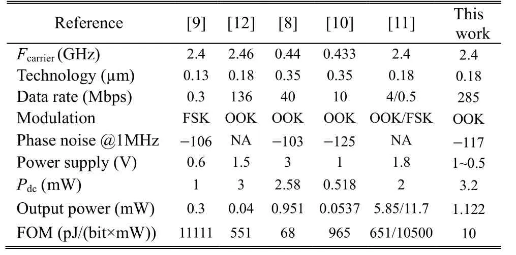
Table 2: Performance comparison of TXs
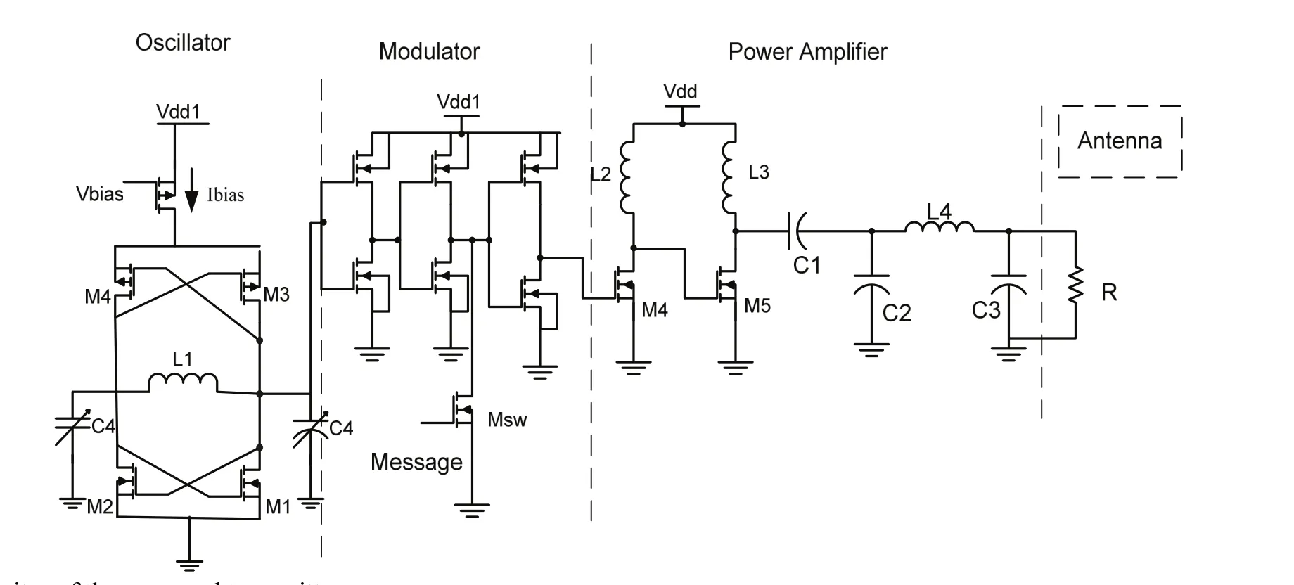
Fig. 5. Circuitry of the proposed transmitter.
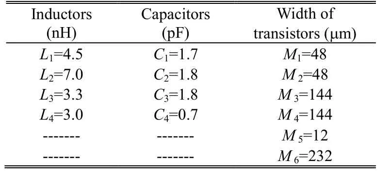
Table 3: Device sizing for proposed transmitter
In the overall circuit, all transistors are in 0.18 μm CMOS technology. The width of transistors and the value of other elements of the transmitter are shown in Table 3. The output matching network consists of inductor L4(3.3 nH) and capacitors C3(2 pF). The L2(3.3 nH) and L3(3 nH) are realized via spiral on-chip inductors.
3. Results
The proposed transmitter has designed on a 0.18 µm CMOS process and the proposed TX characteristics are listed in Table 4. The oscillator has a 2.4 GHz output signal with the minimum 0.4 V output swing. In Fig. 6, the output modulated signal waveform is shown with “1010” data message and 285 Mbps data rate. The oscillator consumes 1.2 mA from 1 V power supply. Fig. 7 shows the DC point and output amplitude of the oscillator versus power supply. Fig. 8 shows the layout of the proposed transmitter which has 1.2 mm × 1.2 mm area excluding the pads. Fig. 9 shows the phase noise of the transmitter output. The phase noise is less than -117 dBc/Hz beyond 1 MHz offset.
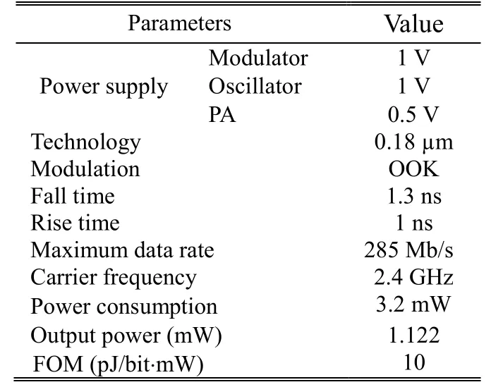
Table 4: Summary of characteristic of the proposed TX
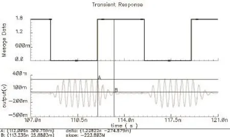
Fig. 6. Waveform of output modulated signal with "1010" data message and 285 Mbps data rate.
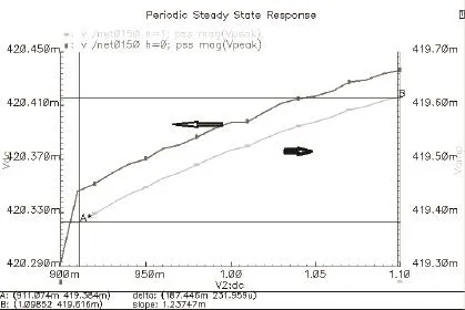
Fig. 7. DC point and output amplitude of the oscillator versus power supply.

Fig. 8. Layout of the TX.
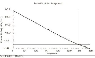
Fig. 9. Phase noise of transmitter.
The output power of the transmitter is 0.5 dBm at 50 Ω load. The performance comparison with other low power transmitters is shown in Table 2. The FOM of the proposed transmitter is 10 pJ/(bit×mw). The designed transmitter performs favorable compared with other reported transmitters.
4. Conclusions
A highly efficient OOK transmitter has proposed for wireless body sensor networks. The transmitter chip has been designed in 0.18 μm CMOS process. The oscillator and class-E power amplifier compose an OOK transmitter with 285 Mbps data rate and 10 pJ/(bit×mW) FOM. Theproposed transmitter requires two different supply voltages, where the PA uses 0.5 V while the modulator block and oscillator work under 1 V power supply. In this design, the data rate is limited by the startup time of the power amplifier, not the oscillator. Also, the low power oscillator is on all the time. The proposed high efficiency transmitter is well suited for high data rate monitoring of biomedical signals.
[1] A. W. Wong, D. McDonagh, G. Kathiresan, et al., “A 1V micropower system-onchip for vital-sign monitoring in wireless body sensor networks,” in Proc. of IEEE Int. Solid-State Circuits Conf., San Francisco, 2008, pp. 138-139.
[2] Y.-J. Yang, Y.-J. Huang, H.-H. Liao, et al., “A release-on-demand wireless CMOS drug delivery soc based on electro thermal activation technique,” in Proc. of IEEE Int. Solid-State Circuits Conf., San Francisco, 2009, pp. 288-289.
[3] M. Vidojkovic, X. Huang, P. Harpe, et al., “A 2.4 GHz ULP OOK single-chip transceiver for healthcare applications,” in Proc. of IEEE Int. Solid-State Circuits Conf., San Francisco, 2011, pp. 458-460.
[4] B. Otis, Y. H. Chee, and J. Rabaey, “A 400 μ W-RX 1.6 m W-TX super-regenerative transceiver for wireless sensor networks,” in Proc. of IEEE Int. Solid-State Circuits Conf., San Francisco, 2005, pp. 396-606.
[5] N. O. Sokal, “Class-E RF power amplifiers,” QEX Commun. Quart, vol. 204, pp. 9-20, Jan./Feb. 2001
[6] F. H. Raab, P. Asbeck, S. Cripps, et al., “RF and microwave power amplifier and transmitter technologies,” High Freq. Electron., vol. 2, no. 3, pp. 22-36, Jul. 2003.
[7] J. Tan, C.-H. Heng, and Y. Lian, “Design of efficient class-E power amplifiers for short-distance communications,” IEEE Trans. on Circuits and Systems I: Regular Papers, vol. 59, pp. 2210-2220, Oct. 2012.
[8] D. C. Daly and A. P. Chandrakasan, “An energy-efficient OOK transceiver for wireless sensor networks,” IEEE J. Solid-State Circuits, vol. 42, no. 5, pp. 1003-1011, May 2007.
[9] B. W. Cook, A. D. Berny, A Molnar, et al., “An ultra low power 2.4 GHz RF transceiver for wireless sensor network in 0.13 µm CMOS with 400 mw supply and an integrated passive RX front-end,” in Proc. of IEEE Int. Solid-State Circuits Conf., San Francisco, 2006, pp. 1460-1469.
[10] M. K. Raja and Y.-P. Xu, “A 52 pJ/bit OOK transmitter with adaptable data rate,” in Proc. of IEEE Asian Solid-State Circuits Conf., Fukuoka, 2008, pp. 341-344.
[11] Q. Zhang, X.-F. Kuang, and N.-J. Wu, “An ultra-low-power RF transceiver for WBANs in medical applications,” Journal of Semiconductors, vol. 32, no. 6, pp. 065008-1-065008-8, 2011.
[12] J. Jung, S. Zhu, P. Liu, and Y.-J. Chen, “22-pJ/bit energyefficient 2.4-GHz implantable OOK transmitter for wireless biotelemetry systems: In vitro experiments using rat skin-mimic,” IEEE Trans. on Microwave Theory and Techniques, vol. 58, no. 12, pp. 4102-4111, 2010.

Mousa Yousefireceived the B.S. degree from University of Urmia, Iran and the M.S. degree from Tabriz University, Iran, both in electrical engineering. His research interests are data converter design, mixed signal circuits design, and RF integrated circuits. He is currently a Ph.D. student with the Faculty of Electrical and Computer Engineering, University of Tabriz, Tabriz, Iran.

Ziaddin Daie Koozehkananireceived his Ph.D. degree in electrical engineering from the Brunel University of West London, UK in 1996. He has been teaching as an assistant professor in Urmia University from 1996 to 2004 and in University of Tabriz since 2004. At the time he worked as an associated professor with the Faculty of Electrical and Computer Engineering, University of Tabriz, he served as the Dean of the faculty. His current scientific interests are analog integrated circuit design including data converters, RF IC design, and optical filter design.

Jafar Sobhiwas born in Tabriz, Iran. He received B.S. degree in electrical engineering from University of Tabriz, Iran. He received M.Sc. and Ph.D. degrees in electrical engineering from Urmia University. His research interests are high-speed high-resolution data converter design, mixed signal circuits design, and RF integrated circuits design. He is currently with the Faculty of Electrical and Computer Engineering, University of Tabriz, Tabriz, Iran.

Hamid Jangireceived B.S. degree from Iran University of Science and Technology in 2000 and the M.S. degree from Sharif University in Tehran, Iran in 2008, both in electrical engineering. He is currently a Ph.D. student with the Faculty of Electrical and Computer Engineering, University of Tabriz, Tabriz, Iran.
Manuscript received August 22, 2013; revised March 12, 2014.
M. Yousefi is with the Faculty of Electrical and Computer Engineering, University of Tabriz, Tabriz 51666-158, Iran (Corresponding author e-mail: m.yousefi@tabrizu.ac.ir).
Z. D. Koozehkanani, J. Sobhi, and H. Jangi are with the Faculty of Electrical and Computer Engineering, University of Tabriz, Tabriz 51666-158, Iran (e-mail: zdaei@tabrizu.ac.ir; sobhi@tabrizu.ac.ir; hamid.jangi@yahoo.com).
Digital Object Identifier: 10.3969/j.issn.1674-862X.2014.03.015
 Journal of Electronic Science and Technology2014年3期
- Journal of Electronic Science and Technology的其它文章
- Guest Editorial Special Section on Energy-Efficient Technologies
- Guest Editorial TTA Special Section on Terahertz Materials and Devices
- Object Tracking Using a Particle Filter with SURF Feature
- Numerical Solution for Fractional Partial Differential Equation with Bernstein Polynomials
- Role of Gate in Triode-Structure for Carbon Nanotube Cold Cathode
- Detecting Circles Using a Two-Stage Approach
