Characteristics of a Surface-Breakdown Triggered Vacuum Switch with Six-Gap Rod Electrode System
2012-06-06 16:15:10
电工技术学报 2012年10期
(State Key Laboratory of Advanced Electromagnetic Engineering and Techno logy Huazhong University of Science and Technology Wuhan 430074 China)
1 Introduction
Triggered vacuum switch(TVS) is developed based on the technology of vacuum gap and triggered spark gap.It has been applied widely in the field of high pulsed power system,due to the merits of wide operating voltage range,high current capability,high transfer charge,flexible trigger system,high trigger reliability,rapid dielectric recovery,long life,low noise,etc[1-3].
The research on TVS began in 1960s.Lafferty did an abundant work on the TVS with flat-type electrode system[4].However,the flat-type electrode system has its own shortcomings,such as vacuum arc concentration,limiting the development of greater current carrying ability.So the GE Company proposed a kind of six-gap rod electrode system,i.e.,the main electrodes of switch are made up of multi-rod electrodes,the rod electrodes cross each other and are arranged in a circle,forming parallel vacuum gaps[5-7].In these electrode systems,the vacuum arc will keep diffusion and avoid the serious erosion of the electrodes.So,it is helpful to improve the current carrying ability and the long life of electrodes.However,the research focus of switch for GE Company was changed to the SF6insulation,so TVS with rod electrode system developed no more.While the All-Russian Electrotechnical Institute improved this kind of TVS continually and developed a series of TVSs with six-gap rod electrode system,such as RVU-40,RVU-43,RVU-45 and RVU-47[8,9].
In this paper,a surface-breakdown TVS sample with six-gap rod electrode system was fabricated,which has less trigger delay and trigger burden due to the special surface-breakdown trigger pin structure.The main operating characteristics are proposed and the working polarities are discussed.
2 TVS construction
The construction of surface-breakdown TVS with six-gap rod electrode system is shown as Fig.1,with height of 155mm,diameter of 113mm and mass of 4kg.It is mainly made up of an insulated ceramic shell,a metal shield,a pair of main electrodes with rods,and a trigger pin.The shell keeps the inner vacuum degree at 1.33×10⁻⁴Pa commonly,and isolates the main electrodes.Metal shield can adjust the distribution of electric field in TVS,and protects the inner surface of the shell,keeping metal vapor away from the inner surface,which will reduce its dielectric strength.Main electrodes of anode and cathode each have three rod electrodes,which are positioned alternatively,transmitting the heavy current.The electrode material is oxygen-free copper.The trigger pin is set in the center of the cathode through a ceramic ring whose surface is the insulation between the trigger pin and the cathode.The initial plasmas are generated through the ceramic ring surface,so it is a kind of surface-breakdown TVS.

Fig.1 Construction of TVS and its sample
The switching-on process of TVS includes two primary parts,i.e.,trigger and main gap breakdown[4].Trigger process supplies initial plasmas for the main gap.As surface-breakdown TVS,initial plasmas come from the ceramic surface collapse and its needed time is called wait time.With the help of main electric field,the initial plasmas enter the main gap and cause the breakdown of main gap,leading to the burning of metal arc.The needed time of this process is called collapse time.When the arc current crosses the zero,the TVS is switched-off.
3 Test platform
A test platform was set up as Fig.2.It includes the loop 1 of high voltage low current and the loop 2 of low voltage high current,shown as the left part and the right part of the Fig.2,respectively.T1and T2are step-up transformers,K1and K2are disconnecting links,and Tr is the trigger system of the TVS.The other detailed parameters are shown in Tab.1.

Fig.2 The test platform

Tab.1 Parameters of the test platform
When K1is closed and K2is open,the TVS works in the loop 1.The capacitor ofC1will discharge throughR,K1and the TVS.It is easy to obtain the operating parameters,such as working voltage,trigger reliability,delay,working polarities,etc.
When K1is open and K2is closed,the TVS works in the loop 2.The capacitor ofC2will discharge throughL,K2and the TVS.From loop 2,the high current is obtained,so do the dielectric recovery,arc voltage,trigger life,electrode life,etc.
The detailed schematic of TVS trigger system is shown as Fig.3.T3is the step-up transformer,while T4is the pulse transformer.When the SCR (siliconcontrolled rectifier) is closed,the capacitor ofC3will discharge through the SCR and the primary leakage reactance of T4.Diode VD4is the crowbar switch.C4is a ceramic capacitor of high-voltage connected parallel to the secondary winding of T4,which can store trigger energy and increase the trigger current.

Fig.3 Schematic of trigger system
The Pearson current monitor of model 4427 was used in the measurement of high current and the Tektronix P6015A was adopted for the high voltage.The digital storage oscilloscope was Tektronix TDS 2022B,with band width of 200MHz.
4 Results and characteristics
4.1 Operating voltagae
The self-breakdown voltage is about 30kV,and the TVS sustains such a voltage not more than 30s.However,the TVS can sustain a voltage of 25kV more than 5 minutes.The main gap is about 10mm,so the high self-breakdown voltage is due to the uniform electric field.Fig.4 is the simulation of electric field in the main gap,showing that the field difference is small,although it is larger on the surface of the rods.The uniform electric field is one of the advantages of the rod electrode system.
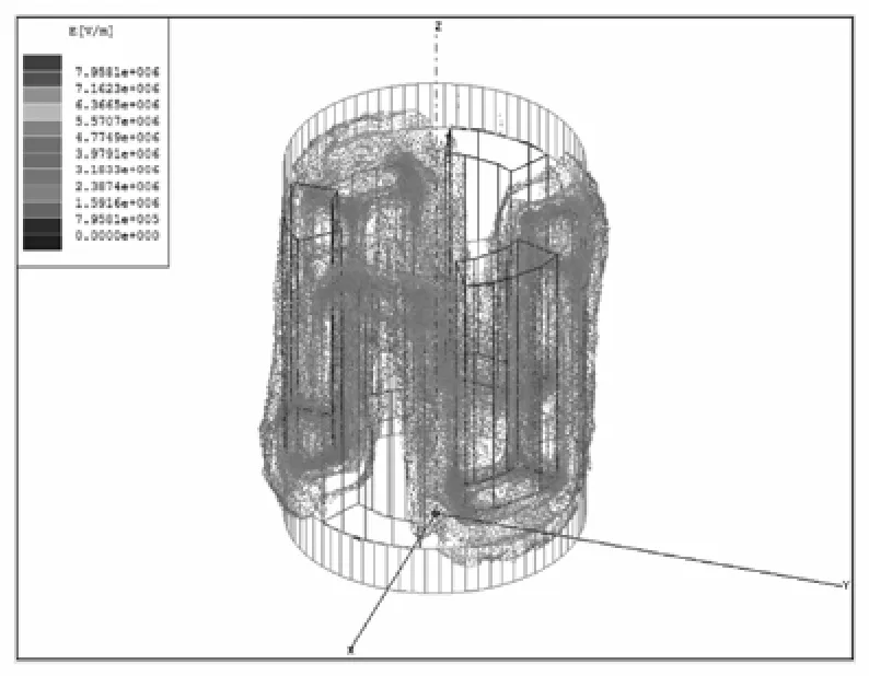
Fig.4 Uniform electric field in the main gap
Even 50V of main gap voltage,the TVS can be still switched-on.The main gap voltage and current are shown as CH1 and CH2 in the Fig.5,respectively.Although there are some noises during the collapse process of main gap,the trigger reliability is also 100% nearly.
So,the TVS sample has an operating voltage of 0.05~25kV.Especially,the lowest working voltage can reach 50V,which means the main gap voltage has little influence on the trigger reliability.
4.2 High current
The different high currents can be obtained by changing the charged voltages ofC2.For example,when theC2is charged to 1kV,2kV,3kV and 4kV,the currents of 22.8kA,47.2kA,74.4kA and 100kA are obtained,respectively.

Fig.5 Lowest working voltage
A main current of about 48kA is shown as Fig.6,i.e.,the voltage ofC2is 2kV.The measurement ratio of current to voltage is 10 000∶1.When the current crosses the first zero,it is not interrupted,leading to the arcing of next negative half wave.It fails to extinguish the arcing nearby the current zero,due to the high rate of main current.It is got that di/(dt)≤330A/μs,if the TVS can cut off the current at the zero.In such a case,the TVS can work in the loop as a diode.However,the 330A/μs is not unique,due to the randomness of dielectric recovery.Test results show that it is about 330~500A/μs and 330A/μs is the lowest limit value.Meanwhile,the change rate of reverse recovery voltage (du/dt) is about 6~10kV/μs.
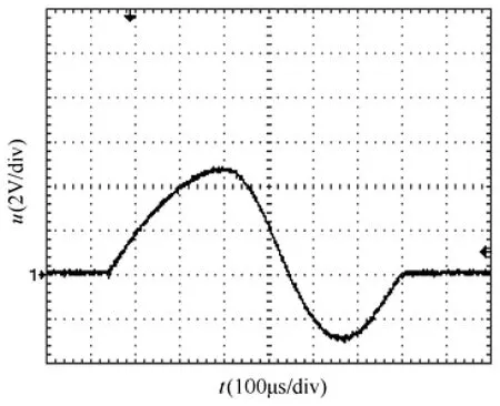
Fig.6 Failure of interrupting at the first current zero
When di/(dt) is larger than 300A/μs,which is less than the 330A/μs,due to the design margin,the diode can be connected with the TVS in series,to interrupt the current at the first zero.Peak value of 100kA is obtained,shown as Fig.7.The measurement ratio of current to voltage is also 10000:1.And the charge transferred during the high current is 26.1C.

Fig.7 Peak value of 100kA
The rated current of the TVS sample has not been reached.The slight erosion of anode and cathode can also prove this result.So,the TVS sample should have current greater than 100kA/26.1C.
4.3 Delay characteristic
According to the basic process of switching-on TVS,the TVS delay includes two primary parts,i.e.,wait timet1during the trigger process and collapse timet2during the main gap breakdown.Typical waveforms of switching-on TVS are shown in Fig.8,where CH1 is the main gap voltage collapse and CH2 is the trigger pulse.From CH2,the rise time of trigger pulse from its zero voltage to the peak value is 700ns,i.e.,t1≈700ns.From CH1,the collapse time of main gap from its charged voltage to zero is about 300ns,i.e.,t2≈300ns.

Fig.8 Waveforms of switching-on delay
It is obvious that thet1will reduce along with the trigger voltage peak lower,due to the decrease of ceramic ring surface insulation.That is because an evaporated metal film will cover the ceramic surface during the trigger and main gap arcing process.This conducting film is benefited to reduce the insulation and has relationship with the life of TVS.For the trigger voltage of 0.2~7kV,the range oft1is about 200~800ns.
Meanwhile,thet2will increase with the enhancement of charged voltage ofC1orC2.For the charged voltage ofC1during 0.5~14kV,thet2is got at 300~700ns.From the typical data,a fitting curve oft2to the main gap voltage is shown as Fig.9,showing exponential increase tendency.The mathematical expression isy=a+blnx,wherea=422.8,b=94.9.So when the main gap voltage is 24kV,the calculated result oft2is about 724ns.According to the highest working voltage of 25kV,it is considered that the 700ns may be the longest collapse time,which is also agreement with typical data of the highest three points in the Fig.9.

Fig.9 Fitting curve of collapse time
The fitting curve is different to thet2of flat-type TVS,which is negative exponential decrease with the main gap voltage[10].That is mainly due to the special electric field in the six-gap rod electrode system.From Fig.4,it is obvious that the electric field in the six-gap rod electrode system is horizontal chiefly,so it is unfavorable to the diffusion of initial plasma in the center of the cathode.The electric line of force is vertical to the primary velocity of initial plasma.So,it may be longer when the main electric field is enhanced.When the wait time adds the collapse time,the total delay of switching-on the TVS is about 0.5~1.5μs.Further more,it is shown that the collapse time has little relationship with the trigger current.When main gap voltage is 3kV and the trigger current is changed from 50A to 250A,the collapse time is 500ns steadily.The result is shown as Fig.10.It means that the trigger pin structure is benefit to trigger the TVS sample and the small trigger current needed is helpful to design flexible trigger system,reducing trigger burden.

Fig.10 Collapse time under different trigger current
4.4 Trigger lief
The TVS life is determined by the trigger life and main electrode erosion life.The six-gap rod electrode system is benefited to protect the electrode erosion due to the uniform electric field and arc diffusion.So,it is always the trigger life that indicates the TVS working life.
As mentioned in 4.3,the trigger voltage is in a range of 0.2~7kV.In other words,when the trigger voltage is too low or too high,it will be difficult to trigger the TVS steadily.The decrease of trigger voltage is due to the evaporated metal film on the surface of ceramic ring,while the increase of trigger voltage is due to the extension of the ceramic ring surface,which will be caused by the erosion of cathode connected to the ceramic ring.
The main current is 100kA,and its result of 1000 shots is shown as Fig.11.The trigger voltage is high when the TVS is new.The trigger voltage is decreased from 6kV to hundreds of volts after about 100 shots.However,it maintains tens of volts to hundreds of volts,and seems to be stable.It is a consequence of the equilibrium between the deposition on and the removal of the metal vapor from the ceramic surface.After 1000 shots of 100kA,the TVS is still in good condition.
Further work shows that the TVS can still be switched-on steadily,when the trigger voltage is under 100V.Lafferty reported a TVS of trigger voltage of 50V[4].According to the report of Farrall,the lowest trigger voltage is about 17~35V[11].The TVS proposed in this paper has a long life time,which is in accordance with the reports.

Fig.11 Trigger life of 1000 shots
4.5 Working polarities
According to the polarities of main gap and trigger pulse,there are four working modes,shown in Fig.12.The P+has been discussed in the 4.3,which means main gap voltage is positive,and so do the trigger pulse.

Fig.12 Working polarities of different modes
When P-is working,it is almost the same to P+.For example,the collapse time is also 500ns during the different trigger currents when main gap voltage is 3kV,i.e.,the trigger current has little influence on the collapse time,too.Its collapse time fitting curve is shown as Fig.13,i.e.,y=a+blnx,wherea=160.1,andb=189.9.When main gap voltage is 24kV,t2=763μs.

Fig.13 Fitting curve of collapse time of P-
However,the main gap collapse process of P-has much more noise than the P+.When a negative trigger pulse is applied to the trigger pin,the initial plasmas are generated and the primary cathode spots are set up on the top face of the trigger pin.So,when the main gap breakdown,the main cathode should set up new cathode spots of itself to conduct the arc current.During the disappearance of primary cathode spots on the top face of trigger pin and the birth of new cathode spots on the main cathode,the noise detected is unavoidable.For positive trigger pulse,the primary cathode spots are set up on the main cathode at first,which can be used to support the main arc current.So,the P+collapse waveform is smoother,meanwhile it can protect the erosion of the trigger pin.
When N+is working,the successful trigger rate is 20% only.Although the initial plasmas are generated every time,it is difficult to lead the breakdown of main gap.A typical breakdown of main gap is shown in Fig.14,where CH1 is the main gap voltage,and CH2 is the trigger current.From the beginning of trigger current,it is 4μs later that the main gap begins to collapse,although the trigger current has reached 250A,which should be enough according to the discussion of 4.3.

Fig.14 Trigger current and main gap voltage of N+
The main causation of this matter may be the main gap electric field.The initial plasmas come from the flashover of ceramic ring surface,so it is made up of electrons mostly and positive ions a little.The negative main electric field inhibits the electrons spreading into the main gap,while accelerate the positive ions.However,just a little positive ions are generated during the flashover of ceramic ring surface,maybe 10% of total charged particles,so they can not lead the breakdown of main gap steadily.Only enough positive ions will cause new cathode spots on the main cathode.Additionally,it is the positive ions that cross the main gap,whose velocities are much lower than that of electrons,so the collapse time will be much longer than the positive working mode.It is agreement with the 4μs tested in the Fig.14.Test results show that the collapse time of N+will be in a range of 4~7μs when the effective main gap voltage is 1.5~6kV.
When N-is working,the test results are almost similar to the results of N+.The only difference is the collapse time of N-may be a little smaller than N+.The causation may be the negative trigger pulse has a stretching force to the positive ions,which will make the ions have upward primary velocities,because the top face of trigger pin is upon the ceramic ring.So,the collapse time of N-is in a range of 3~4.5μs when the effective main gap voltage is 1~3kV and its successful triggered rate can reach 40%.
However,both of N+and N-are difficult to be used in the real pulsed power system,mainly due to the low trigger rate.It is not reliable in the negative working mode.On the other hand,because of the high reliability of positive working mode,the P+and P-are suggested to be used,especially the P+.
5 Conclusions
A surface-breakdown TVS with six-gap rod electrode system was fabricated,with working voltage of 0.05~25kV,current of 100kA and transferred charge in a pulse of 25C.
Due to the trigger pin structure,the total trigger delay is reduced to 1.5μs or less,including the wait time of 800ns and the collapse time of 700ns.The trigger system is flexible and trigger life is long.
Because of the different amount and movement of charged particles during the process of leading to the main gap collapse,the positive working mode is reliable and has low trigger demands,short switching-on delay.However,the negative working mode has low trigger rate and long delay.So,the positive working mode is more advantageous and is the first choice of usage.
Reference
[1] Green A J,Christopoulos J.Plasma buildup and breakdown delay in a triggered vacuum gap[J].IEEE Trans.Plasma Sci.,1979,PS-7(2): 111-115.
[2] Shang W,Damstra G C.The main gap discharge type and mechanism of a triggered vacuum gap[C].Proc.17th ISDEIV,1996: 51-55.
[3] Zhengyang Z,Xiongying D,Minfu L,et al.Plasma stability in a triggered vacuum switch[J].IEEE Transaction on Plasma Science,2009,37(4): 555-559.
[4] Lafferty J M.Triggered vacuum gaps[J].Proc.IEEE,1966,54(1): 23-32.
[5] Farrall G A.Low voltage firing characteristics of a triggered vacuum gap[J].IEEE Trans.Electron Devices,1966,ED-13(4): 432-438.
[6] Rich J A,Farrall G A,Imam I,et al.Development of a high-power vacuum interrupter[S].General Electric Company,Schenectady,NY,EPRIEL-1895,1981.
[7] Warren T,Dickens J,Neuber A,et al.Development of improved triggered vacuum switches [C].Proceeding of Pulsed Power Conference,1999,2: 1264-1267.
[8] Alferov D F,Sidorov V A.Modernized triggered vacuum discharge switch with a six-gap Electrode System[J].Instruments and Experimental Techniques,1996,39(3): 390-395.
[9] Alferov D F,Ivanov V P,Sidorov V A.High-current vacuum switching devices for power energy storages[J].IEEE Transaction on Magnetics,1999,35(1):323-327.
[10] Zhou Z,Duan X,Liao M,et al.Operational Characteristics of a field-breakdown triggered vacuum switch[J].IEEE Trans.Magn.,2009,45(1):564-567.