
A New Design Method for Variable Digital Filter Based on Field Programmable Gate Array(FPGA)
2012-02-08 06:57:34HUWenjing胡文静QIURunhe仇润鹤LIWaiyun李外云
关键词:文静
HU Wen-jing(胡文静),QIU Run-he(仇润鹤),LI Wai-yun(李外云)
1 School of Information and Communication Engineering,Hunan Institute of Science& Technology,Yueyang 414006,China
2 College of Information Science and Technology,Donghua University,Shanghai 201620,China
3 School of Information Science and Technology,East China Normal University,Shanghai 200062,China
Introduction
Digital filterhasmany applicationsin communication systems,image processing,acoustic signal processing and other fields.Because of its good features such as only zeros,linear phase,stability and design flexibility,the finite impulse response(FIR)filter is widely employed in digital signal processing(DSP).Considerable work has been done to design an FIR filter using constantcoefficients,which can only obtain fixed frequency-domain characteristics at a time.Unlike conventional digital filter,variable digital filters(VDFs)can change their filter-type,number of taps and coefficients constantly such that the desired frequency-domain characteristics can be obtained.
Previous researches had been proposed variable digital filter implementation using the partial reconfiguration,in which a given subset of internal components was partially reconfigured.The proposed FIR filter architecture is capable of operating for different word length filter coefficients without any overheads in the hardware circuitry[1].A partially self-reconfigurable adaptive FIR filter system was proposed in paper[2],in which the dynamic partial reconfiguration method and configuration memory on field programmable gate array(FPGA)were used.Nowadays,the embedded micro-processor(EMP)based on FPGA generates a special interest on this field[3-8].
In this paper,a design scheme of VDFs based on FPGA and EMP is presented,which plays both the coefficient-calculation and programmable FIR(P-FIR)filter.The design scheme accords with the design method of system on a chip(SOC).Moreover,it is possible to update the FIR algorithm and meet the need of other digital filter systems in the future.
1 System Architecture
The hardware devices for the implementation of the proposed VDF based on FPGA consists of four parts.A view of the hardware structure of the VDF is shown in Fig.1.
As shown in Fig.1,the hardware structure includes a custom embedded micro-processor(CeMP)which is the control-center of the system.The P-FIR is an FIR filter whose filter-type,coefficients and number of taps can be changed to obtain the desired frequency-domain characteristic.The coefficient-load controller reloads the coefficients from CeMP into the P-FIR.The clock-manager and analog/digital(A/D)or digital/analog(D/A)controller is adapted to manage the clock-generator of the modules in the system and control the external A/D or D/A converter.
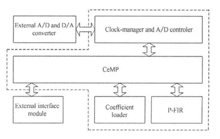
Fig.1 System architecture block diagram
The decision to adapt this kind of scheme is mainly driven by the powerful capability of computational processing,signal processing offered by the EMP implemented in FPGA.It is possible to meet the need to update the coefficient-resolving algorithm.In addition,all functions integrated on a single chip takes the advantagesofanti-interfere and reducing power consumption of the proposed system.
2 System Design
2.1 CeMP
In this work,we adapt microblaze to construct the CeMP.Microblaze is an embedded soft reduced instruction set computer(RISC)processor core with 32-bit data and address bus.The processor core is optimized for implementation in Xilinx@FPGAs,and supports both on-chip blockRAM(BRAM)and external memory[8].Meanwhile,it supports some peripherals and interface.In addition,Xilinx@provides some soft peripheral IP for this soft processor core.At the same time,according to the need of the specific application,designer can create and add their custom IP to the application system.Because of these advanced features,all the functions related coefficient-resolving,FIR and control logic can be implemented on a single FPGA.
The block diagram of CeMP is shown in Fig.2.The CeMP is composed of microblaze soft-core,BRAM,interrupt controller(IntC),Timer,DDR2/SRAM controller(MemCntlr),coefficient-load controller (CLC),and human-machine interface.The processor localbus (PLB) allows the communication and the interchange of information between microblaze and the peripherals.The local memory bus(LMB)establishes the connection of the BRAM with microblaze.CLC is a custom IP core that will be discussed in details in section 2.2.
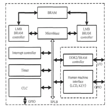
Fig.2 CeMP block diagram
We design and implement the CeMP using the Xilinx@embedded development kit(EDK)which is a part of Xilinx@integrated software environment(ISE)Suite 12.1.The Xilinx@EDK includes the xilinx platform studio(XPS),the embedded system tool suite,the embedded processing IP cores and the platform studio SDK(software development kit).For more information about Xilinx@EDK,refer to Xilinx@software manuals[9-10].
Figures 3 and 4 show the assembly view and the address map of the CeMP,respectively.As Fig.3 shows,“AddrCoef”,“DataCoef”,“Ctrl_Bits”,“LoadEn”are the interface signals between CeMP and P-FIR(will be addressed in section 2.3).“LcdData”and“LcdCtrl”are the communication ports between CeMP and the external human-machine module.
CeMP in this system performs several tasks as follows:(1)interfacing the external human-interface module to receive the user command and filter parameters;(2)resolving the FIR coefficients and filter taps;(3)writing coefficients into the coefficient register group of P-FIR filter;(4)sending the control signal to P-FIR so as to construct the desired digital filter;(5)managing the clock resource and controlling the external A/D or D/A converter and so on.
As shown in Fig.5,the coefficients and control signal are stored in the BRAM.When the filter-type and taps need to be updated,the CeMP writes the corresponding data into P-FIR under the control of signal“LoadEn”and“Write”.“CoefAddr”is the address of the coefficient register in the register group of PFIR.“DataCoef”is the values of the coefficients.“Ctrl_Bits”is the signal that is used to control the filter-type and filter taps for the P-FIR.The timing waveform of CLC is shown in Fig.6.

2.3 FPGA-based P-FIR
A P-FIR filter architecture is designed and developed as shown in Figs.7 and 8,respectively.Figure 7 shows a macro module of the programmable symmetric FIR in our system.Here,“xin”is the input sequence,“h(n)”is the tap-coefficient,“ctrl_bits”controls the order and type of FIR filter,“xout”is the shift output and“y”is the FIR output.“xout”,“xin”,and“y”can be used for cascaded FIR.

Fig.6 Timing waveform of CLC

Fig.7 FIR macro module
As shown in Fig.7,a symmetric FIR module is composed of two delay-units,two adders,one multiplier,and four multiplexers(muxes),which can be programmed as 1 or 2 taps with cascading or non-cascading under the control of“ctrl_bits”.Table 1 shows the filter taps map for the programmable module.

Table 1 Filter taps map
The FIR macro module can be used to construct higherorder FIR filter by cascading.N-order FIR filter can be obtained through cascading N/2(when N is even)or N/2+1(when N is odd)FIR macro modules.Supposing N/2 is n,when N is even,the 1st to(n-1)th macro modules are configured as 2-taps with cascading and the last macro module is configured as 2-taps without cascading.When N is odd,the 1st to nth macro modules are configured as 2-taps with cascading and the(n+1)th macro module is configured as 1-tap without cascading.
Figure 8 shows a P-FIR filter system,which can be programmed as the minimum 2 to the maximum 8 taps FIR filter operation.The“ctrl_bits”signal is 8 bits as shown in Table 2.In our system,we employ eight FIR macro module to construct minimum 1 to maximum 32 taps FIR filters.

Fig.8 Example for cascaded P-FIR

Table 2 Taps map for cascaded FIR filter
3 Experimental Results
We use Xilinx@12.1 for synthesizing purposes.The synthesis is done on Xilinx@'s virtex-5 XC5VLX110T.The whole system is implemented in the ML505 Xilinx@Development BoardthathousesanXC5VLX110T-FF1136 Virtex-5 FPGA and a systemACE module.The CeMP is clocked at 300 MHz and the peripherals run at 100 MHz.In our implementation,the filter specifications:sampling frequency fs=10 MHz,hamming window,the coefficient word-length is 16 bit fixed point format with one fractional bit,filter order N =32,input value word-length is 12 bit,FIR output word-length is 34 bit(most significant bit(MSB)truncation to 14 bit before inputted to D/A converter).The test signal is the sum of a sine wave whose frequency is 50 kHz and a linear chirp wave whose frequency is between 0.1 Hz and 3 MHz,which is converted to 12 bit digital signal through A/D converter and serves as the FIR input.
In our system,the A/D converter is ADS805 that provides 20 MHz sampling,12 bits digital output,the D/A converter is DAC5674 that provides 14 bits resolution and high speed up to 400MBPS.
The post-simulation result is shown in Figs.9-12.The proposed system in this paper can change its frequency domain characteristics to implement low pass filter(LPF),high pass filter(HPF),band pass filter(BPF),and band stop filter(BSF)and meet the design requirements.In Fig.9,fcis the upper cut-off frequency.In Fig.10,fcis the lower cut-off frequency.In Figs.11 and 12,fc1and fc2are the lower and upper cut-off frequencies,respectively.
4 Conclusions
A high-performance and parameterized FIR filter is presented,which is implemented by using custom EMP,CLC,P-FIR macro module.All the modules are implemented in a single FPGA,which has more flexibility,power-efficiency and stability than conventional FIR filter.The proposed method can be used to realize online-reconfigurable DSP algorithms for noise removal operation.
[1]Mahesh R.New Reconfigurable Architectures for Implementing FIR Filters with Low Complexity[J].IEEE Transaction on Computer-Aided Design of Integrated Circuits and Systems,2010,29(2):275-288.
[2]Pun C K S,Chan S C,Yeung K S,et al.On the Design and Implementation of FIR and IIR Digital Filters with Variable Frequency Characteristics[J].IEEE Transactions on Circuits and Systems II:Analog and Digital Signal Processing,2002,49(11):689-703.
[3]Shyu J J,Pei S C,Huang Y D.Design of Variable Two-Dimensional FIR Digital Filters by McClellan Transformation [J].IEEE Transactions on Circuits and Systems I:Regular Papers,2009,56(3):574-582.
[4]Itami F,Watanabe E,Nishibara A.A Realization of Digital Filter Banks for Reconstruction of Uniformly Sampled Signals from Nonuniform Samples[C].IEEE Asia Pacific Conference on Circuits and Systems,Macao,China,2008:870-873.
[5]Yousefi R,Ahmadi A,Fakhraie S M.Design Flow for Hardware Implementation of Digital Filters[C].International Symposium on Telecommunications,Tehran,Iran,2008:586-591.
[6]Dam H H,Cantoni A,Kok L T,Nordholm S.Variable Digital Filter with Least-Square Criterion and Peak Gain Constrains[J].IEEE Transactions on Circuits and Systems II:Express Briefs,2007,54(1):24-28.
[7]Choi C S,Lee H B.A Partial Self-reconfigurable Adaptive FIR Filter System [C].2007 IEEE Workshop on Signal Processing Systems,Shanghai,China,2007:204-209.
[8]Jiang X Y,Bao Y J.FIR Filter Design Based on FPGA[C].2010 International Conference on Computer Application and System Modeling,Taiyuan,China,2010:V13-621—V13-624.
[9]Xilinx Inc.MicroBlaze Processor Reference Guide V12.1 [DB/OL].(2010-05-03) [2011-05-13].http://china.xilinx.com/support/documentation/sw_manuals/xilinx12_1/mb_ref_guide.pdf.
[10]Xilinx Inc.ISE Software Manuals[DB/OL].(2010-05-03)[2011-05-13].http://www.xilinx.com/support/documentation/dt_is e12-1.htm.
猜你喜欢
绿色天府(2023年10期)2023-12-05 09:30:24
保健与生活(2023年2期)2023-05-30 10:48:04
金秋(2022年11期)2022-09-03 06:25:16
Acta Mathematica Scientia(English Series)(2022年1期)2022-03-12 10:21:08
语数外学习·高中版下旬(2020年5期)2020-09-10 07:22:44
保健与生活(2020年14期)2020-07-27 06:42:28
保健与生活(2019年22期)2019-11-25 02:56:42
新农村(浙江)(2019年6期)2019-06-27 02:26:54
西部论丛(2019年10期)2019-03-20 05:18:14
科学与财富(2016年30期)2017-03-31 05:55:00
 Journal of Donghua University(English Edition)2012年2期
- Journal of Donghua University(English Edition)的其它文章
- Clogging Process Caused by Organic Particle Accumulation and Biofilm Growth in Subsurface Wastewater Infiltration System
- The Usability of Polyoxyethylene Stearate as Lubricant for Sizing Cotton Warp Yarns
- A Stochastic Study on the Wicking Phenomena
- Reverse Solution and Parametric Design of the Conjugate Cam Weft Insertion Mechanism Based on VB.NET and UG
- Isothermal Crystallization Behavior of Poly(ethylene terephthalate)/Carbon Black Masterbatch