Recent advancements in continuously scalable conversion-ratio switched-capacitor converter
Mo Huang, Yuanfei Wang, Rui P.Martins, and Yan Lu
State Key Laboratory of Analog and Mixed-Signal VLSI, Institute of Microelectronics, University of Macau, Macao, China
Switched-capacitor (SC) DC-DC converter[1]is an important alternative to inductive DC-DC converter, in terms of removing the bulky power inductor.Hence, it is widely used in low-profile, low-power applications, such as the internet of things (IoT) sensor nodes and energy harvesting[2].Meanwhile, considering that capacitor has a much higher energy density than inductor, high-power applications, such as fast charging, also favors the SC, using off-chip flying capacitors(CFs).However, conventional SC converters only feature good efficiency at fixed nominal voltage conversion ratios (VCRs).Once the VCR deviates from the nominal values, the efficiency drops proportionally[3].This makes the SC has "discontinuous" VCRs, which is not acceptable in high-efficiency,wide-VCR-range systems.
To address this issue, work from Ref.[4] proposed a continuously scalable conversion-ratio SC (CSC) DC-DC converter,achieving a decent efficiency over a wide VCR range.Works from Refs.[5, 6] used the CSC for maximum power point tracking (MPPT) in energy harvesting systems.In recent years, a few CSC works have emerged for extending high-efficiency VCR range[7], single-input dual-output (SIDO) or dual-input single-output (DISO) features[8], and higher efficiency, higher power density[9,10].In this letter, we review these recent advancements in the CSC converter, and share several of our observations and concerns.
(a) Basic working principles of CSC
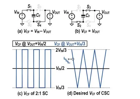
Figs.1(a) and 1(b) show the operation of the charging and discharging phases of the 2 : 1 SC converter.Following Ref.[1], we use ideal voltage sources as input voltageVINand output voltageVOUTin the analysis.The DC value of theCFisVIN/2 when the output voltageVOUT=VIN/2.Fig.1(c) shows the conceptualVCFwaveform, and theCFcharge sharing loss(PCS) is small due to the negligibleVCFripple.However, when we use the 2 : 1 SC converter for aVOUT=VIN/3 operation, thePCSbecomes significant, since theVCFswings fromVIN/3 and 2VIN/3.This makes the conventional SC looks "discontinuous".

Fig.1.(Color online) (a) Charging and (b) discharging phases of a 2 : 1 SC converter, (c) VCF waveforms of 2 : 1 SC converter when VOUT = VIN/2 and VIN/3, and (d) desired VCF waveform of a CSC.
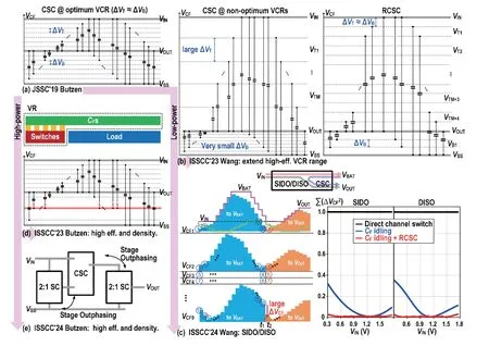
To extend the VCR range with high efficiency, reducing the rising and falling slopes of theVCFis desirable, as shown in Fig.1(d).It can be achieved by splitting the largeVCFswing intoKequal steps, and the resultantPCSshould be reduced byKtimes[11].Based on this idea, work from Ref.[4] made use of multi-phase SC operation (using multipleCFs), generating internal voltage rails forVCFsplitting.As shown in Fig.2(a), taking the step-down conversion as an example, eachCFconnects either its top plate or bottom plate to a DC voltage (VIN,VOUT, orVSS), and the other plate to different internal rails.

Fig.2.(Color online) Recent advancements in CSC DC-DC converters.
(b) Extending high-efficiency VCR range
The CSC’sPCSis determined by theVCFstep size (ΔVCF),i.e.ΔVTfor the step size of the top plate and ΔVBfor that of the bottom plate.Increasing the number of the CSC phases(number ofCFs and switches) reduces the step sizes and thus results in higher efficiency.Unfortunately, this greatly complicates the design, such as 64CFs and 36 × 64 switches in Ref.[4].Hence, under a given design complexity constraint and predefined numbers ofVTandVBsteps (MandN, respectively), the VCR with ΔVT= ΔVBshould have the optimum efficiency.Nevertheless, if the VCR deviates from this value, such as in the example shown in Fig.2(b), the very small ΔVBcontributes little to furtherPCSreduction, while the large ΔVTsignificantly increasesPCS.
Work from Ref.[7] addresses this issue by using reconfigurable-VCFCSC (RCSC).It adapted the value ofMandNto the VCR, with the same design complexity (the sameM+Nvalue), as shown in Fig.2(b).This should further extend the high-efficiency VCR range of CSC.With an overall 19.8-nFCFs,it achieves a maximum 39.7-mW output power.
(c) CSC SIDO/DISO
As shown in Fig.2(c), it is desirable to achieve SIDO and DISO CSC in energy harvesting systems.Work from Ref.[8] proposed a time-multiplexing control (TMC), instead of the ordered-power distributive control (OPDC), to "decouple" the input and output power.
Another issue of SIDO/DISO CSC is the largePCSduring the channel switching.Take nine-CFSIDO CSC as an example.Fig.2(c) shows the transient waveforms of theCFs, where theVCF,nshould have 2 ×TCLKdelay fromVCF,n-1, whereTCLKis the clock period.During switching channel fromVBATtoVOUT(fromt1tot2), it is possible to manipulate the phase of someVCFs for small ΔVCFs, but there still exists some large ΔVCFs,such asVCF9.This degrades the efficiency, meanwhile, the instantaneous large charge-sharing current may damage the switches.
Work from Ref.[8] addressed this by idling certainCFs when supplying the lower output.Then, it incorporated the RCSC scheme to further minimize the ΔVCFs within a wide VCR range.Fig.2(c) shows the calculatedPCS(represented by Σ(VCF)2) normalized to that of the direct channel switching.As seen, theCFidling + RCSC achieves the lowestPCSwithin a wide range.
(d) High power density and efficiency
Work from Ref.[9] used a 4-nm process and high-density on-chip MIM capacitors to implement the CSC as integrated voltage regulator (IVR), for multi-core graphics processing unit (CPU) applications.It also investigated ganging multiple IVR cores to the same load domain.The extremely high maximum current density is 26 A/mm2.
As shown in Fig.2(d), with the loading circuits occupying a large silicon area, it is straightforward to overhang theCFs (consuming top metals) above the loading circuits for a maximumCFvalue (and thus power density).Yet, this inevitably results in long overhang power delivering networks (PDNs), and hence large parasitic resistances and degraded efficiency.
Ref.[9] proposed a phase-merging-turbo (PMT) technique to reduce the resistances, as shown in Fig.2(d).It merged a certain number of internal rails, parallelizing the resistances, and hence improving the heavy-load efficiency.However, the reduced number of internal rails jeopardizes the light-load efficiency.
Work from Ref.[10] investigated the CSC IVR in the scenario of higherVINs for a reduced input current and possibly better system efficiency.It used a 2 : 1 conventional SC to half the input voltage of the CSC, and cascaded another 2 : 1 conventional SC for the targeted low output voltage.This somewhat resembles the design philosophy of recent hybrid DC-DC converters[12-16], where the SC is used to reduce the voltage stress of the switches, and lower the swing of the inductor switching node.After that, outphasing is used between the SC and CSC stages, fulfilling multipleVCFsteps with a reduced number ofCFs.
(e) Future CSC research hot spots
The CSC converter should be able to replace the inductive converter in many applications.However, although without using a bulky inductor, the CSC greatly increases the design complexity, and thus is unfriendly to the layout/PCB design.Implementing so many off-chipCFs is almost impossible.This may be the reason why most works from academia focused on low-power applications.A few works from industry, with high-density on-chip capacitors, achieved high power level.Yet, such capacitors are unavailable in most fabrication processes.Therefore, reducing the complexity of CSC is essential.
Furthermore, the capacitors can give a much larger instantaneous charging current than inductors can do.Consequently, the CSC converter has the potential to fulfill a fast transient response.
Acknowledgment
This work is supported by the Macao Science and Technology Development Fund (FDCT) under Grant 0041/2022/A1,and by the Research Committee of University of Macau under Grant MYRG2022-00004-IME.
 Journal of Semiconductors2024年4期
- Journal of Semiconductors的其它文章
- Electronic origin of structural degradation in Li-rich transition metal oxides: The case of Li2MnO3 and Li2RuO3
- Countermeasure against blinding attack for single-photon detectors in quantum key distribution
- Hybrid bonding of GaAs and Si wafers at low temperature by Ar plasma activation
- Improvement of Ga2O3 vertical Schottky barrier diode by constructing NiO/Ga2O3 heterojunction
- High-speed performance self-powered short wave ultraviolet radiation detectors based on κ(ε)-Ga2O3
- Effect of annealing on the electrical performance of N-polarity GaN Schottky barrier diodes
