Hybrid bonding of GaAs and Si wafers at low temperature by Ar plasma activation
Rui Huang, Zhiyong Wang, Kai Wu, Hao Xu, Qing Wang, and Yecai Guo
1School of Electronic and Information Engineering, Wuxi University, Wuxi 214105, China
2Institute of Advanced Technology on Semiconductor Optics & Electronics, Institute of Laser Engineering, Beijing University of Technology,Beijing 100124, China
Abstract: High-quality bonding of 4-inch GaAs and Si is achieved using plasma-activated bonding technology.The influence of Ar plasma activation on surface morphology is discussed.When the annealing temperature is 300 ℃, the bonding strength reaches a maximum of 6.2 MPa.In addition, a thermal stress model for GaAs/Si wafers is established based on finite element analysis to obtain the distribution of equivalent stress and deformation variables at different temperatures.The shape variation of the wafer is directly proportional to the annealing temperature.At an annealing temperature of 400 ℃, the maximum protrusion of 4 inches GaAs/Si wafers is 3.6 mm.The interface of GaAs/Si wafers is observed to be dense and defect-free using a transmission electron microscope.The characterization of interface elements by X-ray energy dispersion spectroscopy indicates that the elements at the interface undergo mutual diffusion, which is beneficial for improving the bonding strength of the interface.There is an amorphous transition layer with a thickness of about 5 nm at the bonding interface.The preparation of Si-based GaAs heterojunctions can enrich the types of materials required for the development of integrated circuits, improve the performance of materials and devices, and promote the development of microelectronics technology.
Key words: plasma-activated bonding; bonding strength; thermal stress model; mutual diffusion
1.Introduction
Silicon (Si), as the first-generation semiconductor material, directly promotes the development of integrated circuits.Currently, it is still widely used in industries such as electronic information and solar photovoltaic, becoming the cornerstone of materials that promote the innovation and rapid development of microelectronics technology[1-3].However,due to Si being an indirect bandgap semiconductor material,its application field is limited[4].With the continuous reduction of chip feature size, the development of electronic devices has encountered bottlenecks.The traditional Moore’s law has been replaced by the transcendent Moore’s law[5].Devices and modules based on other materials such as compound semiconductors, wide bandgap semiconductors, piezoelectric thin films, and ferroelectric thin film materials are becoming an indispensable part of the information age[6-9].Gallium arsenide (GaAs), as the second-generation semiconductor material, has the advantages of high photoelectric conversion efficiency, high electron mobility (5-6 times that of Si),and high frequency[10].It has been widely used in fields such as semiconductor lasers, microwave devices, high electron mobility transistors (HEMTs), and space solar cells[11-14].However, traditional electronic devices based on GaAs bulk material have problems such as high cost, easy substrate current leakage, and high source/junction capacitation, which affect the performance of GaAs devices.If GaAs materials are integrated onto Si substrates to prepare Si-based GaAs heterojunction, it will overcome the shortcomings of GaAs materials themselves, greatly improve material and device performance, and thus promote the further development of microelectronics technology.
To achieve heterogeneous integration of GaAs materials on Si substrates, the first thing to consider is the mismatch of lattice constants and thermal expansion coefficients between materials.The traditional metal-organic chemical vapor deposition (MOCVD) method is used to epitaxial GaAs thin films on Si substrates, which inevitably introduces high-density reverse domains, threading dislocations, and thermal cracks in the GaAs layer[15].Therefore, it is necessary to find a method to achieve strong bonding between GaAs and Si at low temperatures.Domestic and foreign researchers have conducted extensive and in-depth research in this area.Ohnoet al.[16]prepared GaAs/Si heterojunctions by activating GaAs and Si surfaces with Ar atoms beams.The bonding mechanism of GaAs/Si at room temperature was studied by combining transmission electron microscopy (TEM) and secondary ion mass spectrometry (SIMS) techniques.Yamajoet al.[17]used surface-activated bonding to prepare GaAs/Si heterojunction and found that when the GaAs/Si heterojunction was annealed at 400 ℃, the amorphous transition layer disappeared.However, in the above research results, the bonding rate and bonding strength of GaAs/Si heterojunctions still need to be further improved.
Ar plasma is mainly used to activate GaAs and Si surfaces.The surface morphology and hydrophilicity of GaAs and Si before and after activation are analyzed.Based on finite element analysis, a GaAs/Si thermal stress model is established to simulate the distribution of interfacial thermal stress and shape variables of wafers at different temperatures.The bonding quality of the interface is determined through tensile strength measurement and TEM.The maximum bonding strength of GaAs/Si heterojunction is 6.2 MPa.The electrical characteristic of GaAs/Si heterojunctions at different annealing temperatures is measured.
2.Experimental methods
A 4-inch GaAs (100) wafer with a thickness of 600μm is used in this study.The n-type doping concentration is 2 ×1019cm-3, produced by Freiberger GmbH in Germany.A Si wafer with a thickness of 500μm is also 4-inch with (100) crystal orientation.P-type doping concentration is 1 × 1019cm-3.Before activation, GaAs and Si wafers are placed in alcohol and acetone solutions for ultrasonic cleaning.In order to remove the natural oxide layer present on the wafer surface,GaAs and Si wafers are cleaned in RCA (NH4OH∶H2O2∶H2O = 1∶1∶5) solution and 1% concentration of hydrofluoric acid (HF) solution, respectively.After cleaning, a nitrogen gun is used to blow the surfaces of the wafers.Then the two wafers are separately placed in the inductively coupled plasma (ICP) chamber in Fig.1(a).The air pressure inside the chamber is reduced to 1 × 10⁻⁵Pa.In the chamber, Ar plasma starts to irradiate the surfaces of GaAs and Si wafers,respectively.The irradiation energy of Ar plasma is 2 keV, and the output beam is 1 × 1015cm-2.After activation, the two wafers are bonded together in an atmospheric environment,as shown in Fig.1(b).The applied bonding force is 10 kN and the bonding time is 24 h.After bonding, the bonding rate of GaAs/Si bonding pairs is measured by using an infrared transmission imager.Then, the GaAs/Si wafer pair is cut into bonded square pieces with a size of 10 × 10 mm2.The bonded square pieces are annealed at different temperatures (100, 200, 300, and 400 ℃).Fig.1(c) shows the temperature rise curve at an annealing temperature of 300 ℃, with a slope of 1 ℃/min.
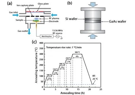
Fig.1.(Color online) (a) Schematic diagram of the plasma-activated wafer; (b) GaAs and Si wafer bonding; (c) time-dependent curve of annealing temperature at an annealing temperature of 300 ℃.
After annealing, the bonding strength of GaAs/Si bonded square pieces is measured at different annealing temperatures using a tensile tester.The bonded square pieces are fixed on the metal fixture with epoxy resin adhesive.The metal fixture is slowly stretched to measure the bonding strength of the square pieces.The roughness and contact angle of the wafer surface before and after activation are measured using an atomic force microscope (AFM) and a hydrophilic angle tester, respectively.A focused ion beam(FIB) is used to thin GaAs/Si samples to meet the observation requirements of TEM.TheI-Vcharacteristic curve of GaAs/Si bonding chips is measured using a metal probe platform.
3.Results and discussion
3.1.Characterization of surface roughness and hydrophilicity
Surface roughness and hydrophilicity have a crucial impact on bonding quality[18].There is a direct correlation between surface roughness and structural damage at the interface.Surface hydrophilicity is used to measure the density of surface hydrophilic groups.The smoother and flatter the surface of the wafer to be bonded, and the higher the density of hydrophilic groups (-OH) on the surface, the more favorable the improvement of bonding quality.The surface roughness and hydrophilicity angle of GaAs and Si wafers before and after activation are measured using AFM and hydrophilicity angle analyzer, as shown in Fig.2.From Figs.2(a) and 2(b), it can be seen that the surface roughness (Ra) of Si before activation is 0.197 nm, and the surface contact angle is 80.5°.After Ar plasma irradiation, the surface roughness becomes 0.235 nm and the surface contact angle decreases to 4.5°.Similarly, from Figs.2(c) and 2(d), it can be seen that the surface roughness of GaAs before activation is 0.210 nm, and the surface contact angle is 78.6°.After Ar plasma irradiation, the surface roughness becomes 0.325 nm and the surface contact angle decreases to 2.5°.Although the Ar plasma irradiation can increase the surface roughness of the wafer to some extent, the smoothness and flatness of the wafer surface still meet the requirements of bonding.In addition, the Ar plasma irradiation can generate more dangling bonds on the wafer surface, which cannot exist stably in their natural state.They need to combine with surrounding hydroxyl groups (-OH) to form a stable structure, ultimately enhancing the hydrophilicity of the wafer surface.Therefore, by comparing the changes of -OH groups on the surfaces of GaAs and Si before and after Ar plasma activation, it can be indirectly determined whether more dangling bonds have been generated.From Figs.2(e) and 2(f), it can be seen that the intensity of oxide peaks on the wafer surface has been enhanced after activation, indicating an increase in the number of -OH groups attached to the surface.This result can indirectly indicate that more dangling bonds are formed after Ar plasma irradiation.
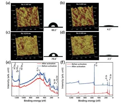
Fig.2.(Color online) (a) Before surface activation of Si wafer; (b) after surface activation of Si wafer; (c) before surface activation of GaAs wafer; (d)after surface activation of GaAs wafer; (e) XPS survey on GaAs surface before and after Ar plasma-activation; (f) XPS survey on Si surface before and after Ar plasma-activation.
3.2.Bonding strength and bonding rate
Fig.3 shows the physical image and infrared transmission imaging schematic of a 4-inch GaAs/Si bonding pair.From Fig.3(b), it can be seen that most areas of the GaAs/Si wafer have been bonded together, and there are no contaminated particles or voids in the middle.However, a small number of unbonded areas exist at the edges of the GaAs/Si wafer.The bonded wafer is fixed with paraffin on the base of the cutting machine, and a diamond cutting knife is used to cut the 4-inch GaAs/Si bonding wafer, as shown in Fig.3(c).From Fig.3(c), it can be seen that a portion of the 4-inch GaAs/Si bonding wafer has been cut into 10 × 10 mm2bonded square pieces.From the above cutting process, it can be seen that the pre-bonding strength of GaAs/Si can withstand the influence of shear stress applied by mechanical cutting.After the wafer is cut, the bonded square pieces are placed in annealing furnaces for annealing processes at different temperatures (100, 200, 300, and 400 ℃).The annealing temperature of 300 ℃ is taken as an example.The temperature variation curve of the annealing furnace with time is shown in Fig.1(c).Annealing can further enhance the bonding strength of GaAs/Si heterojunctions.After annealing, the bonding strength of bonded square pieces is measured at different annealing temperatures using a tensile strength measuring instrument.Due to the small size and thin thickness of the sample, it is difficult to clamp it on the stretching equipment.Therefore, epoxy resin adhesive is applied to the upper and lower surfaces of the bonding pair and bonded to the stretching rod.The tensile equipment used in the experiment is the Instron 5569 electronic universal material testing machine produced by Instron company in the US.The stretching rate of the equipment is controlled at 1 mm/min.The bonding strength of GaAs/Si bonding pairs is measured under different conditions.Fig.3(d) shows the bonding strength of GaAs/Si bonded square pieces measured at different annealing temperatures.From the graph, it can be seen that during the heating process from room temperature to 300 ℃, the bonding strength of GaAs/Si gradually increases,reaching a maximum value of 6.2 MPa at 300 ℃.When the annealing temperature is further increased to 400 ℃, the thermal stress at the bonding interface further increases, leading to a decrease in GaAs/Si bonding strength.Therefore, the optimal annealing temperature for GaAs/Si heterojunctions can be determined to be 300 ℃.

Fig.3.(a) Physical image of GaAs/Si bonded wafers; (b) infrared transmission imaging of GaAs/Si bonded wafers; (c) schematic diagram of a GaAs/Si bonding pair cut into 10 × 10 mm2 bonded square pieces; (d) relationship diagram of GaAs/Si bonding strength at different annealing temperatures.
3.3.Characterization of GaAs/Si bonding interface morphology
After the bonding strength of GaAs/Si square pieces is measured at different temperatures, TEM is used to image the GaAs/Si bonding interface.Before imaging, it is necessary to conduct an overall evaluation of the interface morphology.Scanning electron microscopy (SEM) is utilized to observe the overall interface morphology, as shown in Fig.4(a).From the figure, it can be seen that the GaAs/Si square pieces have a relatively dense bonding.The cross-section of Si wafers is relatively flat and smooth, while the crosssection of GaAs wafers is relatively rough.GaAs materials are brittle and have lower hardness than Si.Therefore, before preparing samples for GaAs/Si square plates, it is necessary to perform ion beam polishing on their cross-section to ensure that the roughness on the cross-section meets the requirements.After polishing, the GaAs/Si sample is placed in the FIB chamber.Before sample preparation, metal platinum (Pt)as a protective layer is sprayed at the position to be prepared, as shown in Fig.4(b).After spraying, FIB is used to extract the sample at the position to be prepared.Then, the extracted sample is fixed on a metal copper mesh, as shown in Fig.4(c).After fixation, the GaAs/Si bonding interface is thinned layer by layer until it meets the requirements for TEM observation.
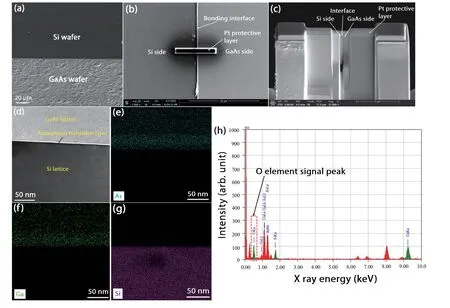
Fig.4.(Color online) (a) SEM image of GaAs/Si bonding interface; (b) the GaAs/Si bonding interface is coated with a protective Pt layer; (c)GaAs/Si sample is thinned; (d) schematic diagram of GaAs/Si bonding interface; (e) the distribution of As element at the bonding interface; (f) the distribution of Ga element at the bonding interface; (g) the distribution of Si element at the bonding interface; (h) elemental composition of amorphous transition layer of GaAs/Si wafers.
After the preparation of GaAs/Si samples, they are placed under TEM for observation.From Fig.4(d), it can be seen that there is an amorphous transition layer with a thickness of about 5 nm at the interface.There is a transition layer between GaAs and Si lattices.The regular arrangement of GaAs and Si lattices is displayed on both sides of the transition layer.The atoms of bonding interface are in close contact, and no cracks or voids are observed.We conduct energy dispersive scanning analysis on the element distribution at the interface, characterizing the distribution of As, Ga, and Si elements.From Figs.4(e)-4(g), it can be seen that the three elements undergo mutual diffusion at the interface.The mutual diffusion between atoms is beneficial for enhancing the bonding strength of GaAs/Si heterojunctions.In order to further determine the elemental composition of the amorphous transition layer, we select a point in the amorphous layer for X-ray energy dispersion spectrum analysis and obtained the results shown in Fig.4(h).From the figure, it can be determined that the intermediate amorphous transition layer is mainly composed of four elements: As, Ga, O,and Si.Although we have used RCA and HF solutions to remove the original oxide layers on the GaAs and Si surfaces before the experiment, the wafer surfaces are inevitably oxidized during the experimental process.The inclusion of oxides in the amorphous layer affects the electrical properties of the interface, limiting the transport of charge carriers.
3.4.Analysis of GaAs/Si bonding interface characteristics
In order to analyze the mechanical properties of the GaAs/Si bonding interface, we have established a GaAs/Si wafer model based on finite element analysis, as shown in Fig.5.During the simulation process, the thickness, Young's modulus, coefficient of thermal expansion (CTE), and Poisson's ratio of GaAs are set to 600μm, 8.526 × 10¹⁰Pa,6.4 × 10-6K-1and 0.31 respectively.The thickness, Young's modulus, CTE, and Poisson's ratio of Si are set to 500μm,1.66 × 1011Pa, 2.6 × 10⁻⁶K-1and 0.29 respectively.The position relationship between GaAs and Si is set to bonding.We simulate they-direction displacement cloud,z-direction displacement cloud, interface equivalent stress, and wafer shape variables generated by the bonding structure when the model is annealed from 100, 200, 300, and 400 ℃ to room temperature (25 ℃).As the temperature changes, the wafer bonding interface will generate shear stress and normal stress parallel to the interface, as well as peel stress perpendicular to the interface[19].As shown in Fig.5(a), there is a significant positive displacement at the edge position.GaAs and Si wafers are more prone to slip and generate dislocations.At this point, the shear stress and peel stress at the bonding interface have a stable stress distribution in the middle region of the chip, but the equivalent stress increases sharply in the edge region, as shown in Fig.5(c).In addition, due to the effect of bending moment, the central region of the GaAs/Si wafer structure protrudes upwards, forming the structure shown in Fig.5(b).The variation curve of GaAs/Si wafer protrusion under different annealing temperatures based on finite element analysis simulation is obtained, as shown in Fig.5(d).Because the GaAs wafer is on top and the Si wafer is on bottom, and the CTE of GaAs is greater than that of Si, when the same annealing temperature is raised, the thermal expansion deformation of GaAs is greater than that of Si.Due to the bonding state between GaAs and Si, they cannot be separated, resulting in a convex shape as shown in Fig.5(d).The four curves in Fig.5(d) show the distribution of crystal circular variables at 100, 200, 300, and 400 ℃, respectively.In theory, the convex deformation of GaAs/Si wafers is directly proportional to the annealing temperature.At an annealing temperature of 400 ℃, the maximum protrusion is 3.6 mm.
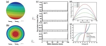
Fig.5.(Color online) (a) Y-direction displacement cloud map; (b) z-direction displacement cloud map; (c) the distribution curve of equivalent stress and wafer diameter; (d) distribution curve of wafer variables and diameter; (e) analysis of electrical characteristics of GaAs/Si bonding interface at different annealing temperatures.
In addition to analyzing the thermal stress on the GaAs/Si bonding interface, we have also evaluated the electrical properties of the GaAs/Si heterojunction interface at annealing temperature and obtained theI-Vcharacteristic curves as shown in Fig.5(e).The doping concentration of ntype GaAs crystal is 2 × 1019cm-3, and the doping concentration of p-type Si crystal is 1 × 1019cm-3.P-type and n-type metal electrodes are deposited on the surface of GaAs/Si heterojunctions prepared under different conditions.Then, the electrical characteristic curves of GaAs/Si heterojunctions are obtained at annealing temperatures of 200 , 300 , and 400 ℃.From the figure, it can be seen that as the annealing temperature increases, the current density of GaAs/Si bonded chips is higher at the same voltage.This indicates that an increase in annealing temperature can, to some extent, repair lattice defects at the bonding interface, thereby improving the transport capacity of interface carriers.However, an increase in annealing temperature also increases the thermal stress at the interface, reducing the bonding strength of GaAs/Si.
3.5.GaAs/Si bonding mechanism
Plasma-activated bonding requires wafers to have high flatness, parallelism, and smoothness.At the same time, it is also necessary to ensure that the surface is clean and free from particles, organic matter, and metal pollution.Therefore,it is crucial to clean the wafer before processing.The surface exhibits strong hydrophobicity before the activation of GaAs and Si wafers.When Ar plasma is used to irradiate the surface of the wafer, the surface exhibits strong hydrophilicity.Ion beam activation can make the surface of the wafer rough to some extent, but it also generates more dangling bonds on the surface.Dangling bonds cannot exist stably under natural conditions and require the adsorption of alcohol hydroxyl groups (-OH) from the surrounding environment to reach a stable state.When two wafers are activated and bonded together at room temperature, it is called pre-bonding.Prebonding is mainly caused by the capillary force, electrostatic force, van der Waals force, and hydrogen bonding between two wafers, which bonds the wafers together.At this time,the bonding strength is relatively weak.Therefore, it is necessary to perform an annealing process on it.The increase in temperature can promote the diffusion of interfacial water molecules to both sides, while accelerating the transition of silanol groups to siloxane bonds, resulting in the following reactions[20]:
High-temperature treatment can convert weak bonds at the interface into covalent bonds, resulting in sufficiently high interfacial energy.In addition, the introduction of the O element at the interface can increase the interface volume, fill the nano-gaps between the interfaces, and thus close the interface.The increase in temperature will also lead to the reaction between GaAs and Si on both sides of the interface and H2O molecules, generating corresponding oxides and H2.Furthermore, it absorbs additional H2O molecules, increases the thickness of the oxide layer, and leads to the formation of an amorphous transition layer.
4.Conclusion
High-quality wafer bonding of 4-inch GaAs/Si is achieved through Ar plasma-activated bonding.As the annealing temperature increases, the bonding strength of GaAs/Si gradually increases.When the annealing temperature is 300 ℃, the GaAs/Si bonding strength reaches a maximum value of 6.2 MPa.As the annealing temperature further increases, the bonding strength begins to decrease.Therefore, the optimal annealing temperature for GaAs/Si heterojunctions is 300 ℃.A GaAs/Si wafer bonding model is also established based on finite element analysis to simulate the distribution of interface equivalent stress and crystal circular variables at different annealing temperatures.The shear stress and peel stress at the bonding interface have a stable stress distribution in the middle region of the chip, but the equivalent stress increases sharply in the edge region.At an annealing temperature of 400 ℃, the maximum protrusion of GaAs/Si wafers is 3.6 mm.The electrical properties of the GaAs/Si heterojunction interface at different annealing temperatures are obtained, and the conductivity of the interface is directly proportional to the annealing temperature.This indicates that the annealing process can to some extent repair interface lattice defects and enhance interface carrier transport capacity.This study has achieved the bonding of Si and GaAs using the plasma-activated bonding method.By optimizing the activation and annealing processes, the optimal bonding effect of Si-based GaAs is achieved.The research results provide alternative technological reserves for promoting the development of integrated circuits.
Acknowledgments
This work was financially supported by the National Nature Science Foundation of China (Grant No.61673222),the Natural Science Foundation of the Jiangsu Higher Education Institutions of China (Grant No.23KJB430036), and Wuxi University Research Start-up Fund for Introduced Talents(Grant No.2022r036).
 Journal of Semiconductors2024年4期
- Journal of Semiconductors的其它文章
- Electronic origin of structural degradation in Li-rich transition metal oxides: The case of Li2MnO3 and Li2RuO3
- Countermeasure against blinding attack for single-photon detectors in quantum key distribution
- Improvement of Ga2O3 vertical Schottky barrier diode by constructing NiO/Ga2O3 heterojunction
- High-speed performance self-powered short wave ultraviolet radiation detectors based on κ(ε)-Ga2O3
- Effect of annealing on the electrical performance of N-polarity GaN Schottky barrier diodes
- On the relationship between imprint and reliability in Hf0.5Zr0.5O2 based ferroelectric random access memory
