High-speed performance self-powered short wave ultraviolet radiation detectors based on κ(ε)-Ga2O3
Aleksei Almaev, Alexander Tsymbalov, Bogdan Kushnarev, Vladimir Nikolaev, Alexei Pechnikov,Mikhail Scheglov, Andrei Chikiryaka, and Petr Korusenko
1Research and Development Center for Advanced Technologies in Microelectronics, National Research Tomsk State University, Tomsk 634050,Russia
2Fokon LLC, Kaluga 248035, Russia
3Department of Semiconductor Electronics and Physics of Semiconductors, National University of Science and Technology MISIS, Moscow 119049, Russia
4Perfect Crystals LLC, Saint Petersburg 194223, Russia
5Department of Solid-State Electronics, Saint Petersburg State University, Saint Petersburg 199034, Russia
6Department of Physics, Omsk State Technical University, Omsk 644050, Russia
Abstract: High-speed solar-blind short wavelength ultraviolet radiation detectors based on κ(ε)-Ga2O3 layers with Pt contacts were demonstrated and their properties were studied in detail.The κ(ε)-Ga2O3 layers were deposited by the halide vapor phase epitaxy on patterned GaN templates with sapphire substrates.The spectral dependencies of the photoelectric properties of structures were analyzed in the wavelength interval 200—370 nm.The maximum photo to dark current ratio, responsivity, detectivity and external quantum efficiency of structures were determined as: 180.86 arb.un., 3.57 A/W, 1.78 × 10¹² Hz0.5·cm·W-1 and 2193.6%, respectively, at a wavelength of 200 nm and an applied voltage of 1 V.The enhancement of the photoresponse was caused by the decrease in the Schottky barrier at the Pt/κ(ε)-Ga2O3 interface under ultraviolet exposure.The detectors demonstrated could functionalize in self-powered mode due to built-in electric field at the Pt/κ(ε)-Ga2O3 interface.The responsivity and external quantum efficiency of the structures at a wavelength of 254 nm and zero applied voltage were 0.9 mA/W and 0.46%, respectively.The rise and decay times in self-powered mode did not exceed 100 ms.
Key words: κ(ε)-gallium oxide; solar-blind shortwave ultraviolet radiation detectors; self-powered operation mode
1.Introduction
Solar-blind ultraviolet detectors (SBUVDs) are of large research and technological interest due to their potential in a pallet of applications such as flame sensors, space communications, control systems, ozone holes localization, navigation,etc.[1].Gallium oxide (Ga2O3) is a very promising semiconductor for the development of SBUVDs due to its ultra-wide band gap energy value ofEg= 4.4—5.5 eV, and excellent stability in harsh environments especially under radiation[1-7].Ga2O3has several polymorphs.The thermodynamically stable one is the monoclinicβ-Ga2O3polymorph, which has been the most studied within the last decade[8].Several polymorphs of Ga2O3have been identified such as:α,δ,γandκ(ε)[3,9-11].
The metastableκ(ε)-Ga2O3polymorph hasEg= 4.4—4.9 eV and the thermal stability up to 700 ℃, that make possible to compete with theβ-Ga2O3polymorph in certain applications[12,13].The prospects ofκ(ε)-Ga2O3for the development of Schottky barrier and p-n heterojunction diodes[14-16], a high electron mobility transistors[17-20], a gas sensors[21,22], a X-ray detectors[23]and SBUVDs[24-34]were demonstrated already.Moreover, theκ(ε)-Ga2O3crystal belongs to the hexagonal syngony and therefore, it has a good crystallographic matching with sapphire and Ⅲ-nitride crystals, which is of interest for the development of novel optoelectronic devices like e.g., matrix photodetectors[35].These devices require a high uniformity of the active layer of the heterostructure[34,36,37].Theκ(ε)-Ga2O3can satisfy this requirement due to its low concentrations of defects at the interface and high crystalline symmetry compared with the low-symmetry monoclinicβ-Ga2O3[4].
Halide vapor phase epitaxy (HVPE) is a well-established inorganic chemical vapour deposition method for heteroepitaxial growth of GaN, which recently has been employed to grow different Ga2O3polymorphs of high quality, e.g., the metastableα-Ga2O3andκ(ε)-Ga2O3polymorphs[20,38,39-43].The metal-semiconductor-metal (MSM) structures based on HVPE depositedα-Ga2O3demonstrated high response to shortwave ultraviolet radiation[44-46].HVPE allows to deposit high quality metastableα-Ga2O3andκ(ε)-Ga2O3polymorphs layers with thicknesses in the wide interval.This method is characterized by a high deposition rate combined with uniform ntype doping[38].Nevertheless, of the advantages discussed above, the photoelectric properties of HVPE depositedκ(ε)-Ga2O3are practically unexplored.That is why, the goal of our research is to gain insight into the photoelectric properties of MSM-structures based on the HVPE depositedκ(ε)-Ga2O3layers.
The innovative nature of our work is the research and development of self-powered SBUVDs based on HVPE-κ(ε)-Ga2O3layers with the highest operation rate among same devices based onκ(ε)-Ga2O3.Such devices have a number of advantages: not required external power; high-speed performance; stability of characteristics[5].In addition, the operating spectral range of the detectors demonstrated lays at a wavelength shorter than 280 nm, and the devices do not require utilization of optical filters.
2.Materials and methods
Theκ(ε)-Ga2O3layer deposition was multi-staged.At the first step, a semi-insulating (SI) GaN layer was deposited by the industry-relevant metal organic chemical vapor phase deposition, providing deposition of semiconductors of high quality and homogeneity on large areas[47-49], on the c-plane patterned sapphire substrates (PSS).The SI-GaN was a template for theκ(ε)-Ga2O3layer.At the second step, aκ(ε)-Ga2O3layer was deposited on the SI-GaN by the HVPE, employing a hot-wall home-made reactor providing high thickness and properties homogeneity on large areas[11,20,22].Vapor phase GaCl and O2were utilized as precursors for elemental Ga and oxygen.GaCl vapors was produced by the reaction of metallic Ga and gaseous HCl.The molar flow ratio of the Ⅴ/Ⅲ components was 4.2.Argon was used as the carrier gas.The total flow of Ar was kept at 10 slm.The optimal HVPE deposition temperature for formation of theκ(ε)-Ga2O3polymorph was determined as 630 ℃.The deposition rate during HVPE was~1.56μm/h.Intentional doping of theκ(ε)-Ga2O3films during the HVPE growth process was not performed.
Pt interdigital contacts were formed on theκ(ε)-Ga2O3layers by means of magnetron sputtering with following photolithography.The interelectrode distance was 300μm.The device wafer prepared was divided into chips with 5 mm ×5 mm in size (Fig.1).The effective areaSof the samples surface exposed to irradiation was 7.6 mm2.
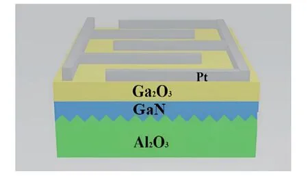
Fig.1.(Color online) A schematic view of SBUVD-based on the HVPE deposited κ(ε)-Ga2O3 layer.
The phase composition and degree of crystallinity of the samples were examined by X-ray diffraction (XRD) by means of a DRON 6 diffractometer (Bourevestnik, JSC) with CuKαradiation at wavelengthλ= 1.5406 Å.The cross-sectional images of the samples were studied by a scanning electron microscope (SEM) (Phenom ProX, The Netherlands) at accelerating voltage of 10 kV.The transmission spectra of theκ(ε)-Ga2O3layers were calculated from the reflection spectra initially measured by means of a ultraviolet-visible (UV-VIS) spectrophotometer (Analytik Jena, Germany) in the interval ofλ=230—360 nm.
The spectral dependencies of the photoelectric properties were measured by means of the spectrometric system based on a MonoScan 2000 monochromator (Ocean Optics)and a DH-2000 Micropack lamp, described in detail in Ref.[46].A krypton-fluorine lamp VL-6.C was used as the source of irradiation atλ= 254 nm and the light power densityP= 620μW/cm2.The photoelectric and electrical properties of the samples were measured by means of Keithley 2636 A.
3.Results and discussion
3.1.Structural properties of the HVPE deposited κ(ε)-Ga2O3
A typical XRD spectrum of the structure is illustrated in Fig.2(a).The XRD peaks at 2θ= 18.7°, 38.6°, 59.5°, 83.1°, and 112.1° correspond to (002), (004), (006), (008), and (0010)Bragg reflections of theκ(ε)-Ga2O3[50,51], respectively.The other high intensity peaks appearing at 2θ= 41.4°, 90.5° and 34.3°, 72.6° belong to (0006) and (00012) reflections of the Al2O3substrate, (002) and (004) reflections of the GaN layer,respectively.Obviously, we have achieved heteroepitaxial growth of theκ(ε)-polymorph of Ga2O3on GaN buffered sapphire.
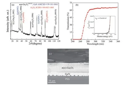
Fig.2.(Color online) (a) A typical XRD spectrum of the HVPE deposited κ(ε)-Ga2O3 layer on GaN/Al2O3.(b) Transmission spectrum of the HVPE deposited κ(ε)-Ga2O3 layer.Dependence of α2 on photons energy is shown in insertion.(c) SEM cross-sectional image of the κ(ε)-Ga2O3 layer on GaN/Al2O3.
TransmittanceTof the samples in the interval ofλ=300—360 nm is measured to be within the interval 63%—66%(depicted in Fig.2(b)).Obviously, the sharp drop ofTwith decrease ofλfrom 285 to 260 nm is caused by the interband photons absorption.There are no impurity tails in theT(λ)dependence.TheEgof the samples is 4.72 ± 0.05 eV and corresponds to the literature data[19,25,28,29,34].In Fig.2(b),αis the absorption coefficient.
According to the SEM study (Fig.2(c)), the thicknesses of theκ(ε)-Ga2O3and GaN layers are ~13.1μm and ~4.5 μm,respectively.A clear boundary contrast is observed at the interfaces ofκ(ε)-Ga2O3/GaN and GaN/PSS.
3.2.Photoelectric properties of HVPE deposited κ(ε)-Ga2O3
The current—voltageI—Vcurves of the samples are approximated by power functionI~Ul(Fig.3), whereUis the applied voltage;lis the power index,l= 3.32 ± 0.03 and 2.54 ± 0.01 in dark condition and under radiation exposure,respectively.TheI—Vcurves are typical for MSM structures with a Schottky barrier at metal/semiconductor interfaces.The dark currentIDrises withUmore significant than the total currentIL.IDincreases from 0 to 43.5μA andILincreases from 55.3 nA to 197μA with increase ofUfrom 0 to 3 V.The noticeable conductivity of the HVPEκ(ε)-Ga2O3layers in dark conditions is due to the presence of intrinsic electrically active defects of donor-type.Such defects in the HVPEκ(ε)-Ga2O3layers were investigated by our group in detail in Ref.[20], however, their nature has not been definitively established yet.

Fig.3.(Color online) I—V curves of the samples in dark conditions and under radiation exposure.
Dependencies of the photo to dark current ratio (PDCR),responsivityR, detectivityD,and external quantum efficiency(EQE) of samples on λ andUwere computed by means of following formulas, consequently:
whereIphis the photocurrent,Iph=IL—ID;his the Planck constant,cis the speed of light in vacuum;qis the electron charge.Eq.(3) allows to estimateDin case of the SBUVD noise related with the noise ofID[2].This formula does not take into account other types of noise that occur during the manifestation of the photoresponse enhancement.However,it is often used to evaluateDin this case[1,2,27,29].
The samples demonstrate weak sensitivity to irradiation atλ≥ 280 nm (Fig.4).A slight increase of the PDCR,R,DandEQE in the interval ofλ= 280—340 nm is due to the presence of GaN template.The sharp increase in PDCR,R,Dand EQE with a drop of λ from 260 to 200 nm is caused by the interband photons absorption in theκ(ε)-Ga2O3.The maximum values of the photoelectric properties are observed atλ=200 nm.The PDCR,R, EQE andDatλ= 200 nm andU= 1 V are determined to have the following values: 180.86 arb.un.,3.57 A/W, 2193.6% and 1.78 × 10¹²Hz0.5·cm·W-1, respectively.
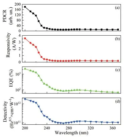
Fig.4.(Color online) Spectral dependencies of the PDCR (a), R (b), EQE(c) and D (d) of the MSM structures at U = 1 V.
Fig.5 shows the dependencies of photoelectric properties of the samples studied onU.These dependencies are determined by theI—Vcurves in dark conditions and under radiation exposure and are approximated by power function with power indexes of —0.96 ± 0.05, 2.36 ± 0.01, 0.58 ± 0.02 for PDCR,Rand EQE,D, respectively.TheR, EQE andDsignificantly increase with an increase inUfrom 0.1 to 3 V.TheR,EQE andDatλ= 254 nm,P= 620μW/cm2andU= 3 V have been determined as: 2.60 A/W, 1272.9% and 1.92 ×10¹¹Hz0.5·cm·W-1, respectively.On the contrary, the PDCR is significantly reduced with an increase inUfrom 0.1 to 3 V(Fig.5(a)) due to rise of the dark current (Fig.3).The PDCR atU= 3 V is 3.54 arb.un.More interesting is the fact that theIphatλ= 254 nm,P= 620μW/cm2andU= 0 was 55.3 nA.Obviously, the samples are applicable for the self-powered operation mode.TheRand EQE in the self-powered operation mode (atU= 0) have 0.9 mA/W and 0.46%, respectively.
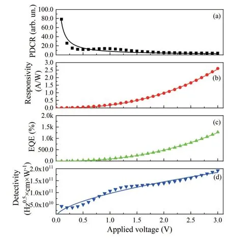
Fig.5.(Color online) Dependencies of the PDCR (a), R (b), EQE (c) and D (d) of the MSM structures on U at λ = 254 nm and P = 620 μW/cm2.
The operation rate of the SBUVDs was studied in the selfpowered operation mode.The riseτrand the decayτdtimes were determined as the time interval between 0.9 and 0.1 levels of the maximumIL(Fig.6).τrandτddo not exceed 100 ms.The self-powered HVPEκ(ε)-Ga2O3SBUVD are characterized by fast photoresponse.It is worth noting that the equipment used to measure the photoelectric properties does not allow to measure theτrandτdat <100 ms with a high accuracy.
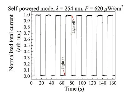
Fig.6.(Color online) Time dependence of the normalized IL at cyclic radiation exposure at λ = 254 nm, P = 620 μW/cm2 and U = 0.
The existence of a built-in electric field at the Pt/κ(ε)-Ga2O3interface gives the capability of the HVPEκ(ε)-Ga2O3-based SBUVDs to functionalize in the self-powered operation mode.The self-powered operation mode of SBUVDs was discussed in detail in Refs.[52-54].The built-in electric field separates the photo-generated free charge carriers that lead to appear an electric current in the circuit.
In Table 1 the photoelectric properties of self-powered SBUVDs based on different Ga2O3polymorphs from literature and our achievements are compared.In Table 1: NWs is the nanowires;a-Ga2O3is the amorphous Ga2O3; HJ is the heterojunction; SBD is the Schottky barrier diode.In comparison with the results of other works the samples studied are characterized by lowτrandτd, relatively high values of theR.

Table 1.Comparison of the photoelectric properties of self-powered SBUVDs based on diverse Ga2O3 polymorphs.
SBUVDs based on the HVPEκ(ε)-Ga2O3layers are characterized by high sensitivity to UV radiation, but their operation rate is still low in comparison with commercial devices.The characteristics of the commercial SBUVDs were summarized in our previous work[46].Matrix SBUVDs are of interest for many practical applications.In addition, the HVPE growth process of theκ(ε)-Ga2O3layers should be further optimized for the development of simultaneously highly sensitive, highspeed performance and cost-effective SBUVDs.Thus the future research and developments are directed to improve the operation rate of the SBUVDs, to develop matrix detectors based on HVPEκ(ε)-Ga2O3layers as well as to optimize the HVPE process in order to produce cost-effective SBUVDs based onκ(ε)-Ga2O3layers.
Notably, the high values of photoelectric properties exhibited in Fig.4 and Fig.5 indicate the manifestation of an enhancement of photoresponse.We had been reporting that self-localization of holes is the main mechanism of an enhancement of the photoresponse for the MSM structure based on the HVPE depositedα-Ga2O3layer with ohmic Ni/Ti contacts[46,65].Therefore, reducing of the potential barrier at metal/semiconductor interfaces is also feasible mechanism of an enhancement of the photoresponse for the MSM structure composed of the HVPE depositedκ(ε)-Ga2O3layer with Pt contacts.The current flowing through the Schottky barrier is described by following expressions[29]:
whereIsis the saturation current;nis the ideality factor;kis the Boltzmann constant;TKis the absolute temperature;Ais the Richardson constant;φbis the Schottky barrier.Theφbvalue can be compute from Eqs.(5) and (6)[66,67]:
The assessments by means of Eqs.(5)—(7) showed that theφbvalues were 1.05 and 0.89 eV in dark conditions and under radiation exposure atλ= 254 nm andP= 620μW/cm2.Theφbvalues in dark conditions correspond to literature data[68].A decrease inφbvalues by 0.16 eV under irradiation occurs due to the accumulation of self-trapped holes near the electrode’s regions[69-71].
4.Conclusion
We have developed and demonstrated the advantages of shortwave ultraviolet radiation detectors based on theκ(ε)-Ga2O3layers with Pt interdigital contacts.13.1μm thickκ(ε)-Ga2O3layers were deposited by the halide vapor phase epitaxy on the patterned sapphire substrates with a GaN template.The spectral dependencies of the photoelectric properties of structures were analyzed in the wavelength interval of 200—370 nm.The detectors based on HVPE depositedκ(ε)-Ga2O3demonstrated a significant response to shortwave ultraviolet radiation with a wavelength no more than 260 nm.The maximum photo to dark current ratio, responsivity, detectivity and external quantum efficiency of structures were 180.86 arb.un., 3.57 A/W, 1.78 × 10¹²Hz0.5·cm·W-1and 2193.6%, respectively, at a wavelength of 200 nm and applied voltage of 1 V.The high values of the photoelectric properties were caused by the manifestation of an enhancement of the photoresponse mainly due to a decrease in the Schottky barrier at the Pt/κ(ε)-Ga2O3interface under ultraviolet radiation exposure.The detectors had sensitivity to shortwave ultraviolet radiation at zero applied voltage and could functionalize in self-powered operation mode due to built-in electric field at the Pt/κ(ε)-Ga2O3interfaces.The responsivity and external quantum efficiency of structures at a wavelength of 254 nm and zero applied voltage were 0.9 mA/W and 0.46%, respectively.The rise and decay times in self-powered operation mode do not exceed 100 ms, i.e., detectors developed are fast responding.
Acknowledgments
Research of the photoelectric properties of theκ(ε)-Ga2O3films was supported by the Russian Science Foundation,grant number 20-79-10043-P.Fabrication of the ultraviolet detectors based on theκ(ε)-Ga2O3layers was supported by the grant under the Decree of the Government of the Russian Federation No.220 of 09 April 2010 (Agreement No.075-15-2022-1132 of 01 July 2022).Research of the structural properties of theκ(ε)-Ga2O3was supported by the St.Petersburg State University, grant number 94034685.
 Journal of Semiconductors2024年4期
- Journal of Semiconductors的其它文章
- Electronic origin of structural degradation in Li-rich transition metal oxides: The case of Li2MnO3 and Li2RuO3
- Countermeasure against blinding attack for single-photon detectors in quantum key distribution
- Hybrid bonding of GaAs and Si wafers at low temperature by Ar plasma activation
- Improvement of Ga2O3 vertical Schottky barrier diode by constructing NiO/Ga2O3 heterojunction
- Effect of annealing on the electrical performance of N-polarity GaN Schottky barrier diodes
- On the relationship between imprint and reliability in Hf0.5Zr0.5O2 based ferroelectric random access memory
