
Ultrafast carrier dynamics in GeSn thin film based on time-resolved terahertz spectroscopy
2024-01-25 07:11:12PanpanHuang黄盼盼YouluZhang张有禄KaiHu胡凯JingboQi齐静波DainanZhang张岱南andLiangCheng程亮
Chinese Physics B 2024年1期
关键词:张岱
Panpan Huang(黄盼盼), Youlu Zhang(张有禄), Kai Hu(胡凯), Jingbo Qi(齐静波),3,†,Dainan Zhang(张岱南),,‡, and Liang Cheng(程亮),3,§
1School of Electronic Science and Engineering,Universityof ElectronicScience and Technology of China,Chengdu 611731,China
2StateKeyLaboratory ofElectronic ThinFilmsand IntegratedDevices,UniversityofElectronicScienceandTechnologyofChina,Chengdu611731,China
3School of Physics,University ofElectronicScienceandTechnologyof China,Chengdu611731,China
Keywords: GeSn thin film,time-resolved THz spectroscopy,ultrafast dynamics,carrier recombination
1.Introduction
Ge1−xSnx(abbreviated as GeSn)materials have attracted increasing attention in the fields of microelectronics and optoelectronics due to their excellent optoelectronic properties and good compatibility with mature Si-based technology.[1,2]When the Sn concentration of GeSn is in the range ofx~0.06–0.1, a transition from an indirect bandgap to a direct bandgap occurs,and this tunable band structure enables GeSn to have multiple applications.[3–5]Furthermore,due to its high carrier mobility, GeSn can be used to fabricate novel electronic devices.[6–9]It also exhibits excellent optoelectronic properties in the infrared range, and can be used as a luminescent material to fabricate infrared light sources.[4,10–14]Moreover, GeSn can be used for infrared detection, and the bandgap width of GeSn can be adjusted by tuning the Sn content,enabling the tuning of the infrared detection range.[15,16]Therefore, optoelectronic devices based on GeSn have enormous potential for application in various fields, such as freespace and fiber-optic communication, optoelectronic detection, monitoring and identification, artificial intelligence, and medical imaging,among others.
At higher doping concentrations, GeSn alloy transforms into a direct bandgap semiconductor,[3,4]and exhibits good performance in the infrared range.In order to apply this material,it is necessary to understand the interaction between infrared photons and the material, especially the carrier relaxation behavior after photoexcitation and the electrical properties of the generated carriers.Therefore, we perform timeresolved terahertz spectroscopy (TRTS)[17–19]to measure the epitaxial grown GeSn thin films.
2.Samples and experimental setup
In our work, the sample is GeSn thin film grown on Si substrate using the molecular beam epitaxy (MBE) method.Before the growth, the chamber base pressure is kept at approximately 4×10⁻⁹Torr.During growth, the temperature of the Ge source is set at 1200°C with a heating rate of 7°C/min, the temperature of the Sn source is set at 1050°C with a heating rate of 5°C/min,and the substrate temperature is set at 150°C with a heating rate of 3°C/min.The growth time is 2 hours, resulting in the film thickness of approximately 120 nm.The Sn concentration in the prepared GeSn film is confirmed by x-ray photoelectron spectroscopy(XPS)as approximately 22.34%, which is heavily doped and makes the GeSn sample as a direct bandgap semiconductor with a bandgap<0.25 eV.[20]Therefore, in the following study, we choose a light source with wavelength of 2500 nm(photon energy~0.5 eV)to excite the sample.

Fig.1.(a) Schematic of time-resolved THz spectroscopy (TRTS).(b) THz time-domain spectrum of GeSn sample.The red and black curves represent the ESamp(t) and ERef(t), respectively.(c) THz transmittance spectrum.The red balls represent the transmittance of GeSn without optical pump,and the black square represents the calibration of our setup.
The experimental setup used in our work is a timeresolved terahertz spectroscopy, which is frequently used to measure the terahertz response of the sample after being photoexcited(as shown in Fig.1(a)).The applied laser has a repetition frequency of 1 kHz,a wavelength of 800 nm,and a pulse width of 80 fs.The laser pulse is split into two parts.One is used to generate and detect a broadband terahertz pulse, and the other is used to drive an optical parametric amplifier(OPA)to generate femtosecond pulses with a wavelength of 2500 nm to excite the sample.The generation of terahertz pulses is based on the optical rectification effect in the nonlinear crystal ZnTe induced by femtosecond laser excitation.In addition,terahertz radiation detection is based on the electro-optic sampling method,and we use a 0.5 mm thick ZnTe crystal as the detection crystal.[21]In our experiment,the time resolution of the terahertz time-domain spectroscopy is 0.03 ps,and the terahertz frequency range is 0.4 THz–2.8 THz.The pump power of the 2500 nm pump light used to excite the sample ranges from 2 mW to 40 mW,and the beam diameter is~5 mm.
In the experiment,we need to measure the terahertz transmission signalsESamp(t) andERef(t) of the film on the substrate and the reference (usually it is the same substrate as the sample film), respectively.Then we perform the Fourier transform on the two sets of signals to obtain their frequency domain spectrum ˜ESamp(ω)and ˜ERef(ω),so that we can calculate the transmission of the thin film sample in the frequency domain[22,23]
Based on the relationship between the transmission and the optical parameters of the sample,the optical parameters of the thin film at different frequencies can be deduced.[18,23–25]Before the measurement, we need to calibrate the experimental setup, and the calibration data are shown in Fig.1(c).The transmittance obtained by the system in the frequency range of 0.4 THz–2.8 THz is 100±0.5%(theoretically it should be 100%) when both the sample and the reference are vacuum,indicating the high reliability of our setup in this frequency range.
Usually we can perform one-dimensional TRTS (1D TRTS)and two-dimensional TRTS(2D TRTS)to measure the sample.[18,26]From the 1D TRTS measurement, we can obtain the transient change of terahertz peak with respect to the pump-probe time delay, representing the transient change of frequency-averaged terahertz signal.However, in 2D TRTS measurement, we can obtain the transient terahertz timedomain spectrum at different time delays,that is,the transient change of frequency-resolved terahertz signal.The former is similar to the general optical pump–probe technique,[27,28]while the latter can give us more information about the sample in the terahertz frequency range, and it is often used for characterizing different materials such as semiconductors and superconductors.[26,27]
3.TRTS of GeSn thin film
3.1.THz spectrum of GeSn thin film in equilibrium
Firstly,we measure the terahertz signal of the GeSn film without optical excitation, and its time-domain spectrum is shown in Fig.1(b).It can be seen thatESamp(t) andERef(t)are almost identical.This is because GeSn is a semiconductor with low intrinsic carrier density and small thickness, resulting in low terahertz absorption.This is also reflected in Fig.1(c), where the terahertz transmittance of the GeSn film is close to 1.Therefore, we will only focus on the effect of photo-generated carriers of the GeSn film after femtosecond optical excitation in the following work.
3.2.The 1D TRTS of GeSn thin film
Next,we measure the transmitted terahertz signal passing through the sample after the pump excitation,that is,the peak intensity of the transmitted terahertz electric field as a function of the pump delay time.In this case,we measure a 1D TRTS.Generally,this change is caused by optically generated quasiparticles such as carriers and phonons induced by the pump excitation.From this signal, we can obtain the ultrafast dynamics information of quasiparticles in the sample.[17,29,30]In the experiment,we apply 2500 nm wavelength light as the optical pump.Since its photon energy is smaller than that of the Si substrate material, there may be a little but observable multiphoton excitation signal in Si (see the dashed curves in Fig.2(a)).The 1D TRTS signal of Si reflects the ultra-long lifetime of the carriers in Si (>1 ns), which has been intensively studied in previous research.[31]According to the data,we can see obvious differences between the GeSn sample and Si.(i)The signal of Si is almost a constant after pump in our measurement range,while the GeSn shows obvious relaxation.(ii)The signal of Si is much smaller than GeSn.Moreover,the GeSn thin film can strongly absorb the pump light which decreases the pump power directly on the substrate in the GeSn sample.Therefore, we can conclude that the ultrafast relaxations of carriers caused by multiphoton excitation in Si substrate cannot contribute obviously to our GeSn data within our measurement range,and the relaxation processes we observed in the GeSn sample should mainly come from the GeSn thin film.
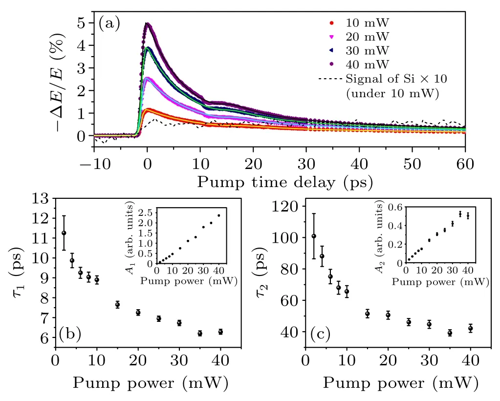
Fig.2.(a) The 1D TRTS of GeSn thin film and pure Si substrate under different pump power.The solid curves are the fitting results of Eq.(2).The signal of Si under a 10 mW pump is magnified by 10 times.Panels(b)and(c)are the fitting parameters under different pump power.
The 1D TRTS of GeSn film at different excitation powers is shown in Fig.2(a).It can be seen that after 2500 nm femtosecond laser excitation,the terahertz signal of GeSn film reaches its peak at around 1 ps and then begins the relaxation process.Due to the reflection of the pump light by the backside of substrate, a second excitation process appears at~13 ps.This entire process(including the rising edge of the signal)can be described by a formula containing two exponential relaxation processes(A1,τ1,A2,τ2)
wheret01(≈−1 ps from fitting) andt02(≈13 ps from fitting)are the pump excitation time and the secondary excitation time, respectively,tr1(≈1 ps from fitting) andtr2(≈4.5 ps from fitting)are the rise times of the signals during the two excitations,respectively.G(≈0.1 from fitting)is the secondary excitation coefficient, andCrepresents the relaxation process with lifetime much longer than our measurement range.Here we assume that the second excitation by the reflected pump can trigger the relaxation processes with similar lifetimes,which is good enough to get the trend of pump-powerdependence of the fitting parameters.We believe that such assumption is reasonable because the second peak is much smaller compared to the main peak, and it cannot change the trend of the fitting parameters.The fitting curve is shown in Fig.2(a),which can fit the secondary reflection excitation process well.
As shown in Fig.2(a),after 2500 nm femtosecond excitation,the terahertz signal of GeSn thin film reaches its peak at around 1 ps,and then starts the relaxation process.The amplitudes and relaxation time that describe the relaxation process are shown in Figs.2(b)and 2(c).The entire relaxation process is approximately in the order of 100 ps,and can be divided into a fast process(τ1)and a slow process(τ2).BothA1andA2are proportional to the excitation power,indicating that the power used has not yet reached the saturation absorption threshold.In addition,τ1andτ2both show a strong negative correlation to the excitation power, where the relaxation time will shorten at higher photo-generated carrier densities.Considering the semiconductor properties of the material, these two processes may be related to higher-order recombination processes of carriers, such as Auger recombination or radiative recombination.[17,18,32–36]
3.3.The 2D TRTS of GeSn thin film
We measure the time evolution of the transmitted terahertz electric field (2D TRTS) of GeSn after excitation with 15 mW pump power, as shown in Fig.3.The relative peak change of the transmitted terahertz electric field is about−2%,and it gradually decays with pump time delay.Using the data processing method of time-resolved terahertz time-domain spectroscopy,[18,24]we obtain the terahertz complex conductivity Δ ˜σ(ω)of GeSn film,as shown in Fig.3(c).In Fig.3(c),we list the Δ ˜σ(ω) at pump time delays of 0, 5 ps and 20 ps,which clearly shows its relaxation behavior with time delay.At delay time after photoexcitation, the real part of Δ ˜σ(ω)slowly increases with frequency, while the absolute value of the imaginary part shows a decreasing trend.This frequencydependent conductivity cannot be explained directly by the common Drude model, but can be well fitted by the Drude–Smith model[18,26]
Here,ε0is the vacuum permittivity,ε∞is the high-frequency dielectric constant of the sample,ωpis the plasma frequency,γis the scattering frequency, andcis a fitting parameter in the Drude–Smith model to describe backscattering.The fitting curve for the GeSn photoconductivity data is shown as the solid line in Fig.3(c).It can be seen that the fits are excellent,indicating that the carriers in the film after photoexcitation are different from the free carriers described in the Drude model,and exhibit some degree of localization(c/=0).This is generally caused by some defects in the crystal and can be observed in various semiconductor films.[26]

Fig.3.The 2D TRTS of GeSn.(a) Red curve is the THz electric field in the time-domain after passing through the sample.Blue curve is the transient change of THz electric field after pumping at τ =0 ps.(b)Transient change of THz electric field after pumping at selected pump time.(c)Extracted THz optical conductivity at selected pump time.

Fig.4.Parameters from Drude–Smith model fitting and some deduced parameters.(a)Plasma frequency ωp.(b)Photogenerated carrier density n.(c)Scattering rate γ.(d)MobilityµDS.
The parametersωpandγobtained by fitting with the Drude–Smith model as functions of pump-probe delay time are shown in Figs.4(a)and 4(c), respectively.We can calculate the photogenerated carrier densitynand mobilityµDSin the GeSn film using the following formula:[26]
wherem∗represents the effective mass of the carriers,eis the unit charge,andµDis the intrinsic mobility(without considering the contribution of backscattering due to defects).According to the previous studies, the effective mass of carriers in GeSn ism∗=0.02me,[33]thus the variations ofnandµDSwith pump-probe time delay can be obtained,as shown in Figs.4(b)and 4(d).
According to Fig.4,the mobility of photo-generated carriers is about 800 cm2·V−1·s−1, and reaches a minimum value at~15 ps after photoexcitation.However, the change of the scattering rate is not so significant,but the backscattering contribution caused by defects(measured by the parameterc)is more significant.Therefore,the main contribution to the change in the mobility of photo-generated carriers with pumpprobe delay time should come from the change of backscattering caused by the defects in the thin film.
Combining with the results of 1D TRTS on pump power dependence (dependence ofτ1andτ2on pump power), we speculate that Auger recombination may dominate the relaxation of terahertz signals.Therefore,we can use the rate equation to fit the carrier density[18]
wherek1andk2are the recombination rates of the first and second order processes.Here we only consider the first and second-order recombination processes,because the rate coefficient of higher-order recombination terms is 0 when included.The fitted curve is shown as the red solid line in Fig.4(b).We can see that the fitted curve agrees the experimental data very well, with the fitted parametersk1=(2.6±1.1)×10−2ps−1andk2=(6.6±1.8)×10−19cm3·ps−1.Generally speaking,in direct gap semiconductor materials, the first-order process comes from the capture of photo-generated carriers by defects,and the second-order process may come from defect-assisted Auger recombination[18]or radiative recombination.[35–37]However, in heavily-doped GeSn(direct bandgap), the radiative recombination mechanism can be excluded,since its lifetime at room temperature is much longer than our measurement range.[35–37]According to the recombination rate in the inset of Fig.4(b),we can see that the second-order recombination dominates before 20 ps,and the first-order recombination becomes the main recombination channel after 20 ps.
4.Discussion
According to the results of 1D and 2D TRTS of GeSn thin film under 2500 nm optical excitation, we can see that the excitation can generate photo-generated carriers in GeSn,which undergo a relaxation process with a timescale of about~100 ps.After the concentration of photo-generated carriers reaches its maximum, there are two relaxation channels: one is the Auger recombination process involving defect levels,which dominates before 20 ps;the other is the carrier capture process by defect levels,which dominates after 20 ps.During the entire recombination process, the carrier mobility is affected by defect scattering, causing a decrease of about 40%,reaching a minimum value of around~15 ps, and gradually relaxing to an equilibrium value.
In addition, we notice that the relaxation processes obtained from 1D and 2D TRTS are slightly different.The 1D data show two relaxation processes, with relaxation time of the orders of 10 ps and 50 ps, which cannot be fully correlated with the two carrier relaxation channels obtained from the 2D data.This is mainly because 1D data not only reflect the evolution of carrier concentration but are also affected by the transient change in carrier mobility,and therefore there are more factors included, leading to the difference observed by 1D and 2D TRTS.
Furthermore, during the relaxation of photo-generated carriers, they can diffuse simultaneously, and the diffusion lengthLDcan be calculated by the following formula:[26]
wherekBis the Boltzmann constant,Dis the diffusion constant at temperatureT, andkeffis the effective first-order recombination rate,which can be mathematically expressed as
The results are shown in Fig.5,where the diffusion lengthLDvaries slightly with the pump time,and the change ofLDwith respect to pump delay time is more pronounced when the concentration of photo-generated carriers is high (before 30 ps).The value ofLDis around 0.4µm,which is similar to previous research.[38]

Fig.5.Diffusion length of photogenerated carriers.
5.Conclusion and perspectives
We measure the time-resolved terahertz spectroscopy of GeSn thin film under 2500 nm laser excitation and study the ultrafast dynamics of its carriers.We find that there are two recombination channels: Auger process assisted by defects and defect capture,and the former dominates the carrier relaxation process within 20 ps after photoexcitation while the latter persists for a longer time.Meanwhile,we obtain the carrier diffusion length of GeSn,which is about 0.4µm.These results are important for the optoelectronic applications of GeSn semiconductors, and indicate that the minimum response time of this material can reach~100 ps,corresponding to a frequency upper limit of~10 GHz, making it a promising material for high-speed infrared detection.
Acknowledgments
Project supported by the National Natural Science Foundation of China(Grant Nos.12004067,11974070,62027807,and 52272137)and the National Key R&D Program of China(Grant No.2022YFA1403000).
猜你喜欢
课外语文·上(2023年2期)2023-03-11 10:06:08
——领悟张岱的“痴”
课外语文(2023年2期)2023-03-09 08:59:56
语文周报·教研版(2020年11期)2020-05-19 15:20:06
中学生百科·悦青春(2017年9期)2018-01-29 13:01:05
名作欣赏(2017年27期)2017-09-18 03:22:09
视野(2016年7期)2016-05-14 00:42:39
语文教学与研究(教研天地)(2015年6期)2015-06-03 02:16:33
茶博览(2015年12期)2015-03-09 06:49:50
海南热带海洋学院学报(2014年1期)2014-08-08 13:00:01
文学教育(2014年6期)2014-07-15 03:41:02

- Chinese Physics B的其它文章
- High responsivity photodetectors based on graphene/WSe2 heterostructure by photogating effect
- Progress and realization platforms of dynamic topological photonics
- Shape and diffusion instabilities of two non-spherical gas bubbles under ultrasonic conditions
- Stacking-dependent exchange bias in two-dimensional ferromagnetic/antiferromagnetic bilayers
- Controllable high Curie temperature through 5d transition metal atom doping in CrI3
- Tunable dispersion relations manipulated by strain in skyrmion-based magnonic crystals