
InGaAs/AlGaAs quantum well intermixing induced by Si impurities under multi-variable conditions
2023-12-01 05:50:28LIUCuicuiLINNanMAXiaoyuZHANGYuemingLIUSuping
中国光学 2023年6期
LIU Cui-cui,LIN Nan,MA Xiao-yu ,ZHANG Yue-ming,LIU Su-ping
(1.National Innovation Center of Radiation Application,China Institute of Atomic Energy, Beijing 102413, China;2.National Engineering Research Center for Optoelectronics Devices,Institute of Semiconductors, CAS, Beijing 100083, China;3.College of Materials Science and Opto-Electronic Technology, University of Chinese Academy of Sciences, Beijing 101408, China;4.Hitachi High-tech Scientific Solutions (Beijing) Co., Ltd., Beijing 100012, China)
Abstract: Catastrophic Optical Mirror Damage (COMD) on the cavity surface is the key factor limiting the threshold output power of high-power quantum well semiconductor laser diodes.To improve the output power of the laser diode,the band gap width of the active material in the cavity surface of the semiconductor laser diode can be adjusted by the quantum well intermixing technology to form a non-absorbing window transparent to the output laser.Based on the primary epitaxial wafers of InGaAs/AlGaAs high power quantum well semiconductor laser diode,using the single crystal Si dielectric layer grown by Metal Oxide Chemical Vapor Deposition (MOCVD) as the diffusion source,the research on Si impurity induced quantum well intermixing was carried out by using the Rapid Thermal Annealing (RTA) process.The effects of growth characteristics of Si dielectric layer,the temperature and time of RTA on the intermixing process were investigated.The experimental results show that the epitaxial 50 nm Si dielectric layer at 650 °C combined with 875 °C/90 s RTA treatment can obtain about 57 nm wavelength blue shift while maintaining the photoluminescence spectrum shape and the primary epitaxial wafers.It is found that the diffusion of Si impurities into the waveguide layer on the primary epitaxial wafer is the key to the remarkable effect of quantum well intermixing by the energy spectrum measurement technique.
Key words: semiconductor lasers;quantum well intermixing;rapid thermal annealing;blue shift;photoluminescence spectra
1 Introduction
In 1966,shortly after the advent of semiconductors,COOPERet al.[1]discovered that increasing the output power of GaAs homojunction semiconductor lasers to a certain level would result in Catastrophic Optical Damage (COD) and failure.In 1977,CHINONEet al.[2]discovered that an Al-GaAs/GaAs double heterojunction semiconductor laser operated continuously for a certain period resulted in Catastrophic Optical Mirror Damage (COMD)on its cavity surface.Using Scanning Electron Microscope (SEM) observation,it was found that high power density light output and cavity surface oxidation were important factors leading to its COMD[3].
For InGaAs/AlGaAs high-power Quantum Well(QW) semiconductor lasers,COMD suppression should start from its induced mechanism[4].According to test results,methods such as reducing non-radiative recombination at the cavity surface,suppressing light absorption of the cavity surface material,lowering the carrier concentration at the cavity surface,and improving the heat dissipation capacity at the cavity surface[5]can significantly suppress COMD.The preparation of non-absorbing windows based on Quantum Well Intermixing (QWI) technology is a low-cost and effective method to suppress the light absorption of cavity materials[6-7].Commonly used QWI methods include Impurity Induced Disordering (IID),Impurity Free Vacancy Induced Disordering (IFVD),Laser Induced Disordering (LID),etc.[8-11].Among them,in IID technique,a large number of point defects are induced by introducing impurities,and in combination with thermal annealing and other methods,the impurities and point defects are activated to obtain diffusion kinetic energy,ultimately causing changes in the composition and structure of quantum wells.In the 1980 s,LAIDIG[12]first found that QWI phenomenon occurred in AlAs/GaAs superlattice structures with the introduction of Zn impurities and heat treatment,and the heat treatment temperature in this method was only 575 °C,far below the temperature required for impurity free induced disordering.Until 1985,KALISKI[13]found that the effect of Si impurity inducing AlGaAs/GaAs superlattice QWI was better than that of other impurities.In 1987,MEIet al.[14]used Secondary Ion Mass Spectroscopy(SIMS) to test and found that the diffusion coefficient of Al atoms in AlGaAs materials increased significantly with the diffusion of Si impurities.Comprehensive research results show that Si impurities can form defect pairs with larger diffusion coefficients with Al atoms,and Si impurities can also increase the density of point defects in the QW system,thus effectively promoting the QWI of the AlAs/GaAs superlattice structure[6,15].
This paper presents a Non-Absorbing Window(NAW) preparation scheme for InGaAs/AlGaAs high-power QW semiconductor lasers using the method of Si impurity induced QWI.This method is based on the principle that the Si impurity is used as an induction source,which can efficiently induce the atomic interdiffusion between the materials in the QW and the materials in the barrier of the In-GaAs/AlGaAs semiconductor QW laser,eventually broadening the band gap of the active region material and suppressing its absorption of the self-generated laser.The preparation of NAW using the Si IID method not only reduces the optical absorption at the cavity surface of the laser,but also serves as an N-type doping element to form a non-carrier injection region at the cavity surface of the device,thus reducing the non-radiative composite here.This design does not require expensive equipment or complex processing,and can effectively increase the COMD threshold triggering power of the laser without changing its characteristic parameters.
2 Simulation analysis of QWI
2.1 Chip development and performance analysis
The primary epitaxial wafers of the InGaAs/Al-GaAs QW laser used in this paper were grown by Metal Oxide Chemical Vapor Deposition (MOCVD),with a reaction chamber growth temperature of 550-700 °C and a pressure of 5 kPa[16].The substrate is n-GaAs with a (100) plane offset [111]A-crystal-orientation of 15°.The schematic diagram of the ridge laser structure formed based on this primary epitaxial wafer is shown in Figure 1(color online).
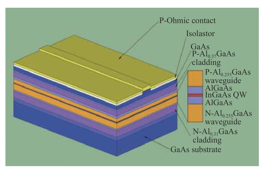
Fig.1 Epitaxial structure of InGaAs/AlGaAs QW laser diode图1 InGaAs/AlGaAs 量子阱激光器的外延结构
For In(1-x-y)GaxAlyAs quaternary compound semiconductor material,its band gap is shown in formula (1),so the increase of Al component will lead to the increase ofEg.Therefore,we determine whether QWI has occurred in the material by the central wavelength position.If a QWI occurs,it is proved that the Al component has entered the QWI material,and the band gap becomes wider,which is shown by the change of the luminescence wavelength toward the short wavelength,that is,the blue shift occurs.
Photoluminescence (PL) spectroscopy test is a commonly used method to obtain the central wavelength of lasers.The original PL test results of the primary epitaxial wafer of InGaAs/AlGaAs QW lasers in this paper are shown in Figure 2.According to the mapping scan results,the luminescence intensity is uniform,indicating that the composition of each layer of the epitaxial wafer is uniform.From the single-point PL signal peak,it can be seen that the peak center wavelength is 1 002.2 nm,and the Full Width at Half Maximum (FWHM) is about 23 nm.
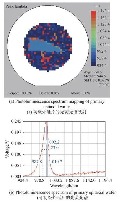
Fig.2 The PL spectrum of InGaAs/AlGaAs QW primary epitaxial wafer图2 InGaAs/AlGaAs 量子阱初级外延片的PL 谱测试结果
2.2 The effect of temperature on QWI
The existence of point defects in crystals leads to the breaking of the perfect arrangement rules of lattice atoms,changes the vibration frequency of atoms around the defects,increases entropy,and deteriorates the thermodynamic stability[4].By combining the diffusion coefficient equation of group III atomic point defects,it can be concluded that:
whereAis a function related to the vibration entropyS fand vacancy,Bis a function related to the vibration entropyS fand interstitial atoms,EIis the energy required to form a interstitial atom,f1andf2are constants,is the diffusion coefficient of Group III vacancies,is the diffusion coefficient of Group III interstitial atoms,KBis the Boltzmann constant,and its value is 1.38×10⁻²³J/K.Under the thermal equilibrium state,approximation can be considered as:A f1=Bf2,and2EV=E1,and the relationship curve between the relative interdiffusion coefficient of group III atoms and temperature can be fitted qualitatively according to formula (2),as shown in Figure 3.It can be seen that the diffusion coefficient of point defects in the group III-V material system is exponentially positively correlated with temperature,indicating that increasing the temperature is very beneficial for promoting the diffusion of point defects and enhancing the effect of QWI.
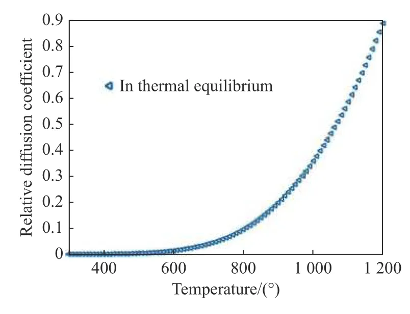
Fig.3 The relationship between relative interdiffusion coefficient and temperature图3 III 族原子相对互扩散系数与温度的关系
2.3 The effect of stress on QWI
At the interface of two materials with high lattice mismatch,there will be a certain amount of stress,which will cause compressive or tensile stress on the surface of the material.The surface compressive stress will cause the GaAs lattice atoms to be squeezed,and some atoms,especially Ga atoms,will be squeezed out of the interface,leaving a certain number of vacancy defects on the GaAs surface[17].To study the interface deformation during annealing process,the COMSOL multi-physical field modeling software was used to simulate the stress-strain behavior of GaAs with Si dielectric layers after annealing.
It is assumed that the epitaxial wafers are annealed at 850 °C,and stress is released when the annealing temperature drops to 200 °C,and finally stable deformation occurs at room temperature.The relevant parameters used in the calculation are shown in Table 1.The substrate material of the primary epitaxial wafer is 450 μm n-GaAs,the total thickness of the epitaxial wafer is approximately 4.5 μm,and both contain a large proportion of Ga and As components.To avoid calculation errors caused by excessive relative tolerance,the simulated substrate and epitaxial wafer are both 25-μm GaAs,with a dielectric layer of 200-nm Si.The simulation results based on COMSOL and magnified by 100 times are shown in Figure 4 (color online).It can be seen that the surface of GaAs undergoes compression caused by compressive stress after annealing,indicating that the Si dielectric layer will provide compressive stress to the GaAs surface and induce more Ga vacancies in GaAs,which is conducive to the QWI process.

Tab.1 Young's modulus,Poisson’s ratio,density and coefficient of thermal expansion of related materials表1 相关材料的杨氏模量、泊松比、密度及热膨胀系数
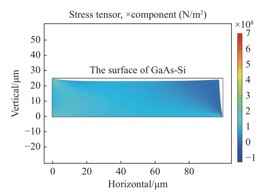
Fig.4 Deformation results of primary epitaxial wafer simulated by COMSOL after annealing图4 退火后初级外延片形变的COMSOL 模拟结果
3 Experiment and result analysis
3.1 Research on the effect factors of QWI
3.1.1 Effect of cover layer
During the annealing process,covering with GaAs cover plates not only reduces surface contamination,but also provides a certain pressure for As concentration,which can inhibit the decomposition and volatilization of As on the surface of the epitaxial wafer to some extent.The surface morphology of the primary epitaxial wafer at 875 °C/90 s RTA is shown in Figure 5 (color online).Figures 5(a) and 5 (b) show the surface morphology of primary epitaxial wafers with and without GaAs cover plates,respectively.Similar to the predicted results,the surface of epitaxial wafers with GaAs covers is smoother,and there are fewer ablative holes generated during annealing,indicating that the GaAs covers have a certain protective effect on the surface of the Si dielectric layer.Therefore,subsequent RTAs were conducted in the environment with GaAs covers.
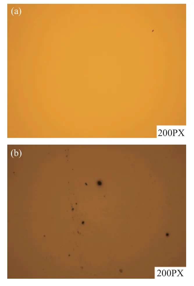
Fig.5 Surface morphology (a) with and (b) without epitaxial wafers after RTA图5 (a)有、(b)无盖片退火后外延片的表面形貌
3.1.2 The effect of temperature
The calculation results show that temperature has a significant effect on the diffusion coefficients of impurities and point defects.Therefore,the effect of temperature on QWI is investigated first.By using MOCVD,a 20-nm single crystal Si was grown on the surface of GaAs primary epitaxial wafers at the growth temperature of 800 °C.Then,a 90 s Rapid Thermal Annealing (RTA) was performed in the interval of 775 to 900 °C,and the PL results after annealing are shown in Figure 6 (color online).It can be seen that the effect of wavelength blue shift increases with the increase of heat treatment temperature.Compared to the original primary epitaxial wafers,a maximum wavelength blue shift of about 90 nm was obtained at 900 °C,but at this point,the FWHM was significantly widened and the waveform was severely deteriorated,indicating significant material damage.At 875 °C,the wavelength blue shift is about 57 nm,and the FWHM is well maintained.Therefore,it is believed that heat treatment at 875 °C can achieve a good QWI effect while also ensuring the lattice quality of the material.
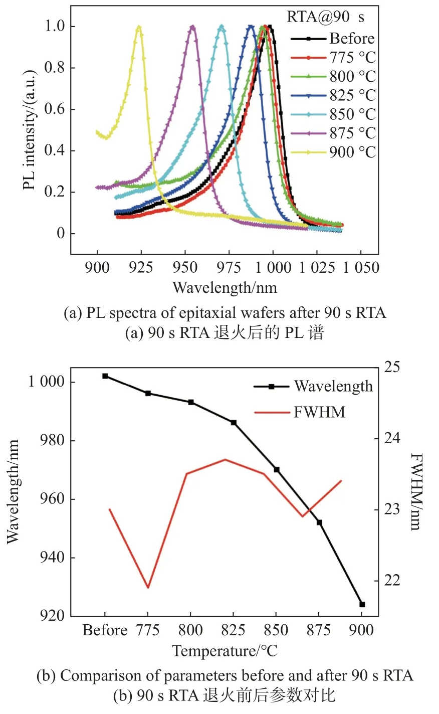
Fig.6 Effect of RTA temperature on wavelength blue shift of primary epitaxial wafers图6 RTA 温度对初级外延片波长蓝移的影响
3.1.3 The effect of heat treatment time
The effect of heat treatment time on QWI is further investigated.The annealing temperature is always 875 °C,and the annealing time is set to 60 s,90 s,and 120 s respectively.The PL results of the primary epitaxial wafers after annealing are shown in Figure 7 (color online).As the annealing time increases,the wavelength blue shift of the primary epitaxial wafer introducing Si impurities also gradually increases.However,when the annealing time reaches 120 s,the peak of the PL spectrum is already deformed.It indicates that after 90 s RTA treatment,a good blue shift effect can be achieved,and the peak intensity of the PL spectrum and the FWHM remain good.
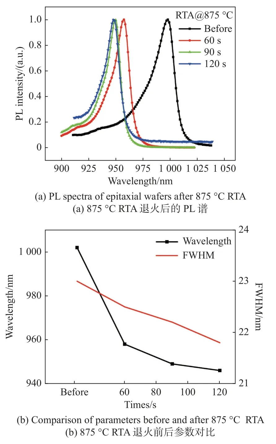
Fig.7 Effect of RTA time on wavelength blue shift of primary epitaxial wafers图7 RTA 时间对初级外延片波长蓝移的影响
3.1.4 The effect of the properties of the dielectric layer
If the Si grown on the epitaxial wafer surface is too thick,the lattice mismatch and the difference in coefficient of thermal expansion will be amplified,which will trigger the stress release during thermal annealing.The ability of a thinner Si layer to suppress the decomposition and outward volatilization of Ga and As atoms in the GaAs ohmic contact layer will also be weakened,so it is necessary to consider the effect of Si characteristics.The Si dielectric layer grown by MOCVD equipment is single crystal,and its lattice quality and density are affected by the reaction source,growth temperature and other conditions,so the Si dielectric layer grown under different conditions will also affect the QWI effect.Therefore,three types of Si epitaxial layers were prepared: 20 nm high-temperature Si grown at 800 °C,20 nm low-temperature Si grown at 650 °C,and 50 nm low-temperature Si,set as # 1,# 2,and # 3,respectively,to investigate the optimal growth conditions for Si dielectric layers that induce best QWI effect.
Similarly,a single RTA treatment at 875 °C/90 s was applied to the group of the primary epitaxial wafers,and the PL spectra of the primary epitaxial wafers were tested after heat treatment,as shown in Figure 8 (color online).It can be seen that the difference of QWI effect caused by the three types of Si layers is relatively small.For Si layers with the same thickness,the effect of Si layer growth temperature on wavelength blue shift is relatively small,but the FWHM is narrower for the high-temperature Si layers.For Si layers with the same growth conditions,thicker Si layers cause more wavelength blue shifts,reaching about 57 nm,but their FWHM is also larger,indicating that the material quality is greatly affected.
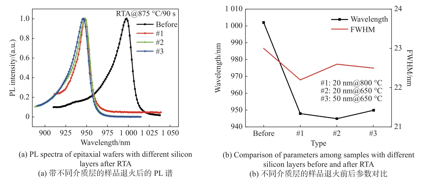
Fig.8 Effect of different silicon layers on wavelength blue shift of primary epitaxial wafers图8 Si 介质层对初级外延片波长蓝移的影响
3.2 Microscopic characterization of QWI effect
In order to accurately understand the diffusion depth of Si atoms,EDS was used to test the element distribution at different depths on the epitaxial wafer.The Si IID primary epitaxial wafers treated with 875 °C/90 s RTA were carried out Si layer removal treatment,and then corroded for 0 s,15 s,30 s,and 45 s using a special solution.The test results are shown in Figure 9 (color online).Experience shows that the corrosion rate of the corrosive solution is about 25-35 nm/s,so the surface of the etched epitaxial wafer corresponds to different depths.From the EDS results,it can be seen that the p-type doping element of the primary epitaxial wafer is C,so the element C content is ligher when the surface layer of GaAs is not corroded moreover,the element Si content is also higher,and The content of both in the same order of magnitude;with the corrosion time increases to 15 s,the element C content gradually decreases,and the element Si content decreases significantly;when the corrosion time reaches 30 s,i.e.,when the corrosion depth reaches approximately the upper limiting layer,the Si content has decreased to 22.2% of the original Si content in the surface layer;when the corrosion time further increases to 45 s,i.e.,when the corrosion depth reaches approximately the upper waveguide layer or near the QW region,the Si content basically decreases to 0.This result shows that the Si impurities can diffuse into the upper waveguide layer of the primary epitaxial wafer after 875 °C/90 s RTA treatment,and then produce an effective QWI induction effect.
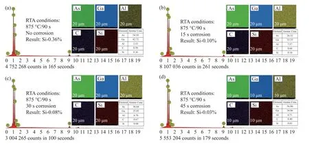
Fig.9 Surface EDS results of element composition at different corrosion times of primary epitaxial wafers after 875 °C/90 s RTA.(a) Untreated sammple;(b) corrosion for 15 s;(c) corrosion for 30 s;(d) corrosion for 45 s图9 EDS 测试875 °C/90 s RTA 处理后初级外延片不同腐蚀时长的元素组成。(a)未处理样品;(b)腐蚀15 s;(c)腐蚀30 s;(d)腐蚀45 s
4 Conclusion
In order to comprehensively improve the performance index of InGaAs/AlGaAs semiconductor QW lasers,a feasible scheme for Si impurity induced QWI is investigated in this paper.The relationship between the effect of Si impurity-induced QWI and the nature of dielectric layer and heat treatment conditions was investigated by using the variable-controlling method with multiple sets of control conditions.The PL test results show that growing a 50 nm Si epitaxial dielectric layer at 650 °C
——中文对照版——
1 引言
半导体问世不久的1966 年,COOPER 等人[1]in combination with 875 °C/90 s RTA heat treatment results in a wavelength blue shift of about 57 nm.Combined with EDS test,it is found that Si impurity atoms can diffuse into the upper waveguide layer or QW of the InGaAs/AlGaAs semiconductor QW laser primary epitaxial layer after 875 °C/90 s RTA,resulting in a significant QWI effect.In the future,Si impurity induced QWI NAW can be prepared by combining epitaxial growth technology and RTA technology to suppress CODs and continuously improve the output power of InGaAs/Al-GaAs semiconductor QW lasers.发现,当GaAs 同质结半导体激光器的输出功率升高到一定值时便会产生光学灾变损伤(Catastrophic Optical Damage,COD)并失效。1977 年,CHINONE 等人[2]发现AlGaAs/GaAs 双异质结半导体激光器连续工作一定时间后,在其腔面处将产生了腔面光学灾变损伤(Catastrophic Optical Mirror Damage,COMD)。使用扫描电子显微镜(Scanning Electron Microscope,SEM)观测发现,高功率密度光输出及腔面氧化是导致其发生COMD 的重要因素[3]。
对于InGaAs/AlGaAs 高功率量子阱(Quantum Well,QW)半导体激光器,抑制COMD 应从研究其诱发机理入手[4]。经检验,通过减少腔面处的非辐射复合、抑制腔面材料的光吸收、降低腔面处载流子浓度、提高腔面处散热能力等方法[5],均可显著抑制COMD。基于量子阱混杂(Quantum Well Intermixing,QWI)制备非吸收窗口是一种成本较低、效果显著的抑制腔面材料光吸收的方法[6-7]。常用的量子阱混杂方法包括杂质诱导量子阱混杂(Impurity Induced Disordering,IID)、无杂质诱导量子阱混杂(Impurity Free Vacancy Induced Disordering,IFVD)、激光诱导量子阱混杂(Laser Induced Disordering,LID)等[8-11]。其中,IID 技术是通过引入杂质诱生大量点缺陷,并结合热退火等工艺使杂质及点缺陷激活并获得扩散的动能,最终造成量子阱组分及结构的变化。上世纪80 年代,LAIDIG[12]最先发现引入Zn 杂质并经热处理的AlAs/GaAs 超晶格结构发生了量子阱混杂现象,且此方法中的热处理温度仅575 °C,远低于无杂质诱导混杂所需温度。直到1985 年,KALISKI[13]发现Si 杂质诱导AlGaAs/GaAs 超晶格量子阱混杂的效果比其他杂质更好。1987 年,MEI 等人[14]利用二次离子质谱(Secondary Ion Mass Spectrometry,SIMS)测试发现在AlGaAs 材料中Al 原子的扩散系数会随着Si 杂质的扩散显著上升。综合研究认为,Si 杂质能与Al 原子形成扩散系数较大的缺陷对,且Si 杂质也可增加量子阱体系中点缺陷的密度,进而有效促进AlAs/GaAs 超晶格结构的量子阱混杂[6-15]。
本文利用Si 杂质诱导量子阱混杂的方法为通过InGaAs/AlGaAs 高功率量子阱半导体激光器提供非吸收窗口(Non-Absorption Window,NAW)。主要原理是采用Si 杂质作为诱导源,高效地诱导InGaAs/AlGaAs 半导体量子阱激光器的量子阱区材料与垒区材料发生原子互扩散,最终使有源区材料禁带宽度变宽,抑制其对自身产生的激光的吸收。利用Si 杂质诱导量子混杂方法制备非吸收窗口不仅可以减少激光器腔面处的光吸收,也可以作为N 型掺杂元素在器件腔面处形成非载流子注入区,减少此处的非辐射复合。这种设计不需高成本的设备或复杂的处理过程,在不改变激光器特征参数的同时,可有效提高其COMD 阈值触发功率。
2 量子阱混杂的模拟分析
2.1 芯片研制及性能分析
本文所使用的InGaAs/AlGaAs 量子阱激光器初级外延片采用金属氧化物化学气相沉积(Metal Oxide Chemical Vapor Deposition,MOCVD)生长,反应室生长温度为550~700 °C,反应室压强为5 kPa[16]。衬底为(100)面偏[111]A 晶向15°的 n-GaAs,基于该初级外延片形成的脊型激光器结构示意图如图1 所示。
对于In(1-x-y)GaxAlyAs 四元化合物半导体材料,其禁带宽度如公式(1)所示,故Al 组分增多会导致Eg增大。因此,本研究通过中心波长位置判定材料是否发生了量子阱混杂。若发生了量子阱混杂,证明量子阱材料中有了Al 组分,禁带宽度变宽,表现为发光波长朝短波长变化,即蓝移。
光致发光(Photoluminescence,PL)光谱测试是获得激光器中心波长的常用方法,本文中In-GaAs/AlGaAs 量子阱激光器初级外延片的原始PL 测试结果如图2。由其映射扫描结果可知其发光强度均匀。说明外延片各层成分均匀。由单点PL 信号峰可知峰值中心波长为1 002.2 nm,半高全宽(Full Width at Half Maximum,FWHM)约为23 nm。
2.2 温度对量子阱混杂的影响
晶体中点缺陷的存在导致晶格原子的完美排列规则被打破,缺陷周围的原子振动频率发生改变,熵值增大,热力学稳定性变差[4]。结合III 族原子点缺陷互扩散系数方程可得:
其中,A是与振动熵S f及空位相关的函数,B是与振动熵S f及填隙原子相关的函数,EI为形成一个填隙原子所需要的能量,f1、f2是常数,是III族空位的扩散系数,是III 族间隙原子的扩散系数,KB为玻尔兹曼常数,其值为 1.38×10⁻²³J/K。热平衡状态下可考虑存在以下近似:A f1=Bf2,2EV=E1。根据公式(2)定性拟合出III 族原子相对互扩散系数与温度的关系曲线,如图3 所示。可见,III-V 族材料体系内点缺陷的扩散系数与温度呈指数型正相关。证明升高温度非常有利于促进点缺陷的扩散,提升量子阱混杂的效果。
2.3 应力对量子阱混杂的影响
在两种晶格失配度较大的材料界面处会存在一定应力,从而使材料表面存在压应力或张应力。而表面压应力会使GaAs 晶格原子受到挤压,部分原子,尤其是Ga 原子会被挤压出界面而在GaAs 表面留下一定数量的空位缺陷[17]。为了研究退火过程中的界面形变,使用COMSOL 多物理场建模软件模拟了带有Si 介质层的GaAs 退火后的应力应变情况。
假设外延片经过850 °C 高温退火,在退火温度降到200 °C 时产生应力释放,并最终在室温下产生稳定形变,计算使用的相关参数见表1。初级外延片衬底材料为450 μm 的n-GaAs,外延片总厚度约为4.5 μm,且均含大比例Ga、As 组分。为避免相对容差过大产生的计算错误,选用衬底及外延片为25 μm GaAs,介质层为200 nm Si 用于模拟分析。基于COMSOL 并放大100 倍后的模拟结果如图4(彩图见期刊电子版)所示。可见,退火后GaAs 表面出现了由压应力带来的缩紧现象,这表明Si 介质层会为GaAs 表面提供压应力,诱导GaAs 内产生更多Ga 空位,这有利于量子阱混杂过程的进行。
3 实验及结果分析
3.1 量子阱混杂的影响因素研究
3.1.1 盖片层的影响
在热退火过程中,加盖GaAs 盖片不仅能减少表面沾污,还能提供一定浓度As 压。这可在一定程度上抑制外延片表面As 的分解及挥发。经875 °C/90 s RTA 退火后的初级外延片表面形貌见图5(彩图见期刊电子版)。图5(a)、5(b)分别为有、无GaAs 盖片的初级外延片表面形貌。与预测结果相同,有GaAs 盖片的外延片表面更加光洁。这是因为退火产生的烧蚀孔较少。说明GaAs 盖片对Si 介质层表面起到了一定的保护作用,故后续RTA 均在有GaAs 盖片环境下进行。
3.1.2 温度的影响
由计算可知,温度对杂质及点缺陷的扩散系数影响极大,故首先研究温度对量子阱混杂的影响。利用MOCVD 在初级外延片GaAs 表面生长20 nm 单晶Si,生长温度为800 °C。然后,在775~900 °C 区间进行90 s 快速热退火(Rapid Treatment Annealing,RTA)处理,退火后的PL 结果如图6(彩图见期刊电子版)所示。可见,波长蓝移的效果随热处理温度升高而增大。对比原始初级外延片,在900 °C 时获得约90 nm 的最大波长蓝移量,但此时FWHM 显著加宽,波形严重恶化,说明材料损伤较大。而在875 °C 时波长蓝移量约为57 nm,且FWHM 保持较好。故认为875 °C热处理温度可在获得良好量子阱混杂效果的同时保证材料的晶格质量。
3.1.3 热处理时间的影响
继续研究热处理时间对量子阱混杂的影响。退火温度均为875 °C,退火时间分别设为60s、90s、120s,退火后初级外延片的PL 结果如图7(彩图见期刊电子版)所示。可见,随着退火时间延长,引入Si 杂质的初级外延片波长蓝移也逐渐增加,但退火时间达到120s 时PL 谱峰已经变形。图7 表明经90s RTA 处理可获得较好的蓝移效果,PL 谱峰值强度、FWHM 均保持较好。
3.1.4 介质层性质的影响
如果外延片表面生长的Si 过厚,则晶格失配及热膨胀系数的差别会被放大,会触发热退火过程中的应力释放。而较薄的Si 层抑制GaAs 欧姆接触层中Ga、As 原子分解和向外挥发的能力也会减弱,因此需要考虑Si 特性的影响。MOCVD设备所生长的Si 介质层为单晶材料,其晶格质量和致密度受到反应源、生长温度等条件的影响,故不同条件下生长的Si 介质层也会影响量子阱混杂效果。因此,制备了3 种Si 外延层:800 °C下生长的20 nm 高温Si、650 °C 下生长的20 nm-Si 和50 nm 低温Si,分别设为#1,#2,#3,用于寻找诱导量子阱混杂效果最佳的Si 介质层生长条件。
同样,对该组初级外延片进行875 °C/90 s 单次RTA 处理,并在热处理后测试初级外延片的PL 谱,见图8(彩图见期刊电子版)。可见,3 种类型的Si 层所引起的量子阱混杂效果差别较小。结果表明对于厚度相同的Si 层,Si 层生长温度对波长蓝移量的影响较小,但带有高温Si 层的FWHM 更窄。对于生长条件相同的Si 层,较厚的Si 层所引起的波长蓝移更多,达到了57 nm 左右,但此时其FWHM 也较大,说明材料质量受影响较大。
3.2 量子阱混杂效果的微观表征
为了更准确地了解Si 原子的扩散深度,使用EDS 测试了外延片不同深度处的元素分布。先对875 °C/90 s RTA 处理的Si IID 初级外延片进行去Si 层处理,再使用特制溶液分别腐蚀0 s、15 s、30 s、45 s,测试结果见图9(彩图见期刊电子版)。经验表明:腐蚀液的腐蚀速度约为25~35 nm/s,腐蚀后的外延片表面对应不同深度的区域。由EDS 结果可见,该初级外延片的p 型掺杂元素为C,故表层GaAs 未被腐蚀时C 元素含量较高,而Si 元素的含量也较高,且二者的含量在同一量级;随腐蚀时间增加至15 s,C 元素含量逐渐减少,Si 元素含量则大幅度下降;当腐蚀时间为30 s,约腐蚀到上限制层时,Si 含量已下降至表层的22.2%;当腐蚀时间为45 s 时,约腐蚀到上波导层或接近量子阱区,此时Si 含量基本下降为0。该结果证明了经875 °C/90 s RTA 处理,Si 杂质可以扩散到初级外延片的上波导层区,进而产生有效的量子阱混杂诱导效果。
4 结论
为了全方面提高InGaAs/AlGaAs 半导体量子阱激光器的性能指数,本文研究了Si 杂质诱导量子阱混杂的可行方案。利用控制变量法,设置了多组对照条件,研究了Si 杂质诱导量子阱混杂 效果与介质层性质、热处理条件等因素的关系。PL 测试结果显示,在650 °C 下生长50 nm Si 外 延介质层结合875 °C/90 s RTA 热处理,可获得 约57 nm 的波长蓝移量。结合EDS 测试发现,875 °C/90 s RTA 后Si 杂质原子可扩散到In-GaAs/AlGaAs 半导体量子阱激光器初级外延片 的上波导层或量子阱,因而产生显著的量子阱混 杂效果。未来,可结合外延生长技术、RTA 技术 制备Si 杂质诱导量子阱混杂非吸收窗口,抑制光 学灾变发生,持续提升InGaAs/AlGaAs 半导体量 子阱激光器的输出功率。
猜你喜欢
原子与分子物理学报(2021年1期)2021-03-29 07:29:36
疯狂英语·爱英语(2020年6期)2020-07-04 03:03:25
疯狂英语·新策略(2020年6期)2020-06-28 04:54:18
原子与分子物理学报(2020年5期)2020-03-17 07:00:26
原子能科学技术(2019年6期)2019-06-14 03:58:30
中国劳动关系学院学报(2016年3期)2016-09-26 01:58:19
意林(2016年13期)2016-08-18 22:38:36
唐山文学(2016年11期)2016-03-20 15:25:49
电脑知识与技术(2014年9期)2014-05-30 07:35:23
物理化学学报(2012年2期)2012-12-05 02:27:46

- 中国光学的其它文章
- 惯性传感器地面弱力测量系统热设计
- Orbital-angular-momentum spectra in coherent optical vortex beam arrays with hybrid states of polarization
- The influence of the number of coupling regions on the output of the ding-shaped microring resonator
- A sliding-mode control of a Dual-PMSMs synchronization driving method
- Polarization-multiplexing of a laser based on a bulk Yb:CALGO crystal
- Compact voice coil deformable mirror with high wavefront fitting precision