Model and data of optically controlled tunable capacitor in silicon single-photon avalanche diode
Mei-Ling Zeng(曾美玲), Yang Wang(汪洋), Xiang-Liang Jin(金湘亮),†, Yan Peng(彭艳), and Jun Luo(罗均)
1School of Physics and Electronics,Hunan Normal University,Changsha 410081,China
2School of Mechatronic Engineering and Automation,Shanghai University,Shanghai 200444,China
Keywords: photocapacitance effect,single-photon avalanche diode,interfacial traps
1.Introduction
As a core device in the field of extremely weak light detection, single-photon avalanche diodes (SPADs) fabricated based on the complementary metal–oxide–semiconductor(CMOS) process have been proven to have the advantages of high signal-to-noise ratio, high temporal resolution, and high dynamic range.[1–5]With the continuous development and optimization of image sensing technology, it is possible to manufacture millions of pixels with single-photon detection capability on a single chip.[6]To date, a great deal of research has been conducted to develop SPAD devices with high performance; for example, back-illuminated three-bit stacked SPADs with extremely low tunnel noise and high photon detection probability,[7]SPAD devices with improved photon detection probability by designing antireflection nanostructures,[8]near-infrared enhanced singlephoton detectors,[9,10]et al.With the development of semiconductor technology, semiconductor devices face increasing stability and reliability problems, among which capacitance is an important factor affecting the response speed of the device.However,there are few studies on the capacitance characteristics of SPADs at present, and the research directions mainly focus on broadening the spectral response range, improving the photon detection probability, and optimizing the dark count.[11–19]As a diode, an SPAD exhibits capacitive characteristics in addition to resistive effects when an AC voltage is applied.When forward and reverse voltages are applied across the diode,the diffusion capacitance and barrier capacitance exist respectively.Ideally,both capacitances are derived from the free carrier motion of the device itself.However, in the actual silicon planar process, there are charge traps at the interface between silicon and silicon dioxide.These traps are likely to exchange charges with free carriers,which affect the density of carriers in the surface layer of the device, thereby causing capacitance influence.Does this indicate some kind of correlation between the interfacial traps of the semiconductor and the capacitance? A long time ago,the literature[20]reported that the existence of traps in the semiconductor bandgap caused the photocapacitance effect.In the literature,the photocapacitance measurement of GaP materials was used to determine the energy level and concentration of deep traps in the material.In 1997,Tanet al.studied the interface properties of SiO2/SiC through the capacitance–voltage(C–V)method and proposed a formula for calculating the average density of interface defect states.[21]Maet al.analyzed the optical power dependence of capacitance by establishing a differential capacitance model for a single-row carrier photodetector,to optimize the high-speed performance of the detector at different optical powers.[22]Sengougaet al.studied theC–Vcharacteristics of two P-type silicon-doped GaAs Schottky diodes and observed that the deviation of theC–Vcharacteristics was related to the deep body defects with non-uniform density.[23]Reference[24]reported the photocapacitance effect in organic heterojunction devices constituting a PN junction, attributing the photocapacitance effect to charge traps.It can be seen that in semiconductor devices,the capacitance is closely related to the deep trap center of the photocapacitance effect in particular.
In this work, the capacitive properties of SPADs fabricated in a silicon-based process are investigated,and the photocapacitance effect is also reported.Through a small-signalC–Vtest at room temperature and low frequencies,the capacitance of SPAD devices under light is significantly higher than under no light.As the frequency increases,the gap gradually narrows.We believe this difference in capacitance is related to interfacial traps in the samples.
2.Device structure and capacitance analysis
Silicon is easily oxidized to form high-quality silicon dioxide,which allows silicon dioxide to be used as a diffusion mask during device fabrication and as an insulating material for many devices.Figure 1 is a cross-sectional view of the circular single-photon avalanche diode structure designed in this paper, and figure 2 shows the layout of the device (left)and the microscope image of the device based on the 0.18µm standard bipolar-CMOS-DMOS(BCD)process(right).In the fabrication of SPAD devices based on standard silicon technology, a layer of 0.01 µm–0.1 µm silicon dioxide is first thermally grown on a flat P-type silicon wafer as a diffusion mask layer.Next,photolithography is performed on the oxide layer,and the shallow trench isolation(STI)regions are etched and deposited with silicon dioxide.According to the specific structure of the device,multiple photolithography and implantation of high-energy phosphorus ions and boron ions are performed to form a photosensitive PN junction with a diameter of 20µm.After this,an aluminum electrode is formed on the surface of the silicon wafer by reactive sputtering to connect the device to the outside.This work adopts the dual diode structure of a P+/N-well and deep N-well/P substrate.Among them, the P+/N-well can form a high field multiplication region as a photosensitive junction.The deep N-well/P substrate acts as an isolation diode,preventing the photo-generated carriers of the substrate from entering the photosensitive junction and causing charge crosstalk.A P-well guard ring at the edge of the PN junction prevents premature edge breakdown of the device.
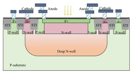
Fig.1.Single-photon avalanche diode(SPAD)structure.
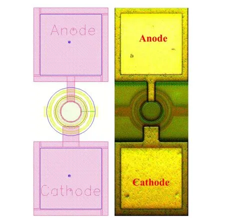
Fig.2.Layout and microscope images of SPAD devices.
SPADs need to work in a reverse-biased state, i.e., the cathode is connected to a high potential, and the anode is grounded.The two-dimensional simulation of the device is carried out in a technology computer-aided design (TCAD)simulator to obtain the electric field distribution at each position of the device in Geiger mode,as shown in Fig.3.Due to the different doping concentrations,the widths of the depletion regions of the P+/N-well,P-well/N-well,and P-well/deep Nwell junctions are different.When the device is reverse biased,the PN junction is equivalent to a large resistance and the voltage drop mainly exists in the depletion region,so the width of the depletion region can be observed through the electric field distribution.The simulation results show that the electric field strength of the central P+/N-well junction is the largest,so the avalanche breakdown is concentrated in the central P+/N-well junction and the device works normally.According to Shockley’s theory,the diode barrier capacitance can be expressed as
whereεrandε0are the relative permittivity of silicon (11.9)and the vacuum permittivity (8.854×10⁻¹²F/m),Ais the cross-sectional area of the junction, andWis the width of the depletion region of the PN junction.The electric field affects the widthWof the depletion region, and the equivalent capacitance distribution in the SPAD device in Fig.4 can be obtained from the electric field distribution.C1is the capacitance of the photosensitive PN junction.C2,C3are the side junction capacitances of the guard ring/N-well,andC4is the guard ring/deep N-well junction capacitance.The parasitic capacitance between the deep N-well and the substrate is independent of the capacitance between the cathode and anode, so it is not indicated in the figure.The total capacitance when the SPAD device is reverse biased can be expressed asCSPAD=C1+C2+C3+C4.Equation (1) introduces the relationship between the capacitance and the width of the depletion region.During the electrostatic analysis of the abrupt junction,it is found that the dependence ofWand the bias voltage varies with the impurity distribution.The specific formula is
whereqis the electronic charge (1.6×10⁻¹⁹C),NBis the impurity concentration on the lightly doped side,Vbiis the junction potential, andVRis the applied reverse bias voltage.Equation(2)can be substituted into Eq.(1)to get
It can be seen from Eq.(3) that the barrier capacitance is related to the junction area and impurity concentration.
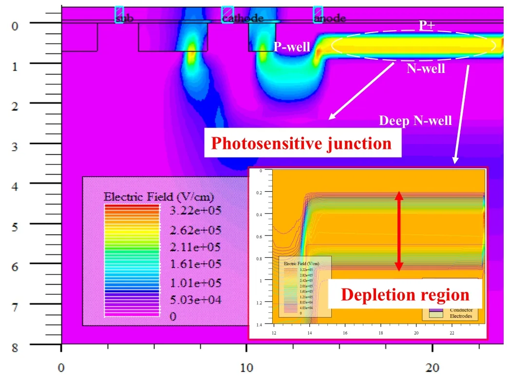
Fig.3.Electric field distribution of the SPAD device operating in Geiger mode.
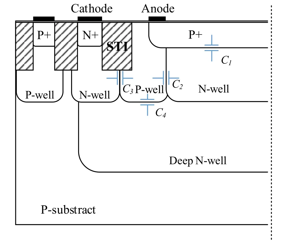
Fig.4.Equivalent capacitance distribution of the SPAD device.
However, for silicon-based photodetectors, illumination can affect the carrier concentration inside the device.It can be expressed as the following process: when a photon with energy exceeding the silicon bandgap(1.12 eV)irradiates the device,it can excite an electron from the valence band to the conduction band and leave a hole in the valence band.Electron–hole pairs move directionally in an electric field to form an electric current.Thus illumination increases the free carrier concentration inside the SPAD.The specific concentration of photo-generated carriers per unit time can be expressed asNLight=∆I/(qv),where ∆Iis the difference between the current and the dark current of the device under illumination,andvis the semiconductor volume.Figure 5 shows the current–voltage (I–V) characteristic curves of the SPAD device designed in this paper tested in light and dark environments(data from the previous work on this subject;see Ref.[25]).As can be seen from the figure,when the SPAD works in linear mode,the photocurrent is several tens of nanoamps higher than the dark current.Therefore, we should modify the capacitance formula to account for the effects of light and dark conditions on the device.We define Eq.(3) as the barrier capacitance under a no-light environment and Eq.(4)as the barrier capacitance under illumination,
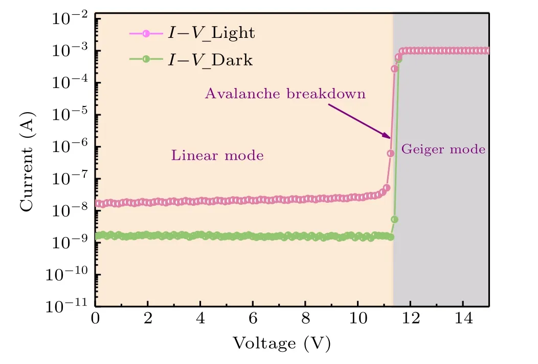
Fig.5.The I–V characteristic curves of the SPAD in light and no-light environments.
3.Test and discussion
With a SPAD in reverse bias,when the AC signalvis superimposed on the DC bias, the total voltage drop across the junction isVbias+v.Whenvis at a positive voltage, the AC signal slightly reduces the reverse bias on the junction,i.e.,the charge on both sides of the depletion region is reduced.Whenvchanges in reverse, the total reverse bias voltage across the junction increases immediately,causing an increase in charge on both sides of the junction.The effect of the AC signal can be seen as a small fluctuation of the charge density around its steady-state value.Due to the small magnitude ofv, the displacement of the fluctuating charge at the depletion layer boundary is almost negligible.The alternating increase and decrease of positive and negative charges at the edge of the SPAD depletion region are similar to the principle of physical plate capacitors, and the experiments in this paper are based on this principle to measure the capacitance characteristics of SPAD devices.The test instrument adopts the B1505A system of a power device analysis instrument,which has a touchable liquid crystal display screen for setting parameters, data display,and data processing.The test process is to put the device into the probe box, with the metal probes in contact with the cathode and anode of the SPAD,and superimpose a small sinusoidal signal with an amplitude of 100 mV and adjustable frequency on the DC reverse bias voltage of the device.To measure the photocapacitive effect, the device capacitance is measured in two cases.First,the test box is closed and a dark environment is maintained to measure the dark capacitance of the device.Second,the device’s photocapacitance is measured given a single light source.
Silicon-based SPAD devices can only respond to visible light,so this test uses red,orange,green,and blue light as light sources and the measured capacitance is represented byCred,Corange,Cgreen, andCblue, respectively, with the dark capacitance represented byCdark.The bias voltage of the device is from 0 V to 5 V,and theC–Vtest results are shown in Fig.6.
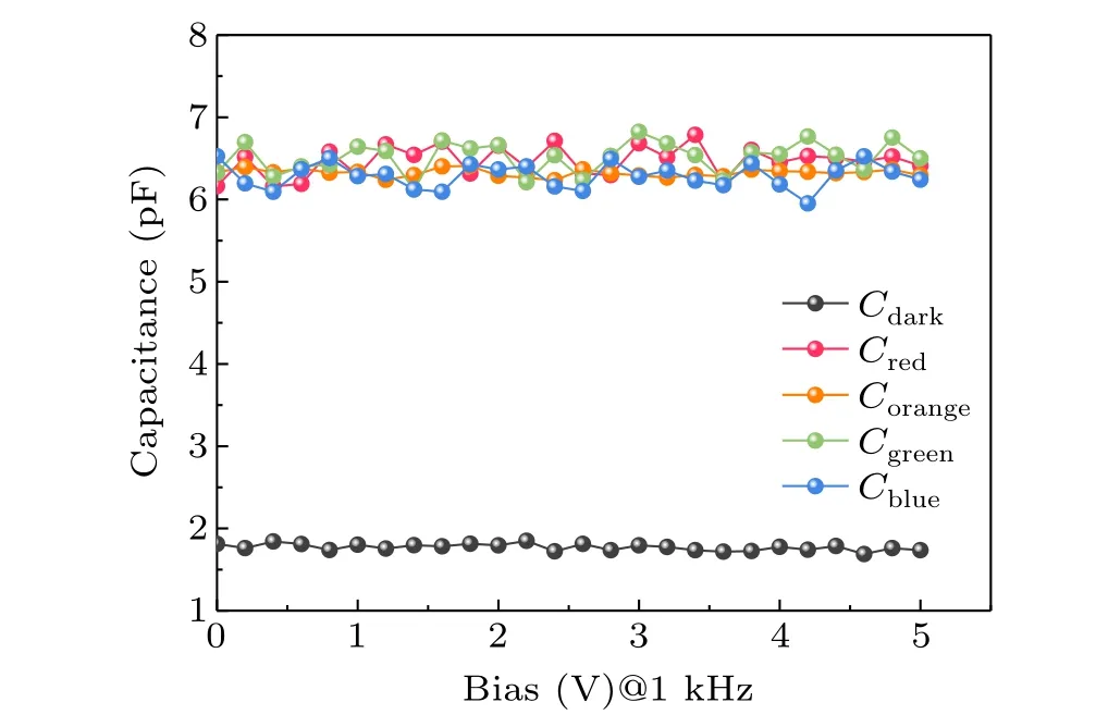
Fig.6.The C–V curves of the device with and without light at 1 kHz frequency.
As can be seen from the figure, the dark capacitance of the device is around 1.8 pF and the photocapacitance generally fluctuates around 6.3 pF.Moreover,the wavelength of the light source has little effect on the capacitance of the device,which can be ignored.∆C=Clight−Cdark≈4.5 pF,indicating that light can increase the junction capacitance of the device,because light excites photo-generated electron–hole pairs and increases the carrier concentration.The width of the depletion layer of the PN junction swings around the stable value with a small AC signal,which enables the carriers to respond in time to the AC signal.In silicon-based semiconductor devices,the response time of the majority carrier is in the range of 10−10s or less,indicating that the device can respond to very high signal frequencies.Therefore,we extended our research scope to study the frequency dependence of the capacitance of SPAD devices.
Figure 7 shows the capacitance variation curves of SPAD devices at frequencies from 1 kHz to 5 MHz.Among them,the blue curves represent capacitance versus voltage measured under a single blue light source at different frequencies.The black curves represent capacitance versus voltage measured in dark conditions at various frequencies,and the additionally marked small graphs show details of the dark capacitance.The figure shows that under the same bias voltage,the dark capacitance of the device remains almost unchanged with increasing frequency.However, with increasing frequency, the photocapacitance decreases significantly.We obtain the preliminary conclusion that the photocapacitance of SPAD increases at low frequencies and decreases at high frequencies.According to Eq.(4), the difference between the dark capacitance and the photocapacitance is caused by the change in the carrier concentration, and the changing trend of the capacitance should be consistent at different frequencies.However,there are differences in the actual test results.
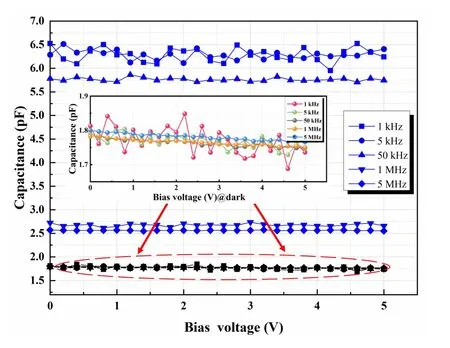
Fig.7.The C–V curves of dark capacitance and photocapacitance at different frequencies.
In Ref.[23], the authors observed the frequency dependence of capacitance in different types of deep-level traps,which was also observed in organic heterojunction devices in Ref.[24].The silicon-based SPAD devices fabricated by the planar process all contained the Si–SiO2system,and it is obvious that the movement space of the carriers was mainly in the surface layer of the silicon wafer.With the development of the manufacturing process,the quality and performance of the device have been greatly improved.However,additional charges and traps are still introduced in the Si–SiO2structure.Since the charge distribution is closely linked to the occurrence of vacancies,traps play an important role in the electron transport properties.For example,an SPAD with STI as the guard ring introduces huge noise to the device,[26]because there are many trap states in the STI region filled with SiO2, which trap and release the carriers in the device and increase the after-pulse.Therefore, we attribute this effect of SPAD photocapacitance to the interfacial traps of the Si–SiO2system, which can explain the photocapacitance versus frequency in Fig.7.When the device receives photons with energy greater than the band gap, electrons in the valence band absorb the energy of the photons and are excited into the conduction band to become free electrons.The concentration of photocarriers in light is far greater than that under dark conditions, and the photocapacitance is greater than the dark capacitance.
Next,the effect of interface traps on photocapacitance is considered.First of all,the interface trap is mainly due to the formation of a“dangling bond”between Si and SiO2(that is,the silicon atom has an atomic bond in a dangling state), or the oxygen atom at the interface is not connected to the silicon atom,but is in an interstitial position or missing.Interface traps introduce energy levels in the forbidden band of the Si–SiO2interface(which generally can be distributed in the whole forbidden band range),and these traps can trap both electrons and holes.If the energy level is electrically neutral when occupied by electrons and positively charged after releasing electrons, it is called a donor interface state; if the energy level is negatively charged after accepting electrons, it is called an acceptor interface state.In semiconductor silicon, the typical response time of the majority carrier is 10−10s or less,so when making capacitance measurements,the majority of the carrier can flow in and out quickly, so the carrier can respond to the AC signal promptly.However, the time constant of the interface state is large and decreases exponentially as the value ofEF−Eiincreases.Therefore, interface traps cannot respond to high-frequency signals.Assuming that the interface state is a donor state, when the device receives a photon, the energy of the electron in the trap absorbs the photon transitions from the forbidden band to the conduction band, thereby affecting the charge distribution inside the device.These trap states are charged and discharged as the bias voltage changes.In the frequency range below 1 MHz,the charge and discharge of the interface traps can follow the low-frequency signal, so the medium photocapacitor includes the trap capacitance,and the change of the total photocapacitance follows the law;that is,it decreases with increasing frequency.After the frequency continues to increase, the interface traps do not respond and do not charge and discharge, so the capacitance at frequencies above 1 MHz is significantly reduced.Since there are no trap states involved, there is only a small change in capacitance from 1 MHz to 5 MHz.The interface state density is an important criterion to measure the quality of the Si–SiO2interface.The interface state density represents the interface defect density per unit area and unit energy(number of defects×cm−2·eV−1):
In the formula,Qitis the charge amount of the defect state,andEtis the depth of the defect energy level.These trap states act as recombination centers and affect the density and motion of charge carriers within the silicon surface.The interface trap energy is in the silicon forbidden band, and the distribution presents a non-uniform distribution of dense band edges and sparse center bands.Figure 8(a)is a schematic diagram of the energy bands of the SiO2/Si structure containing interfacial traps.Figure 8(b)is an equivalent circuit diagram considering interface traps.
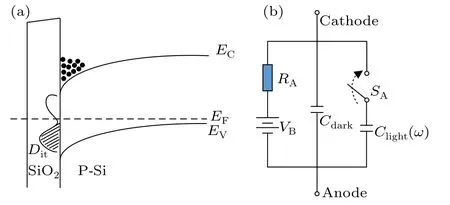
Fig.8.(a)Schematic of the SiO2/Si band with interface traps,(b)equivalent circuit model considering interface traps.
HereRAis the total resistance of the SPAD,VBis the breakdown voltage,and the switchSAsimulates the arrival of photons.In the dark state of the SPAD, the internal capacitance of the device is a capacitorCdarkthat does not change with frequency;when the device is in a light environment,the switchSAis closed, and an additional frequency-dependent capacitorClight(ω) is added to the equivalent circuit.When the energy level of the surface trap is displaced relative to the Fermi levelEF, the electron filling state in the trap changes,resulting in a change in charge.The intuitive effect of this change is a change in capacitance.When a reverse bias is applied to the SPAD in Fig.1,the energy band at the P+surface of the central photosensitive region is bent downward,and the energy level of the interface state moves downward relative toEF.When the acceptor state close to the conduction band moves toEF, due to the electrons occupying the acceptor interface state and the electrons accumulating at the surface of Si–SiO2,forming an accumulation phenomenon,there are additional negative charges in the interface state.
It can be seen that the change in the applied bias voltage causes a charge change in the interface state; that is, the charge–discharge effect occurs in the interface state.The interface defect state can be characterized in theC–Vcurve when the charge of the interface defect is exchanged with the photosensitive region P+, that is, the interface defect captures and emits electrons.Under no-light conditions, the interface defect states below the intermediate energy level of the forbidden band do not have the energy provided by photons and cannot capture and emit electrons normally.When the device absorbs the energy of the photon,the photo-generated carriers are exchanged with the interface defect state,which changes the capture rate of the trap,that is,reduces the lifetime of the trap.In other words,the energy brought by the light affects the emission and capture rates of electrons in the defect, resulting in a shortened trap lifetime.In addition, when the frequency of the small signal applied by the SPAD is high, the filling and release rates of trap states cannot keep up with the AC signal,which leads to a significant decrease in the photocapacitance of the device at high frequencies, and the photocapacitance exhibits frequency dependence.
4.Conclusion
The photocapacitance effect of SPADs is experimentally studied.First, to distinguish the general capacitance of the PN junction, SPAD capacitance is divided into dark capacitance and photocapacitance.The photon energy excites the device to generate photogenerated electron–hole pairs, which increases the internal carrier concentration, thereby increasing the capacitance.Second, it is noted that the photocapacitance has a frequency scattering effect, and the capacitance decreases significantly with increasing frequency.This is due to the existence of interface traps in planar silicon devices,and the photon energy affects the trapping rate of interface traps in SPAD devices,resulting in changes in trap lifetime.
Acknowledgments
Project supported by the National Natural Science Foundation of China (Grant Nos.62174052 and 61827812), Hunan Science and Technology Department Huxiang High-level Talent Gathering Project (Grant No.2019RS1037), Innovation Project of Science and Technology Department of Hunan Province (Grant No.2020GK2018), and Postgraduate Scientific Research Innovation Project of Hunan Province (Grant No.QL20210131).
- Chinese Physics B的其它文章
- Interaction solutions and localized waves to the(2+1)-dimensional Hirota–Satsuma–Ito equation with variable coefficient
- Soliton propagation for a coupled Schr¨odinger equation describing Rossby waves
- Angle robust transmitted plasmonic colors with different surroundings utilizing localized surface plasmon resonance
- Rapid stabilization of stochastic quantum systems in a unified framework
- An improved ISR-WV rumor propagation model based on multichannels with time delay and pulse vaccination
- Quantum homomorphic broadcast multi-signature based on homomorphic aggregation

