
SoftSSD:enabling rapid flash firmware prototyping for solid-state drives*&
2023-06-02 12:30:50JinXUERenhaiCHENTianyuWANGZiliSHAO
Jin XUE ,Renhai CHEN ,Tianyu WANG ,Zili SHAO
1Department of Computer Science and Engineering, The Chinese University of Hong Kong, Hong Kong 999077, China
2College of Intelligence and Computing, Tianjin University, Tianjin 300354, China
Abstract: Recently,solid-state drives (SSDs) have been used in a wide range of emerging data processing systems.Essentially,an SSD is a complex embedded system that involves both hardware and software design.For the latter,firmware modules such as the flash translation layer (FTL) orchestrate internal operations and flash management,and are crucial to the overall input/output performance of an SSD.Despite the rapid development of new SSD features in the market,the research of flash firmware has been mostly based on simulations due to the lack of a realistic and extensible SSD development platform.In this paper,we propose SoftSSD,a software-oriented SSD development platform for rapid flash firmware prototyping.The core of SoftSSD is a novel framework with an event-driven programming model.With the programming model,new FTL algorithms can be implemented and integrated into a full-featured flash firmware in a straightforward way.The resulting flash firmware can be deployed and evaluated on a hardware development board,which can be connected to a host system via peripheral component interconnect express and serve as a normal non-volatile memory express SSD.Different from existing hardware-oriented development platforms,SoftSSD implements the majority of SSD components(e.g.,host interface controller) in software,so that data flows and internal states that were once confined in the hardware can now be examined with a software debugger,providing the observability and extensibility that are critical to the rapid prototyping and research of flash firmware.We describe the programming model and hardware design of SoftSSD.We also perform experiments with real application workloads on a prototype board to demonstrate the performance and usefulness of SoftSSD,and release the open-source code of SoftSSD for public access.
Key words: Solid-state drives;Storage system;Software hardware co-design
1 Introduction
Recently,solid-state drives (SSDs) have been used in a wide range of emerging data processing systems(Lu LY et al.,2016;Lee et al.,2019).Compared to traditional magnetic disks,SSDs deliver higher input/output (I/O) throughput as well as lower latency,which makes them one of the best choices as the underlying storage for large-scale data processing systems demanding high I/O performance.The design of modern SSDs has gone through intensive optimizations to reduce request latency and improve throughput.Meanwhile,novel storage interface protocols,such as non-volatile memory express(NVMe),have been proposed to reduce communication overhead between the host and the device to harvest high I/O performance enabled by modern SSDs.Under the hood,SSDs persist data on NAND flash memory,which retains data after power loss(Boukhobza et al.,2017).The flash memory chips typically form an array with multiple channels so that user requests can be distributed among them to better use the I/O parallelism.
Although NAND flash memory is the core component of SSDs,it does not work off-the-shelf.A smart storage controller must be used to orchestrate the internal operations of SSDs and data flows between the host interface and the flash memory.By nature,the storage controller is a complex embedded system that involves both hardware and software design.The former includes physical interfaces to buses through which the storage controller is connected to the host and the underlying flash memory array.For the latter,firmware modules such as the flash translation layer (FTL) (Gupta et al.,2009;Ma et al.,2020)are implemented to handle internal operations and flash management of SSDs.In summary,the main task of a storage controller is to accept requests from the host interface,perform necessary transformations on them,and finally dispatch them through multiple channels to the underlying flash memory array.
Storage controllers are responsible for various operations on the critical path of request processing.Thus,the performance delivered by an SSD depends heavily on the storage controller.To handle a tremendous number of concurrent I/O requests arriving from multiple submission queues(SQs)provided by the flexible host interface protocol,the storage controller,especially the flash firmware running on top of it,needs to perform internal SSD operations such as address translation and cache lookup with high efficiency.On the other hand,the architecture of modern SSDs has been designed in a hierarchical manner,so that flash transactions can be distributed across multiple channels and executed in parallel to obtain the maximal throughput (Gao et al.,2014).Thus,the storage controller needs to handle the queuing and scheduling of flash transactions to fully use the massive internal I/O parallelism.These internal tasks can incur high computational load when there are a large number of concurrent user requests and the flash firmware can soon become a bottleneck if the FTL algorithms are not well designed.Furthermore,manufacturers begin to employ highperformance multi-core microprocessors on SSDs to adapt to the massive I/O parallelism of the underlying flash storage.With a multi-core processor,the flash firmware can start multiple worker threads to process the computational work in parallel to improve throughput and hide request latency (Zhang et al.,2020).This opens new opportunities in flash firmware research,in which an extensible SSD development board is required for rapid prototyping and evaluation.
Despite the rapid development of new features of SSDs in the market,the research of flash firmware has been mostly based on simulations due to the lack of a realistic and extensible SSD development platform.Existing SSD simulators (Kim et al.,2009;Hu et al.,2011;Yoo et al.,2013;Jung et al.,2016,2018;He et al.,2017;Li HC et al.,2018;Tavakkol et al.,2018) typically model only some parts that are considered to have the most significant impact on the end-to-end latency,e.g.,data transfer and flash command execution.The simplified latency model used by these simulators may not accurately capture the performance characteristics of real SSDs.For instance,many simulators model a single-queue host interface that reflects older protocols such as serial AT attachment(SATA),instead of newer storage protocols such as NVMe which provide multi-queue support and higher performance.Meanwhile,due to the physical characteristics of NAND flash,errors may occur during the read and the program processes,and data may be lost as a result of NAND flash wear-out after many program/erase cycles.Such physical characteristics have a negative effect on the SSD performance(Shi et al.,2016),but are not modeled by existing SSD simulators.As such,these simulation tools may not provide SSD performance results that match those of the real hardware.
Conventionally,many components of a storage controller,such as the host interface controller,the flash transaction scheduler,and the error correction code (ECC) engine,are implemented in hardware on a field-programmable gate array (FPGA) or an application-specific integrated circuit (ASIC).Although such a hardware implementation can generally achieve higher performance compared to its software counterpart,it causes several difficulties for investigating and prototyping new flash firmware.Due to the complexity of modern storage protocols,implementing a host interface controller in pure hardware requires non-trivial effort.Also,new extensions and new transports,such as the NVMe keyvalue(KV)command set and the remote direct memory access (RDMA),are continuously added to existing storage protocols to adapt to emerging data models used in current data processing systems.If the host interface controller is implemented in hardware,it can be time-consuming to extend the hardware design to support the new extensions,making prototyping flash firmware for these new interfaces difficult.
To bridge the gap between pure software simulation-based platforms and hardware-oriented platforms,we propose SoftSSD,a novel softwareoriented and flexible SSD development platform for rapid flash firmware prototyping,as shown in Fig.1b.The core of SoftSSD is a development board that can be plugged into a host machine and serve as a normal NVMe SSD.Different from existing hardwareoriented approaches,we implement only a small number of necessary components in the storage controller in hardware on an FPGA.These components include the physical layer interfaces to the host bus,e.g.,the peripheral component interconnect express(PCIe) link,and the NAND flash chips.Such interfaces are defined by specifications and thus not subject to frequent changes.Furthermore,these hardware components are required only to handle simple tasks such as receiving raw transaction layer packets (TLPs) from the PCIe link,so that they can be extended to support newer revisions of the interfaces.Other components of SoftSSD,including the NVMe interface and the flash transaction scheduler,are developed in pure software as parts of the flash firmware modules and run on an ARM-based embedded processor.These components as well as the flash firmware can be reconfigured and reprogrammed for research purpose.With SoftSSD,data flows and internal states that were once confined in the hardware design are now processed by the software and can be examined with a debugger,which provides observability and visibility in rapid prototyping and flash firmware research.
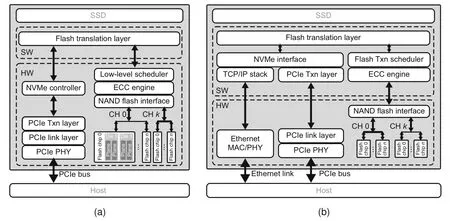
Fig.1 Comparison of existing hardware-oriented platforms (a) and SoftSSD (b)
However,implementing SSD components in software brings new challenges.First,compared to specialized hardware implementations,software implementations provide more flexibility at the cost of lower performance,which poses a great challenge in SoftSSD.Second,as SSD components are now an integrated part of the flash firmware,a new programming model is required to hide the details of interacting with the hardware and enable implementing and assembling these modules,including the FTL,into flash firmware in a straightforward way.To this end,we propose a novel framework with an event-driven threaded programming model,on which the flash firmware is built for SSD firmware.Under the framework,user requests are handled as small tasks that can be assigned to multiple threads and scheduled to maximize central processing unit (CPU) utilization and thus enhance the SoftSSD performance.Furthermore,the flash firmware built with the proposed framework can be deployed on a multi-core heterogeneous microprocessor to process I/O requests in parallel.
We implement both the programming model and the hardware components of SoftSSD and carry out performance evaluation.We connect SoftSSD as a standard NVMe SSD to a real host system and conduct experiments with application workloads to demonstrate the performance of SoftSSD.We also compare our software-implemented NVMe interface with an FPGA-based NVMe controller.Experimental results show that SoftSSD can achieve good performance for real I/O workloads while providing observability and extensibility for rapid flash firmware prototyping.SoftSSD has been released as open source at https://github.com/Jimx-/softssd.
This work is a revised version based on a preliminary version of our work published in Proceedings of the 2022 IEEE 40thInternational Conference on Computer Design (Xue et al.,2022).The new contributions of this paper are summarized as follows:
1.We add a new section to present more background information about existing SSD development platforms and open-channel SSDs (Section 2.2).We also add Table 1 to summarize the differences between our proposed platform and existing SSD platforms.
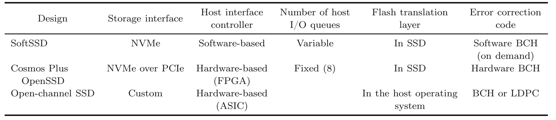
Table 1 Summary of different SSD development platform designs
2.We analyze the overhead of the softwarebased PCIe TLP processing and its impact on direct memory access (DMA) request performance (Section 3.1).We add a new optimization that offloads the packet processing to FPGA fabric to improve the DMA performance.
3.We add a new optimization on the ECC engine to separate the detection and correction of errors in data blocks and bypass the expensive softwarebased correction for clean blocks(Section 3.2).
4.We analyze the performance overhead of the software-based host interface controller by implementing a hardware NVMe-over-PCIe controller in the FPGA and comparing its performance with that of SoftSSD (Section 6.5).
2 Background
2.1 NVMe SSD devices
Fig.1 illustrates the overall architecture of a modern NVMe SSD.As shown in Fig.1,the SSD is connected to the host via a physical bus,most commonly PCIe.The physical bus interface allows the SSD and the host to exchange requests and data.Based on that,an NVMe controller manages the internal states of the storage protocol and parses incoming requests.The requests are processed by an FTL executing on a microprocessor.The FTL performs the necessary transform on the requests,converting the requests into flash commands (e.g.,read and program) executed by the NAND flash memory.The processor is connected to the flash memory components through an NAND flash interface which contains multiple bus channels.Each channel is connected to one or more NAND flash memory chips.
To maximize the I/O parallelism,a flash chip is further organized in a hierarchical structure,as shown in Fig.1.Specifically,a flash chip is divided into multiple dies or logical units(LUNs),where each die has its own command and status register.This allows dies to execute different commands independently in parallel.Each die is further divided into multiple planes,where each plane has separate cache and data registers.Through multi-plane commands,multiple planes in the same die can execute the same operation to the same offset within the plane concurrently.Finally,a plane is divided into multiple blocks and flash pages.
Due to the physical limitations of NAND flash memory,errors may occur during the read and the program processes.The cells that store data bits may wear out as a result of continuous program and erase operations so that some memory locations may no longer be programmed or erased properly.To ensure data integrity,it is crucial to equip the SSD with a mechanism that is capable of detecting and correcting a certain number of bit errors(Wang et al.,2017).The ECC engine encodes data programmed on the NAND flash memory in a way such that errors can be identified and corrected by the decoder when the data are read(Li S and Zhang,2010;Ho et al.,2013).For write operations,the ECC engine generates a code word for the flash page data,which is stored in the out-of-band(OOB)area of the data page.When reading data from the NAND flash memory,both the flash page data and the code word are retrieved.By comparing the code word re-computed from the read data and the stored code word,error bits can be identified.If a flash page contains more error bits that can be corrected by the ECC engine,the block of this flash page is marked as a bad block by the flash firmware and will not be used.
In an NAND flash memory chip,a flash page(typically 4–16 KB)is the basic data unit for a read or write operation.In addition to the user data area,each flash page has a small OOB area that can be used by the flash firmware to store internal metadata such as the ECC.The flash pages are grouped into blocks,which are the granularity for an erase operation.Once data are written to a flash page,the flash page cannot be updated until it is later reclaimed and erased.Thus,SSDs generally do not support in-place updates for flash pages.Instead,pages are updated in an out-of-place manner.When a logical page is updated,the flash firmware allocates a newly erased physical page.After that,existing data for the logical page are read from the old physical location,merged with the update,and written to the new location.The logical-to-physical address mapping is updated so that subsequent requests to the logical page will be redirected to the new physical location.In this way,the old physical page (and all pages in the same flash block) does not need to be erased for the update,and thus the high erase latency is avoided for a write operation.However,because the logical page is now mapped to a new physical location,the old physical page must be marked invalid so that background garbage collection(GC)can be run later to reclaim the invalid flash pages (Yang et al.,2014).These internal details of NAND flash memory are handled by the FTL to expose a symmetric block access interface.
2.2 SSD development platforms
In recent years,open-source hardware SSD platforms such as Jasmine OpenSSD and Cosmos Plus OpenSSD (Kwak et al.,2020) were introduced to provide a realistic platform for the research of storage controllers.Both implementations provide development boards that can be connected to the host through a specific host interface (e.g.,SATA and NVMe) and used as a normal SSD.Based on that,some parts of the system can be reconfigured or re-implemented for research purpose.However,Jasmine OpenSSDs are based on a commercial ARM-based SATA controller system-on-a-chip(SoC).Thus,with Jasmine OpenSSDs,only the flash firmware can be modified to implement new flash management algorithms,but the underlying hardware components cannot be extended to support newer storage protocols such as NVMe.Cosmos Plus OpenSSD,on the contrary,implements the hardware components of the storage controller,e.g.,the host interface controller,the flash controller,and the ECC engine,on an FPGA,as shown in Fig.1a.Although this design makes it possible to modify the host interface and the flash controller to support newer protocols,it still requires significant efforts to develop and maintain these components on an FPGA.Also,compared to a software implementation,hardware implementations based on FPGA lack observability and extensibility that are critical to the prototyping and debugging of newer storage techniques.For example,the Cosmos Plus OpenSSD hardware NVMe controller supports only up to eight NVMe I/O queues,which is hard-coded in the design.To support more queues,the hardware design must be modified to add state storage and arbitration logic for the extra queues,which is error-prone.On the contrary,a software NVMe controller allows the host to transparently create a large number of I/O queues as long as they do not exceed device DRAM capacity.In this way,a software-based development platform can be extended to support workloads with a higher degree of queue-level parallelism without modifying the hardware components.For observability,with a hardware-based development platform,the hardware design needs to be modified to capture relevant internal signals for examination,whereas for a software-based platform,all internal states of the software components can be exposed to developers with a software debugger.
Due to the difficulty in implementing all SSD functionalities on the development platform,some works proposed open-channel SSDs (Lu YY et al.,2013;Bjørling et al.,2017)to reduce the device-side complexity.Different from traditional SSDs,openchannel SSDs do not have an FTL implemented on the device.Instead,the device exposes the internal organization and characteristics of flash memory and leaves the SSD management tasks to the host.In this way,FTL components such as the mapping table and GC can be implemented in the host operating system.Although open-channel SSDs provide a flexible approach for evaluating different FTL algorithms,they may require a significant amount of host memory and CPU cycles for SSD management.Furthermore,by treating the SSD as a raw flash memory device without minimal computation capabilities,applications that can be built based on such platforms are restricted.For example,in-storage computing (ISC) allows the host to offload computation tasks to the storage device for execution to reduce host-device data movement cost.However,such ISC applications are not supported by openchannel SSDs because they lack both the processing elements required to execute in-storage computation tasks and FTL metadata for in-situ flash data access.Table 1 summarizes the differences among these SSD platforms.
SoftSSD is a development platform that involves both hardware and software design.In this section,we focus on the hardware design of SoftSSD,which is a minimal set of functionalities that manage the interactions with the host and the underlying NAND flash array.The overall architecture of the SoftSSD hardware components is shown in Fig.2.

Fig.2 Overall architecture of the SoftSSD hardware components
3 Hardware design
3.1 PCIe interface
The software-oriented approach of SoftSSD enables building a storage protocol controller on top of different transports.In this work,we focus on the NVMe protocol over a PCIe transport layer.A PCIe interconnect can be regarded as a packet-based network.Similar to TCP/IP networks,PCIe adopts a layered model that consists of a physical layer,a data link layer,and a transaction layer.The data link layer manages the link state and ensures the data integrity of PCIe packets as they are delivered across the PCIe link.The PCIe transaction layer delivers TLPs between two PCIe endpoints across the PCIe links.The root complex and PCIe switches route and forward TLPs based on the destination addresses provided in the packets.Other functionalities of PCIe are built on top of this packet-based communication.For example,to perform DMA to the host memory,a PCIe device sends a memory read(MRd)or memory write(MWr)transaction packet with the data payload to the root complex.The root complex has access to the host memory and it completes the transaction based on the TLP and optionally sends back a completion packet to the requesting device for non-posted requests (e.g.,MRd).Message-signaled interrupts (MSIs) are sent from a PCIe device to the host by writing pre-configured data to a memory address specified by the interrupt controller.
In SoftSSD,we build only the physical and the data link layers in hardware on the FPGA.The two layers receive/transmit raw TLPs from/to the PCIe link.TLPs received from the link or to be transmitted are divided into two streams based on whether the device is the requester or the completer of the transaction.Two DMA interfaces move the raw TLPs between the PCIe controller and the device DRAM.After the raw TLPs arrive at the device DRAM,they are parsed and processed by the software PCIe transaction layer.The completer interface handles MRd or MWr requests from the host to the memory-mapped I/O regions exposed by Soft-SSD through the base address registers(BARs).For MWr requests,the write data are attached as payload in the TLPs and the device does not need to send back completion packets to the host.MRd requests contain a unique tag but do not have any data payload.Upon processing an MRd TLP,the software transaction layer sends a completion TLPcontaining the read data with the same tag as the request packet.The requester interface is used by the flash firmware to initiate DMA requests to the host memory.To send a DMA request,the flash firmware prepares a TLP in the device DRAM and configures the requester DMA controller to move the packet to the PCIe controller for transmission to the PCIe link.For DMA read requests,the host sends back response data with a completion TLP,which is moved to the device DRAM and processed by the software transaction layer.
The performance of DMA requests to the host memory depends mainly on the requester DMA interface.For a PCIe device,the maximum size of the payload in a TLP may be different from the maximum size allowed for an MRd request.For this reason,an MRd request may be completed with one or multiple completion TLPs.With a full software transaction layer,all completion TLPs for a read request need to be copied to the device DRAM and processed by the software.The software transaction layer may further copy the data payload of the completion TLPs and re-assemble the response data in a data buffer,incurring high data movement and software packet processing overhead and causing a bottleneck for DMA request performance.
To improve host DMA request performance,we offload the processing of requester completion TLPs from the software transaction layer to the requester DMA controller.As shown in Fig.3,the requester DMA controller internally records the data buffer addresses of up to 64 outstanding host memory DMA read requests in the buffer descriptor table.The buffer descriptor table also stores the current offset for each data buffer,which is the number of bytes already received for the read request.When initiating a new DMA read request to the host memory,the flash firmware allocates a unique tag for it and registers the buffer base address in the buffer descriptor table.Upon receiving new completion TLPs with response data,the requester DMA controller extracts the tag from the TLP and obtains the buffer address from the table.The data mover copies the data payload to the corresponding position in the data buffer and updates the offset.After the last completion for a DMA read request is received,the requester DMA controller sets the corresponding bit in the completion bitmap and notifies the flash firmware.With the offloading,the number of TLPs processed by the software transaction layer is reduced and the software does not need to repeatedly copy the data payload to re-assemble the response data,thus improving the host DMA request performance.
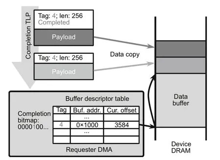
Fig.3 Completion TLP processing offloading to the requester DMA controller
Overall,the following listing shows the application programming interface (API) provided by the PCIe controller and the software PCIe transaction layer.The flash firmware defines the callback functions to handle memory read/write requests to the memory-mapped BAR regions.pcie_send_completion sends response data to complete a memory read request by the host.The flash firmware can use pcie_dma_read/write to transfer data between the host memory and the device DRAM.Finally,pcie_send_msi can be used to send an MSI/MSI-X (short for message signaled interrupt/extended message signaled interrupt) to the host with the provided interrupt vector.
void pcie_mem_read_callback(int bar_nr,unsigned long addr,u16 requester_id,u8 tag,size_t len);
void pcie_mem_write_callback(int bar_nr,unsigned long addr,const u8* buf,size_t len);
int pcie_send_completion(unsigned long addr,u16 requester_id,u8 tag,const u8*buffer,size_t count);
int pcie_dma_read(unsigned long host_addr,u8* buffer,size_t count);
int pcie_dma_write(unsigned long host_addr,const u8* buffer,size_t count);
void pcie_send_msi(u16 vector).
3.2 Error correction bypass
In this work,we use the Bose–Chaudhuri–Hocquenghem (BCH) code as the encoding scheme for ECC.With the BCH code,user data are divided into multiple blocks of fixed size and a block of code bits is calculated and appended to the data block.The code bits are stored with the user data in a flash page.When the data are read from the NAND flash memory,a decoder processes the data and code bits to detect and correct errors in the data.The decoding of the BCH code involves several phases.First,the syndromes are calculated from the read data and code bits.Based on the syndromes,we can detect whether there are errors in the data.If the syndromes are all zero,the read data do not contain any error bit and the decoding is finished.Otherwise,error locations are computed from the syndromes and the corresponding bits are flipped to correct the errors.Although the error correction is complex and requires more computational power,the error detection phase can be done in a streaming manner with fewer hardware resources.For this reason,we implement the complex error correction logic in software but offload the encoding and the error detection logic to the hardware.
As shown in Fig.4,instead of storing ECC code bits in the OOB area of a flash page,we store the data blocks and code bits in an interleaving manner.This data layout allows us to perform data encoding and decoding in a streaming manner during data transfer without buffering any data.When writing data to a flash page,the DMA controller reads the user data from the device DRAM,separates them into data blocks,and streams them into the BCH encoder.The BCH encoder appends BCH code bits after each data blocks,which will be written to the flash page by the NAND flash controller.When reading flash pages from the NAND flash memory,the data are first segmented into frames that contain data blocks and the stored code bits.The frames are streamed into the BCH detector,which detects if there are errors in the data blocks without attempting to correct them.The error information is recorded in an error bitmap which can be accessed by the software ECC engine later.After the BCH error detector processes the data,the DMA controller uses scatter-gather DMA requests to write data blocks and code bits to the device DRAM.During this process,data blocks and ECC code bits are separated,and the original user data layout is restored.The software error correction engine then checks the error bitmap to determine which blocks in the user data contain error bits and corrects error bits in these blocks.
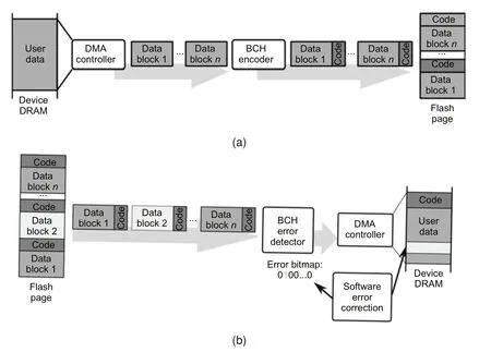
Fig.4 Data flow for writing to (a) and reading from (b) flash pages
Compared to error correction,the encoding and error detection logic consumes fewer hardware resources,which allows us to build one ECC encoder and one ECC error detector per each flash channel.This enables us to perform data encoding and error detection during the data transfer without incurring extra overhead.Once the ECC detector checks that a data block is free of errors,it can be forwarded to the flash firmware without further processing.Only blocks that contain error bits need to be sent to the software ECC engine to correct errors.With the error correction bypass,we can skip the expensive software error correction logic for most data blocks,which is more efficient than existing methods that share the hardware ECC engine among multiple channels in a time-division manner and significantly reduces request latencies.Although we reuse the same encoding scheme for both hardware error detection and software error detection in this work,it is also possible to implement error detection with a different encoding scheme,such as the cyclic redundancy check (CRC).In this way,we can implement the entire ECC engine in pure software for better flexibility.
Overall,the hardware components in SoftSSD enable the flash firmware to interact with the host and NAND flash memory via different interfaces.On one hand,the PCIe controller and the software PCIe transaction layer allow the flash firmware to initiate and process memory transactions over a PCIe link.On the other hand,the flash channel controllers retrieve data from the NAND flash memory and check data integrity for the flash firmware.
4 Software design
Based on the minimal set of functionalities implemented by the hardware design,we can build the flash firmware to serve user requests.In this section,we discuss the programming model and the implementation of the software components in SoftSSD.
4.1 Programming model
FTL processing of a user request involves multiple blocking operations and may be suspended before such operations complete.For example,before issuing a flash command to write data to the NAND flash memory,the flash firmware needs to wait for the PCIe controller to transfer the write data from the host memory into internal buffers in the device DRAM.To exploit the data access parallelism,the flash firmware should continue to process new requests when the current request is blocked on host DMA/flash access operations instead of waiting for the operation to complete.For this reason,the flash firmware needs to efficiently switch between requests once a request is blocked so that multiple requests can be processed in a concurrent manner.Existing methods tackle this problem by separating the request processing into several stages.A user request of an arbitrary size is divided into slice commands that request fixed-sized data.Each stage processes one slice command at a time and when a slice command is blocked,the stage puts the command in an internal output queue for the next stage to retrieve.After the blocking operation completes,the slice command is resumed by the next stage.As such,user requests are processed in a pipelined manner to maximize the throughput.However,existing FTL algorithms still need to be re-designed and manually divided into multiple stages based on the possible suspension points to be used on the existing SSD platform.Furthermore,there can be dependencies between different stages.For example,during the address translation stage,requests may be issued to the flash transaction stage to read in pages that contain translation information.Such dependencies make it more difficult to implement the FTL algorithm as multiple stages.
In SoftSSD,instead of dividing the flash firmware into stages,we map user requests to threads.Each request accepted through the NVMe interface is assigned to a thread,which runs the request until its completion.Once a request is blocked on data transfer or flash operations,its thread is switched out so that other requests can be processed in an interleaving way.Fig.5 shows an example of concurrent request processing with two threads.During the processing of a user request,the execution may be blocked due to various operations.For example,during the address translation,the FTL may need to issue flash read commands to load missing mapping table pages from the flash memory(mapping table read).It can also be blocked on DMA transfers between the host memory,the device DRAM,and NAND flash memory (host DMA and flash DMA).Whenever a thread is blocked on a specific operation,it puts itself in a wait queue and suspends itself.The scheduler then picks the other thread with pending user requests to continue execution.Later,when the operation completes,the scheduler is notified and it checks the wait queue to resume the suspended threads.With the framework,we can overlap computation tasks with blocking I/O operations so that multiple NVM requests can be processed concurrently to fully use data access parallelism and maximize the throughput.Also,the entire request processing is implemented as a monolithic threaded function in a straightforward way without dividing FTL algorithms into multiple stages connected through message queues.
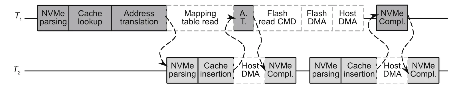
Fig.5 An example of request processing under the proposed programming model with two threads
In this work,we use a coroutine-based asynchronous framework to implement the proposed programming model.Coroutines(Conway,1963;Moura and Ierusalimschy,2009;Belson et al.,2019)are similar to normal functions,but their execution can be suspended and resumed at manually defined suspension points.Local variables used by a coroutine are preserved across suspensions until the coroutine is destroyed.Specifically,we implement one variant called stackful coroutines,in which each coroutine has its own separate runtime stack instead of sharing the stack of the underlying thread.With stackful coroutines,local states and the call stack of a coroutine are preserved on the private stack.Nested coroutine calls are simply function calls that do not incur extra overhead.Context switches between coroutines have the same effect as that of saving and restoring a small number of callee-saved registers on the coroutine stack,including the stack pointer and the program counter.Stackful coroutines can be implemented as a general-purpose library without special syntax (e.g.,async/await) provided by the language compilers,and FTL algorithms can be integrated into the asynchronous framework with minor modifications.
4.2 Heterogeneous multi-core architecture
To handle a tremendous number of concurrent I/O requests arriving over multiple queues,manufacturers begin to employ high-performance multi-core microprocessors with more computational power on SSDs.In SoftSSD,we run the flash firmware on an ARM-based heterogeneous multi-core microprocessor with one 64-bit Cortex-A53 core and two 32-bit Cortex-R5 cores,as shown in Fig.6.To better use the parallel processing enabled by the multi-core processor,we adopt a layered design for the flash firmware and divide it into three modules that can independently run on different CPU cores.The FTL module implements the software NVMe interface,which communicates with the host OS driver through the PCIe controller.It also handles most computational tasks(i.e.,cache lookup and address mapping)for a user request.Thus,we run the FTL module on the Cortex-A53 core with the highest computational power.The flash interface layer(FIL)module manages the low-level flash transactions issued by the FTL module and dispatches them to the NAND flash memory through the flash channel controllers.It also continuously sends commands to the NAND flash memory to poll the NAND device status.Finally,the ECC engine module implements the software error correction logic to ensure data integrity.

Fig.6 Multi-core heterogeneous architecture of SoftSSD
The FTL module communicates with the FIL and the ECC engine modules with two ring queue pairs located in a shared memory region.Each queue pair has an available ring and a used ring.When the FTL module needs to send a request to the other two modules,it enqueues a command in the corresponding available ring.The FIL and the ECC engine modules continuously poll the available ring for new commands.For the FIL module,each command represents a read or write flash transaction that needs to be executed on the target flash chip.For the ECC engine module,each command contains the data block and the corresponding stored code bits that need to be corrected.After a command is processed,the two modules enqueue a completion entry in the used ring and send an inter-processor interrupt (IPI) to the FTL module to notify it of the command completion.
4.3 NVMe interface
In SoftSSD,we implement the NVMe protocol completely in software for better observability and extensibility.With NVMe,the host OS creates multiple queue pairs in the host memory for submitting commands and receiving completion.Internally,the flash firmware starts multiple coroutine threads to handle the requests from one queue pair.Each NVMe worker thread is bound to an NVMe SQ.After a worker thread is started,it continuously polls the SQ for new commands.If the SQ is empty (i.e.,the head pointer and the tail pointer meet),then the worker thread suspends itself and waits until new commands arrive.Otherwise,it fetches the command at the head pointer with a host DMA request through the PCIe controller and updates the head pointer.The command is handled as either an admin command or an I/O command based on the SQ,from which it is received and the command result will be posted to the corresponding completion queue(CQ).Finally,the worker thread sends an MSI to the host to notify it of the command completion.When the host writes to the SQ tail doorbells,a callback function will be invoked with the new tail pointer.If the new tail pointer is different from the current value,it updates the tail pointer and wakes up all worker threads assigned to the SQ to process the new commands.
4.4 Flash interface layer
The FIL manages the low-level flash transaction queues and the underlying NAND flash array.To avoid contention between FTL tasks and flash management tasks,we offload the FIL to a dedicated CPU core.The FTL core and the FIL core communicate via a pair of ring queues(the available ring and the used ring) located in a shared memory.The FTL divides user requests of arbitrary sizes into fixed-sized flash transactions and submits them to the available ring.Each flash transaction reads/writes data from/to a flash page identified by its physical address.The physical address is represented as a location vector(channel,way,die,plane,block,page) based on the flash array hierarchy.At runtime,the FIL first polls the available ring for incoming flash transactions.The flash transactions are organized into per-chip transaction queues based on the channel and the way number in their location vectors.Each flash transaction is executed in two phases: the command execution phase and the data transfer phase.Based on the flash transaction type,the command execution phase either reads data from the NAND flash cells into its internal data cache or programs the data in the cache to the flash cells.The data transfer phase transfers data between the device DRAM and the internal data cache.The two phases can be started only if the target die or the channel is idle.Thus,the FIL goes through the transaction queues of all chips that are connected through an idle channel or have at least one die that is not executing any flash command and dispatches the flash transactions to them if possible.The FIL also maintains the list of flash channels and dies with outstanding data transfers/flash commands.It polls the status of the flash channel controllers and the flash dies to check if the data transfers or the flash commands have completed.Once the two execution phases for a flash transaction complete,the flash transaction is added to the used ring and the FIL generates an IPI to notify the FTL core of the completion.
5 Implementation
We implement the prototype of SoftSSD on a hardware development board as shown in Fig.7.The core of the SoftSSD board includes a dualcore ARM Cortex-A53 application processing unit(APU),a dual-core ARM Cortex-R5 real-time processing unit (RPU),and programmable logics built into the FPGA.We use one APU core to run the worker coroutine threads of the FTL and two RPU cores to run the FIL and the ECC engine,separately.The SoftSSD board is designed as a PCIe expansion card that can be connected to the host system with PCIe Gen3×8 and serve as a normal NVMe SSD.The flash memory modules are mounted with eight test sockets.The NAND flash packages are connected to the FPGA with eight NV-DDR2 channels specified by the open NAND flash interface(ONFI).The two packages in the same row share two channels and the storage controller supports up to an 8-channel,4-way configuration.SoftSSD enables rapid flash firmware development by implementing a large number of SSD components in software.
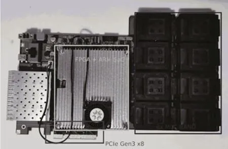
Fig.7 Hardware development board of SoftSSD prototype
Multiple FTL algorithms can be integrated with the coroutine-based asynchronous framework to provide full-featured flash firmware.In this work,we implement FTL based on the demand-based flash translation layer(DFTL) (Gupta et al.,2009).The FTL uses a page-level mapping table to directly translate a logical page address into a physical one.Mapping table entries are stored as translation pages on the NAND flash memory and partially cached in the device DRAM for faster accesses.The global translation directory maintained in the embedded multimedia card (eMMC) keeps track of the physical locations of the translation pages.
6 Evaluation
6.1 Experiment setup
All experiments are conducted on a host PC with a 6-core Intel®CoreTMi7-8700 CPU and 16-GB RAM.The host PC runs Linux kernel 5.16.The workloads used in the experiments are generated by FIO-3.28.The SoftSSD prototype board is connected to the host PC via PCIe and used as an NVMe block device driven by the OS driver.An additional development PC is used to collect software output and statistics with a debug console via the universal asynchronous receiver/transmitter(UART)serial port.The development PC also runs the development tools for programming the prototype board.
For the SoftSSD prototype board,we install eight Micron MT29F1T08 MLC NAND flash memory chips(128 GB each).We enable NV-DDR2 timing mode 7 with a maximum data rate of 400 MT/s per channel.The OS driver creates 12 NVMe I/O queues on the device (one per host CPU hardware thread) and the maximum queue depth is set to 1024.Table 2 summarizes the SoftSSD configuration and the flash microarchitecture that are used in the experiments.
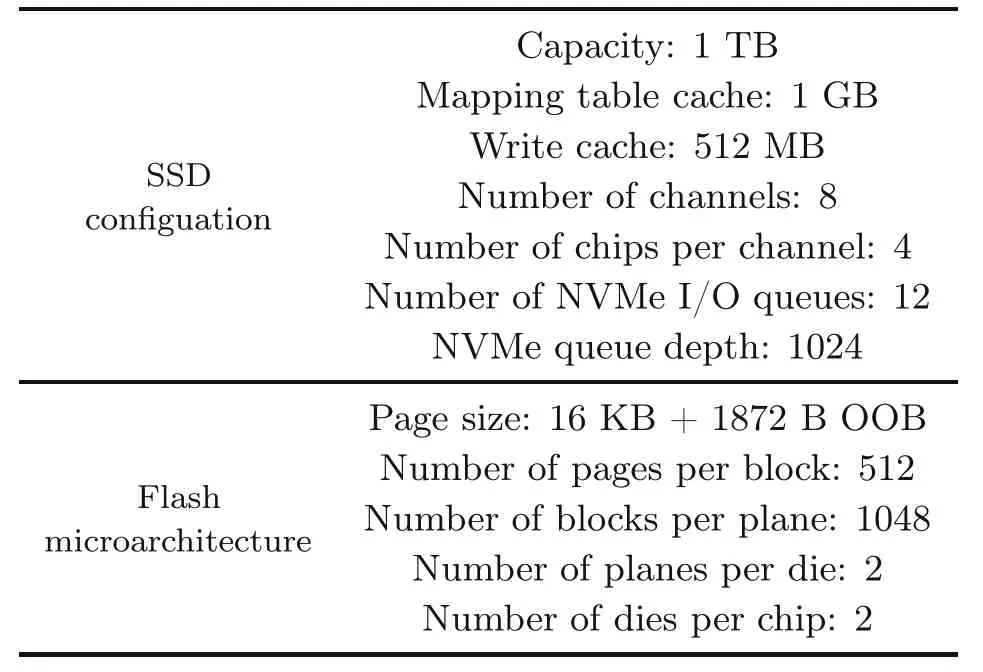
Table 2 SSD configurations used in the experiments
6.2 Sequential access
We first measure the sequential access performance of the SoftSSD prototype board.We use flexible I/O tester (FIO) to generate workloads that issue read or write requests to consecutive logical addresses.The queue depth is set to 1 and the number of outstanding requests to the SSD matches the number of threads.The request size is 1 MB for read requests and 16 KB for write requests.All experiments start with an empty mapping table and every accessed logical address is assigned a new physical address by the address mapping unit.For write requests,we issue enough requests to fill the write cache and cause the data cache to evict pages to NAND flash memory.
As shown in Fig.8,as the number of threads increases from 1 to 16,the throughput for both read and write requests increases.The throughput peaks at 32 threads,where all 32 flash chips (8-channel,4-way) are saturated with the outstanding flash commands.When the number of threads is small (e.g.,1–4),write requests have a lower throughput than read requests due to the longer flash command latency.As the number of threads increases,there are enough requests to saturate the bandwidth of the software host interface so that read and write requests achieve similar peak throughput.
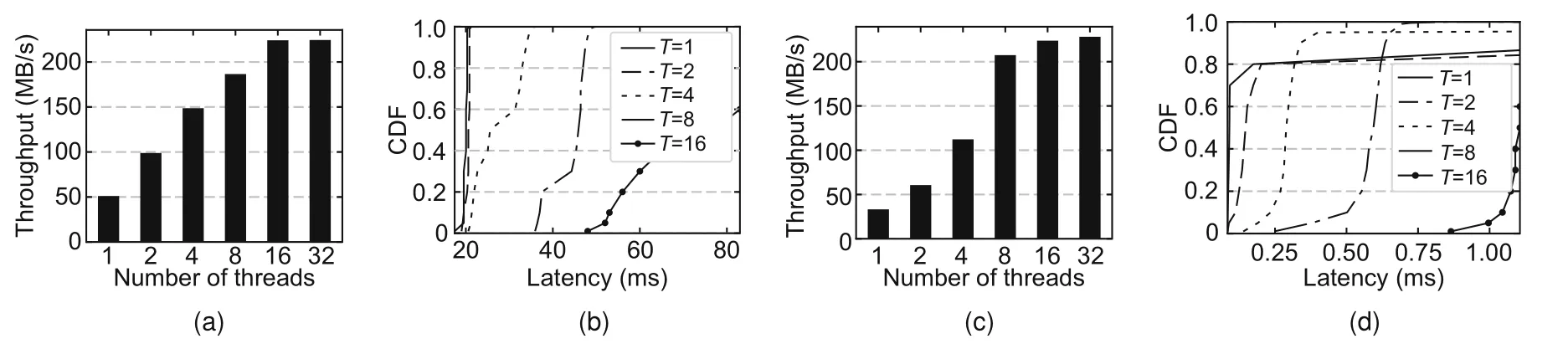
Fig.8 Sequential access performance of SoftSSD with different numbers of I/O threads: (a) read 1 MB throughput;(b) read 1 MB latency CDF;(c) write 16 KB throughput;(d) write 16 KB latency CDF (CDF:cumulative distribution function; T: number of threads)
Figs.8b and 8d also show the cumulative distribution functions (CDFs) of end-to-end read and write latencies,respectively.Compared to write latencies,read latencies have a more uniform distribution because data read from the NAND flash memory are not cached in the device DRAM and every read request incurs the same number of transactions to the NAND flash memory.For write requests,data can be buffered in the device DRAM before the data cache is full.After the data cache is filled,data must be evicted and written back to the NAND flash memory to make room for new data,and write requests may incur extra flash write transactions,causing the longer tail latency.
6.3 Random access
Fig.9 shows the average throughput and latency CDF of random accesses in SoftSSD.The workloads in the experiments issue read/write requests of 16 KB of data to random logical addresses.The queue depth is set to 1 and the number of outstanding requests to the SSD matches the number of threads.As shown in Fig.9,as the number of threads increases from 1 to 16,the input/output operations per second (IOPS) increase,and peak at 32 threads.Compared to sequential accesses,random read/write accesses achieve a lower maximum throughput due to worse locality.This has a negative impact on different components in the FTL.The mapping table needs to allocate and maintain more translation pages to store the physical addresses of the random logical addresses.Also,the data cache cannot use the temporal locality to coalesce multiple write requests with a cached page,incurring more flash write transactions.
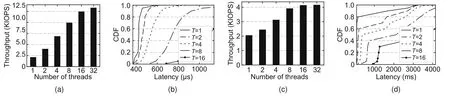
Fig.9 Random access performance (16 KB) of SoftSSD with different numbers of I/O threads: (a) read throughput;(b)read latency CDF;(c)write throughput;(d)write latency CDF(CDF:cumulative distribution function; T: number of threads)
6.4 Flash transaction latency
In SoftSSD,each flash transaction is executed in two phases.In the transfer phase,data are transferred between the device DRAM and the internal data cache in the NAND flash memory.In the command phase,the NAND flash memory executes a flash command to read/program data cache from/to NAND flash cells.With the software implementation,we can use the audit framework to collect performance statistics of different internal operations.Fig.10 shows the latencies of individual execution phases of flash transactions by running 16 KB aligned random read/write requests.
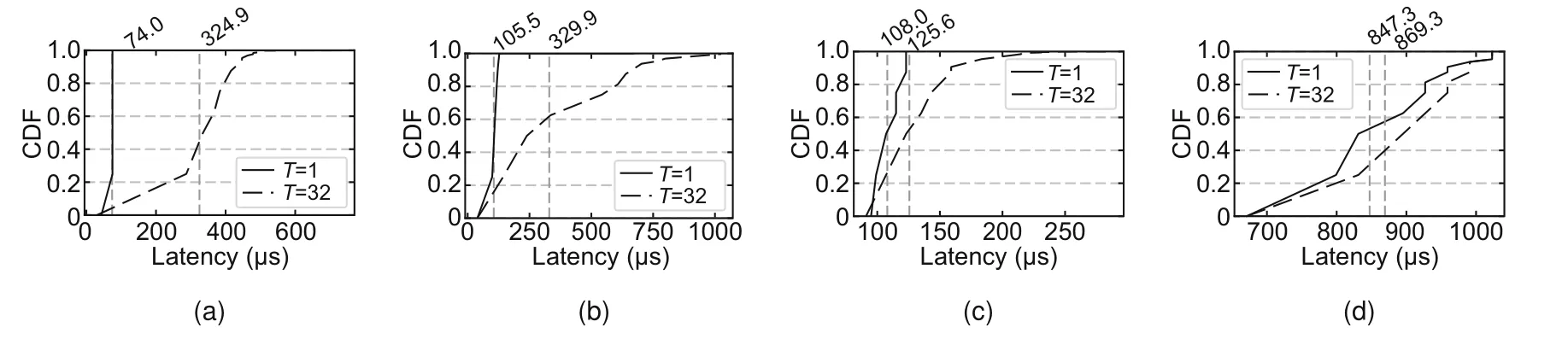
Fig.10 Latency CDFs of individual phases of flash transactions: (a) read transfer;(b) read command;(c)write transfer;(d) write command (CDF: cumulative distribution function; T: number of threads)
As shown in Fig.10,when a single thread is used,SoftSSD achieves deterministic latencies for the transfer phase (74.0 μs read,108.0 μs write)and the read command phase (~105 μs).When 32 threads are used,the flash transaction latencies increase due to the scheduling overhead and contention at the bus interconnects which connect the flash channel controllers to the device DRAM.Specifically,when there is a large number of outstanding flash transactions,the FIL core needs to continuously monitor the completion status of up to 64 flash dies,resulting in longer command latencies.Also,when used in multi-level cell(MLC)mode,each flash cell is shared by a lower LSB (short for least significant bit) page and an upper MSB (short for most significant bit)page with different read/program latencies,which is reflected by the steps of the write command latencies.
6.5 Software overhead
Different from existing methods,SoftSSD implements the majority of components in software for better extensibility.However,this could also incur overhead and degrade the overall performance compared to a specialized hardware implementation.For example,the host interface controller needs to transfer all PCIe TLPs to the device DRAM and process them in software.It also needs to maintain the internal states and provide a software simulation of the NVMe protocol.To evaluate the overhead of the software layer,we implement a hardware NVMe-over-PCIe controller in the FPGA and compare its performance with that of SoftSSD.The hardware host interface controller manages the NVMe queue pairs created by the host system and fetches NVMe commands from the host memory.Incoming NVMe commands are presented to the flash firmware through a memory-mapped first-in-firstout (FIFO) queue so that the software layer does not need to process packets from the host interface.We also modify the flash firmware of both SoftSSD and the hardware-based implementation to immediately send a successful completion without further FTL processing to measure the raw performance of the host interface controller.
Fig.11 shows the average throughput of the software and the hardware host interface controller implementations.Compared to SoftSSD,the hardware implementation achieves~10× higher performance.After excluding other FTL components from the system,SoftSSD can process~25 000 commands per second.When the write size is 16 KB,SoftSSD can achieve a maximum throughput of 400 MB/s.Other request processing stages,such as address translation and flash command execution,can introduce latencies and further reduce the performance,which accounts for the low performance of SoftSSD,as shown in Sections 6.2 and 6.3.However,compared to Soft-SSD,it also demands significant effort to develop and maintain the hardware implementation.Adding new storage protocol features requires synthesis and implementation which can be time-consuming when the hardware design becomes complex.Furthermore,the hardware host interface controller is strongly coupled to the underlying transport (i.e.,PCIe) and is not portable to new transports for the NVMe protocol.To provide a trade-offbetween the flexibility and the performance,we design the hardware implementation to expose the same set of APIs as SoftSSD,so that flash firmware can be prototyped on SoftSSD and later integrated with the hardware implementation when the performance is prioritized over extensibility and observability.
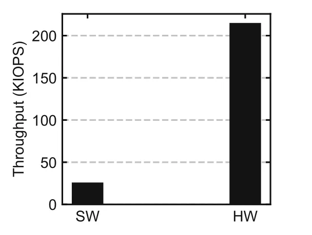
Fig.11 Requests per second of the software (SW)and the hardware (HW) host interface controller implementation
7 Conclusions
In this paper,we propose SoftSSD,which enables rapid prototyping of flash firmware on a real hardware platform.The key technique for achieving this is that we implement the majority of components in pure software so that SoftSSD can provide better observability of the internal states in the SSD,and new storage protocol features can be integrated into the flash firmware without modifying the hardware components.We conduct experiments with real I/O workloads to demonstrate the performance of Soft-SSD as a standard NVMe SSD.We believe that the observability and extensibility provided by the Soft-SSD platform can contribute to future flash firmware development in the research communities.
Contributors
Jin XUE designed the research.Renhai CHEN and Tianyu WANG designed the experiment platform.Jin XUE processed the data,and drafted the paper.Tianyu WANG helped organize the paper.Jin XUE,Tianyu WANG,and Zili SHAO revised and finalized the paper.
Compliance with ethics guidelines
Zili SHAO is a guest editor of this special feature,and he was not involved with the peer review process of this manuscript.Jin XUE,Renhai CHEN,Tianyu WANG,and Zili SHAO declare that they have no conflict of interest.
Data availability
The data that support the findings of this study are available from the corresponding author upon reasonable request.
 Frontiers of Information Technology & Electronic Engineering2023年5期
- Frontiers of Information Technology & Electronic Engineering的其它文章
- Supplementary materials for
- Design and application of new storage systems
- Stacked arrangement of substrate integrated waveguide cavity-backed semicircle patches for wideband circular polarization with filtering effect*
- Modulation recognition network of multi-scale analysis with deep threshold noise elimination*#
- COPPER:a combinatorial optimization problem solver with processing-in-memory architecture*
- DDUC:an erasure-coded system with decoupled data updating and coding*