
Temperature characterizations of silica asymmetric Mach–Zehnder interferometer chip for quantum key distribution
2023-02-20 13:14:02DanWu吴丹XiaoLi李骁LiangLiangWang王亮亮JiaShunZhang张家顺WeiChen陈巍YueWang王玥HongJieWang王红杰JianGuangLi李建光XiaoJieYin尹小杰YuanDaWu吴远大JunMingAn安俊明andZeGuoSong宋泽国
Chinese Physics B 2023年1期
Dan Wu(吴丹), Xiao Li(李骁), Liang-Liang Wang(王亮亮), Jia-Shun Zhang(张家顺),†,Wei Chen(陈巍), Yue Wang(王玥), Hong-Jie Wang(王红杰), Jian-Guang Li(李建光),Xiao-Jie Yin(尹小杰), Yuan-Da Wu(吴远大),2,3, Jun-Ming An(安俊明),‡, and Ze-Guo Song(宋泽国)
1State Key Laboratory on Integrated Optoelectronics,Institute of Semiconductors,Chinese Academy of Sciences,Beijing 100083,China
2Center of Materials Science and Optoelectronics Engineering,University of Chinese Academy of Sciences,Beijing 100049,China
3College of Materials Science and Opto-Electronic Technology,University of Chinese Academy of Sciences,Beijing 100049,China
4Laboratory of Quantum Information,CAS,University of Science and Technology of China,Hefei 230026,China
5Wuxi Institute of Interconnect Technology,Co.,Ltd. Wuxi 214000,China
Keywords: quantum key distribution,planar lightwave circuit,temperature characterization,interference visibility
1. Introduction
To eliminate the potential threat to existing cryptographic systems from the emergence of quantum computers based on Shor algorithms,[1]great efforts have been focused on implementing large-scale or even global quantum key distribution(QKD)networks.[2–4]QKD establishes a key by transmitting a single photon over a quantum channel,and its security is based on the physical laws of quantum mechanics combined with the one-time-pad encryption protocol.[5]Since Bennett and Brassard proposed BB84 protocol,[6]various encoding methods have been used to increase the system secure key rate(SKR),such as time-bin,[7]polarization,[8]phase,[9]measurementdevice-independent (MDI),[10]and twin-field.[11]Research has been done on optical fiber QKD in recent years,[12–14]which is a large size and complex control system. The photonic integrated chip has lots of advantages, such as high integration,[15–17]stable chip performance and low cost.Some QKD experiments based on silica planar lightwave circuit(PLC) chips have been reported,[18–20]which achieves the generation of weakly coherent pulse pairs at the Alice and the decoding of quantum states at the Bob.An asymmetric Mach–Zehnder interferometer(AMZI)is used to modulate the phase by changing the refractive index of its arm using the thermooptic effect. The experiment results show that temperature has a large effect on the interference visibility,and the temperature needs to be precisely controlled in order to achieve a higher interference visibility. The interference visibility decreases obviously when the chip’s temperature is changed. Nambu[18]and Li[19]have studied classical and single-photon interference visibility verse temperature based on silica PLC platform,respectively,but the temperature variation range is only about 2.5°C and 4.5°C when the interference visibility is higher than 95%,which does not facilitate the QKD system to adapt to environmental changes. Although Zhang[20]has proposed a hybrid interferometer with high visibility over 20°C range,but the hybrid integration process is more complex.
In addition,the delay time and peak response wavelength of silica PLC AMZI chip will also change with temperature fluctuation. In order to consider the effect of delay time on the interference visibility and the shift of the classical peak wavelength on the location of single-photon interference,it is essential to study the temperature stability.
In this paper, by designing the equal bend waveguides between the long and short arms, the influence of the bend waveguide stress caused by chip manufacturing is reduced,and the temperature tolerance range of the better interference visibility is increased successfully. In addition, the effects of temperature on the delay time and peak response wavelength of the silica PLC AMZI chip are analyzed.
2. Design and fabrication
The AMZI chip with refractive index difference of 2.0%based on silica PLC platform has been designed and fabricated, whose waveguide geometry is 4 μm×4 μm and footprint is 32.5 mm×18.5 mm. The chip’s structure is shown in Fig.1(a). Both the short and long arms of the AMZI have the same four bend waveguides,and the delay line comes from the straight waveguide length difference. Compared to the structure in Fig. 1(b), this new structure eliminates the stresses in the bend waveguides between the two arms, and the stresses mainly come from the straight waveguides with length differences. A thermal-optic phase modulator(TOPM)is set on one of the arms of the MZI and AMZI,respectively. The TOPM1 is used to balance the extra loss generated by the delay line in the AMZI,so that the powers of the output double pulses are balanced,while the TOPM2 is used to modulate the phase.

Fig.1. AMZI chip. Schematic of the encoding/decoding chips that have different designs,including one MZI,one AMZI with 400 ps delay time that(a) the short arm is made up of bend waveguides and straight waveguides; (b) the short arm is made up of straight waveguide. (c) Photograph of the packaged chip.
The chip is fabricated by silica-based PLC technology.The lower cladding layer is firstly obtained by thermal oxidation,followed by plasma-enhanced chemical vapor deposition(PECVD)to form the core. Then photolithographic exposure and inductively coupled plasma(ICP)are used to etch and transfer the waveguide pattern.Afterwards,the upper cladding layer is deposited by PECVD. Finally, the thin film heater is deposited by magnetron sputtering. The input and output facets of the chip are coupled to the single mode fibers(SMF),then electrodes of TOPM1 and TOPM2 are connected to the printed circuit board(PCB)by wire bonding. The photograph of the packaged chip is shown in Fig.1(c).
The temperature of the chip is controlled using a temperature controller(TEC)with an internal thermistor to measure the temperature with an accuracy of 0.01°C and a measurement range of 15.0°C to 65.0°C.Samples A and B have the same structure, which are selected as encoding and decoding chips,respectively.
3. Experimental results and discussion
3.1. Temperature characterization of single photon interference visibility
Considering the influence of temperature on the interference visibility of the chip, the interference visibility is tested by pulse self-interfering method.[19]The experimental setup is shown in Fig.2. The 1550 nm pulse source with a repetition frequency of 50 MHz and a pulse width of 1 ns is applied. A polarization scrambler with the scrambling frequency 2000 Hz is inserted between the pulse source and the chip. The pulse is attenuated to single photon magnitude with an average photon number of 0.1 per pulse by an optical attenuator. Adjusting the voltage of TOPM1 on the chips to keep the same power between long and short arms, the temperature of the chip is scanned from 20°C to 60°C in steps of 0.1°C,and the photons with temperature are recorded.

Fig.2. Experimental setup using self-interfering method. Single-mode fiber(SMF)is in yellow;polarization maintaining fiber(PMF)is in red.
The interference of chip A as the encoding chip and chip B as the decoding chip is measured. The excess loss of the encoding chip and the decoding chip is-10.87 dB and-6.09 dB, respectively, and the coupling efficiency is 87.1%(0.6 dB per facet). The interference curve versus temperature is shown in Figs.3(a)and 3(b),respectively. For the encoding chip, it can be seen that the TE and TM modes are in antiphase and same phase in the vicinity of 22.0°C and 59.5°C,respectively. For the decoding chip,the TE and TM modes are in same phase in the vicinity of 21.8°C.No anti-phase point can be observed owing to the limited temperature range of the TEC control.
The following analysis can explain this phenomenon.The input pulse is decomposed into two components,TE and TM,which are parallel and perpendicular to the base direction,respectively. When the interfering part occurs in the crossover,the photon number can be expressed as

The interference visibility can be derived as

whereN1is the number of photons in the TE modes of the pulse through the short arm and long arm, whileN2corresponds to the TM modes. ΔφTMare the phase delays of the pulse TM modes in both arms, Δφis the modal phase mismatch between the TE and TM modes. When Δφ=2Nπ,the TE and TM modes are in same phase and the corresponding visibility is maximum. When Δφ=(2N+1)πthe TE and TM modes are in anti-phase and the corresponding visibility is minimum.
For chips A and B, the temperatures of the best interference visibility are significantly different, which could be induced by the fabrication process resulting in the different stresses at different locations on the same silicon wafer. Since chips A and B are located in different positions of the same wafer, the stress distribution of the wafer is nonuniform during the manufacturing process. It leads to different stress birefringences for chips A and B, and correspondingly different refractive indexes for the TE and TM modes. According to Eq. (2), the temperature points at which chips A and B meet the in-phase and anti-phase are also different. In the future mass manufacturing,the in-phase and anti-phase temperature points between chips A and B can be achieved by optimizing the process and reducing the internal stress difference in the wafer.

Fig.3.(a)For the encoding chip,interference curves of TE and TM modes at 20.0–30.0°C and 50.0–60.0°C,respectively.(b)For the decoding chip,interference curves of TE and TM modes at 20.0–30.0 °C.

Fig.4. Experimental setup for QKD system.
Through the above experiments, we roughly get the optimal interference temperature ranges of the encoding and decoding chips. In the following sections,we measured the system interference visibility by connecting in sequence a pulse laser,a polarization controller(PC),the encoding chip,a fiber PBS,a VOA,the decoding chip and two single photon detectors (SPDs), as shown in Fig. 4. The pulse source is set at a repetition frequency of 50 MHz and a pulse width of 50 ps.Three time slots per cycle are obtained at the output of the decoding chip. The output interference photons of the middle slot from the decoding chip are recorded by an SPD.
To precisely obtain in the same phase temperature, the temperature of the decoding chip is scanned from 15.0°C to 25.0°C in steps of 0.1°C while the encoding chip is kept at 59.5°C. The curve of interference with temperature is shown in Fig.5(a). The maximum interference visibility is 92.02%when the decoding chip temperature is in the vicinity of 22.7°C.Then keeping the temperature of the decoding chip constant,the temperature of the encoding chip is scanned from 55.0°C to 65.0°C in steps of 0.1°C, as shown in Fig. 5(b).The maximum interference visibility is 92.14% when the encoding chip temperature is in the vicinity of 61.9°C.Because of the instability of the attenuator during the experiment, the curve in Fig.5(b)shows an upward trend, both the minimum and maximum photon counts around 65°C increase. But the same phase temperature point is still around 61.9°C.
防治方法:早期用药剂把蚜虫和灰飞虱消灭在迁飞至玉米田之前。用40%氧化快乐果3 000倍液或50%抗蚜威可湿性粉剂225~300g/hm2对水750~1 125kg/hm2喷雾。
In Fig. 5, only the TE mode was tested. The reason is that the TE and TM modes are in the same phase and the two curves reflect the same temperature values for higher interference visibility.

Fig.5. The interference curve versus temperature: (a) decoding chip;and(b)encoding chip.
In order to obtain the best interference visibility of the system, the temperature of the encoding chip remains at 61.9°C, and the TOPM2’s voltage of the decoding chip is scanned from 0 V to 9 V at different temperature within 18.0°C–33.0°C, and the photon number is recorded with the corresponding voltage. The system interference visibility varies with the temperature of the decoding chip as shown in Fig.6. It can be seen that the maximum interference visibility at the decoding chip temperature of 24°C is 98.2%(with dark counts removed), which is higher than the measured value in Fig.5. One reason is that the multiple temperature scans make both the encoding and decoding chips at the optimal temperature point, and the other reason is that the phases of TE and TM in Eq.(2)are made to be in rigorous agreement to achieve Δφ=2Nπby adjusting the voltage of TOPM2. Therefore,the interference visibility is greater than 95% in the range of 19°C–31°C, which is a wide temperature range of 12°C.Compared to the reference,[19]our new designed chip displays that the temperature range of high interference visibility is wider. It may be due to the fact that the stresses in the bending waveguide are greater than that in the straight waveguide,the stress is diminished in our designed AMZI where the length difference is from the straight waveguide. When the temperature changes, the mode mismatch generated by the stress is decreased accordingly.

Fig.6. Interference curve versus temperature ranging from 18 °C to 33°C.Insert shows inference fringe at the optimal temperature 24.0°C.
3.2. Temperature characterization of delay line
The difference in delay time between the encoding and decoding chips is detrimental to the interference visibility.Temperature-induced change in the effective refractive index of the waveguide results in a variation in the delay time of the AMZI structure. The variation of the delay time Δtis expressed as

whereng=1.47449 is the group refractive index,cis the speed of light in vacuum,Δnand Δlare the change of refractive index and length difference caused by the change of temperature,

The parametersa= 1.02×10⁻⁵K-1[21]andb= 0.5×10⁻⁶K-1[22]are the thermal-optic coefficient and the thermal expansion coefficient of SiO2,respectively. When the temperature rises from 20°C to 60°C,the variation of the delay time Δtis calculated by Eq.(3),which is about 0.119 ps.
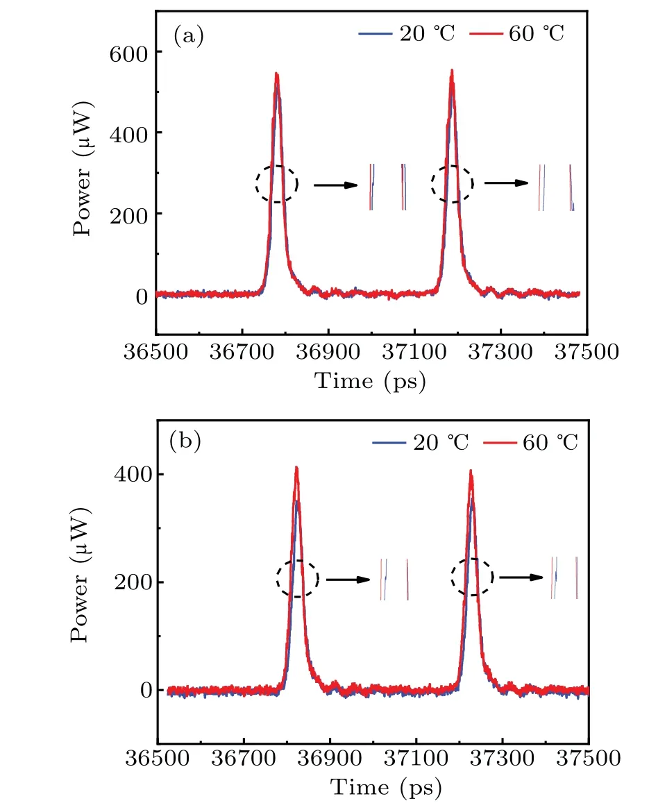
Fig.7. Output waveform from the digital oscilloscope. The delay time of (a) the encoding chip and (b) decoding chip at 20 °C and 60 °C,respectively.
The delay time is measured using pulse laser with a repetition frequency of 50 MHz and a digital oscilloscope. The waveforms of the encoding and decoding chips are recoded at 20°C and 60°C,respectively,as shown in Fig.7.
The delay times of the encoding and decoding chips with temperature are shown in Table 1. It can be seen that the variations of the encoding and decoding chips in delay time are 0.244 ps and 0.321 ps,respectively.

Table 1. Delay time at 20 °C and 60 °C.
For the encoding and decoding chips, the difference of delay time Δt1and Δt2, which is at a certain temperature and changing the same temperature range, respectively, is caused by different stresses at different locations on the same wafer.The discrepancy between the experimental and theoretical analysis is probably caused by the manufacturing process errors of the chip and the thermal stresses from the mismatch in the coefficient of thermal expansion of silica when metal and dielectric materials are integrated to form wiring interconnects on a silicon substrate.[22]

where Δτis the delay time difference between the two chips,Γis the pulse width,A1andA2are the amplitudes of the pulses in the encoding and decoding chips.[23]When the intensities of the two light pulses are equal,the interference visibility can be higher than 98%if the delay time difference between the encoding and decoding chips is less than 14.2 ps. So, the delay time variations of 0.262 ps and 0.339 ps have no impact on the chip interference visibility.
3.3. Tempe rature characterization of CW wavelength response
The interference of the single photon pulse with wavelength 1550 nm of the middle slot at Bob occurs in the BB84 system.Because of the length difference between the two arms of AMZI, the chip is wavelength sensitive. The peak wavelength of the AMZI chip shifts due to the increase of the effective refractive index of waveguide after heating. To eliminate the shift of the peak wavelength so that the interference occurs at 1550 nm, the output response spectra with temperature are analyzed. Since the wavelength of the pulse laser is fixed,the CW laser is used to scan the spectrum to observe the shift. For the AMZI,the phase difference between the two arms is

wherenis the effective refractive index of the waveguide,lis the length difference between the two arms, andφthis the phase difference caused by the TOPM.The light intensity can be expressed as

whereEis the product of the electric vector andE*is the conjugate complex ofE. The optical powers at the input and the output ports of the AMZI areIinandIout,respectively. Considering a particularly narrow wavelength range, ignoring material dispersion and the process error of AMZI in the encoding and decoding chips, ideally the coupling efficiencykof the two DCs in AMZI are equal,which both are 0.5. So,the ratio ofIoutandIinis

The effective refractive index of SiO2varies with temperature as[21]
When the TOPM does not work,φthis equal to zero,according to Eqs.(7)and(10),Eq.(9)can be rewritten as

The variation of normalized powerIout/Iinwith wavelength can be obtained by Eq.(11),as shown in Fig.8(a). The wavelength shift with temperature is about 0.00114 nm/0.1°C.
Then the light from the C-band tunable CW laser is input to the chip and the output power is measured by the optical power meter. When the power of the output double pulse is balanced by adjusting the TOPM1, the extinction ratio of the chip achieves the maximum. The spectra of the decoding chip are scanned in the range of 1549.05 nm to 1550.05 nm at near 24.0°C,as shown in Fig.8(b). The phaseφthis set to zero in Eq.(7),so the phase of the experimental result does not match the phase of the simulation result.

Fig.8. For decoding chip at different temperatures near 24 °C,(a)simulated normalized power versus wavelength, (b) measured loss versus wavelength.
The wavelength shifts of simulation and experiment are shown in Table 2. The measured wavelength shift of the decoding chip is about 0.011 nm/0.1°C,which is in agreement with the simulated result. It can be seen from the simulation and experimental figures that by fine tuning the temperature,the peak response wavelength of the decoding chip can be maintained at 1550 nm without affecting the interference visibility.

Table 1. Wavelength shift with temperature of decoder at 24.0 °C.
4. Conclusion
Silica PLC AMZI chips for QKD with the same bend waveguide in the long and short arms are designed to reduce the effect of bend waveguides stress,and the temperature characterizations are analyzed theoretically and experimentally.The interference visibility is above 95%over a wide temperature range of 12°C.Because of the small thermal-optic coefficient of SiO2,the variation of delay time and the peak wavelength shift are small, which are 0.321 ps within a temperature change of 40°C and 0.0011 nm/0.1°C, respectively. It demonstrates that the chips have high interference visibilities over a wider temperature range,and the temperature has little impact on the delay time,and the peak wavelength of the decoding chip can be maintained at 1550 nm without affecting the interference visibility,which are more tolerant to external environmental temperature variations.
Acknowledgements
Project supported by the National Key R&D Program of China (Grant No. 2018YFA0306403), the Strategic Priority Research Program of Chinese Academy of Sciences (Grant No. XDB43000000), Innovation Program for Quantum Science and Technology,and Computer Interconnect Technology Alliance Funding(Grant No.20220103).
猜你喜欢
四川蚕业(2021年4期)2021-03-08 02:59:56
农技服务(2020年2期)2020-12-18 01:34:28
农药科学与管理(2019年12期)2019-05-20 09:33:28
现代农业(2016年4期)2016-02-28 18:42:10
杂草学报(2015年2期)2016-01-04 14:58:03
营销界(2015年23期)2015-02-28 22:06:18
营销界(2015年23期)2015-02-28 22:06:17
现代农业(2015年5期)2015-02-28 18:40:47
现代农业(2015年5期)2015-02-28 18:40:42
现代农业(2015年3期)2015-02-28 18:40:23
- Chinese Physics B的其它文章
- LAMOST medium-resolution spectroscopic survey of binarity and exotic star(LAMOST-MRS-B):Observation strategy and target selection
- Vertex centrality of complex networks based on joint nonnegative matrix factorization and graph embedding
- A novel lattice model integrating the cooperative deviation of density and optimal flux under V2X environment
- Effect of a static pedestrian as an exit obstacle on evacuation
- Chiral lateral optical force near plasmonic ring induced by Laguerre–Gaussian beam
- Adsorption dynamics of double-stranded DNA on a graphene oxide surface with both large unoxidized and oxidized regions