Effect of surface plasmon coupling with radiating dipole on the polarization characteristics of AlGaN-based light-emitting diodes
Yi Li(李毅), Mei Ge(葛梅), Meiyu Wang(王美玉), Youhua Zhu(朱友华), and Xinglong Guo(郭兴龙)
School of Information Science and Technology&Tongke School of Microelectronics,Nantong University,Nantong 226019,China
Keywords: surface plasmon,AlGaN-based light emitting diodes,FDTD,K-P method
1. Introduction
AlGaN-based light emitting diodes (LEDs) as the deep ultraviolet (DUV) light sources have attracted great attention due to their potential applications in water purification,optical catalysis and other fields.[1]Although great progress has been made in the research of AlGaN-based DUV LEDs,[2]the luminous efficiency is still lower than that of GaN-based visible LEDs.[3]One of the limiting factors to improve the luminous efficiency of DUV-LEDs is the poor light extraction efficiency(LEE).Different from GaN material,the crystal-field split-off hole(CH)band of AlGaN alloy will become the topmost valence subband with the increase of Al-content,[4]which will lead to the transverse-magnetic (TM) dominated emission.[5]The TM polarization denotes that the emission polarization is perpendicular to thec-plane. Forc-plane AlGaN-based LEDs,TM polarized emission is difficult to extract from the top or bottom surface. In addition,due to the low conductivity of p-AlGaN,the p-GaN contact layer is often employed in AlGaNbased DUV-LEDs, which will lead to strong absorption and reduce the LEE of the device.[6]
In order to improve the performance of DUV LEDs,structural design strategies are often used, such as ultrathin GaN/AlN multiple quantum well (MQW) structure[7]and lateral-polarity structure.[8]Moreover, an alternative method is to adopt the surface plasmon (SP) coupled LED structure, which can enhance both the internal quantum efficiency(IQE) and LEE.[9]For example, Heet al.reported that the IQE and LEE of DUV LED with Al nanoparticles (NPs) on SiO2dielectric interlayer were increased by 230% and 13%,respectively.[10]Interestingly, Zhanget al. reported that the enhancement ratio of transverse-electric(TE)mode was larger than that of TM mode through local SP (LSP) coupling,[11]which will help to improve the luminous efficiency ofc-plane LED devices. The TE polarization denotes that the polarization is parallel to thec-plane. The corresponding mechanism was considered that the LSP–QW coupling results in the conversion of some TM emission to TE emission. However, detailed theoretical analysis is lacking in the literature.
In this study,we focus on the effect of SP coupling on the polarization characteristics of DUV LEDs by numerical calculation.Firstly,considering the valence band mixing effects and the scattering relaxation, the TE/TM polarized spontaneous emission (SE) rate into the SP mode are calculated by 6×6 K-P method.[12]The corresponding band structure is obtained by self-consistent solution of Schr¨odinger–Poisson equations.Then,the scattering process of radiating dipole with TE mode or TM mode in the metal nanostructures is investigated by the three-dimensional(3D)finite-difference time-domain(FDTD)simulation. Thus,the effect of the radiative recombination by SP–QW coupling and the scattering by metal nanostructures on the TE/TM polarized emissions can be described, respectively. Through these simulation results, the influence of SP coupling behavior on the optical anisotropy of AlGaN-based LEDs can be better understood.
2. Theory
When an electron-hole pair in the AlGaN QW is located within the SP fringing field penetration depth, the radiative recombination energy can be transferred into the SP mode instead of into the free space.[13]The corresponding SE rate into the SP mode can be expressed as[12]

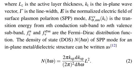
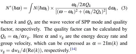
Here,kspandL2are the real part of wave vector and the inplane area, respectively. As taking account to ohmic loss of metal materials,the DOS of SPP mode will be broadened.[14]The modified DOS can be expressed as
For TE polarized emission, the momentum matrix element|E·pσnm|2in formula(1)can be written as[12]

Meanwhile,for TM polarized emission,the momentum matrix element is
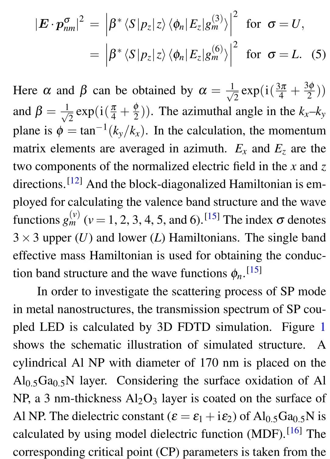
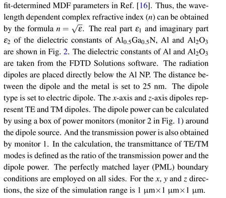
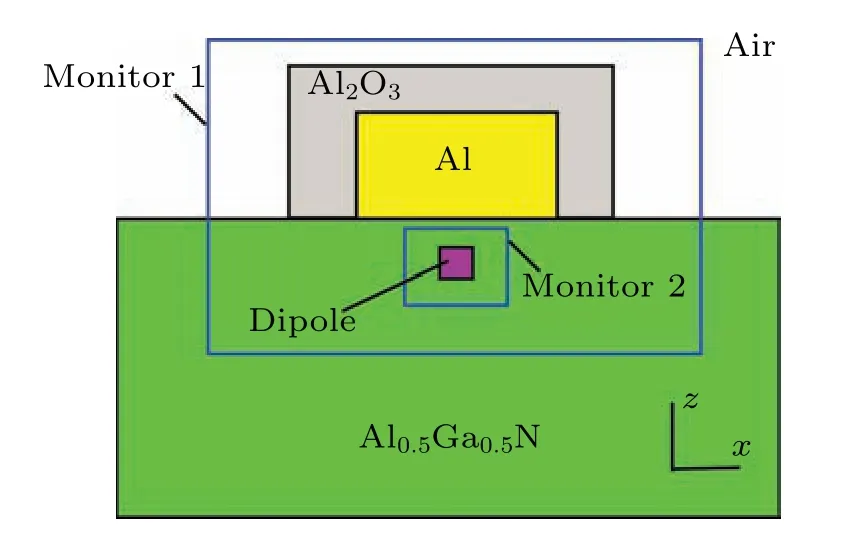
Fig.1. Schematic illustration of simulated structure.
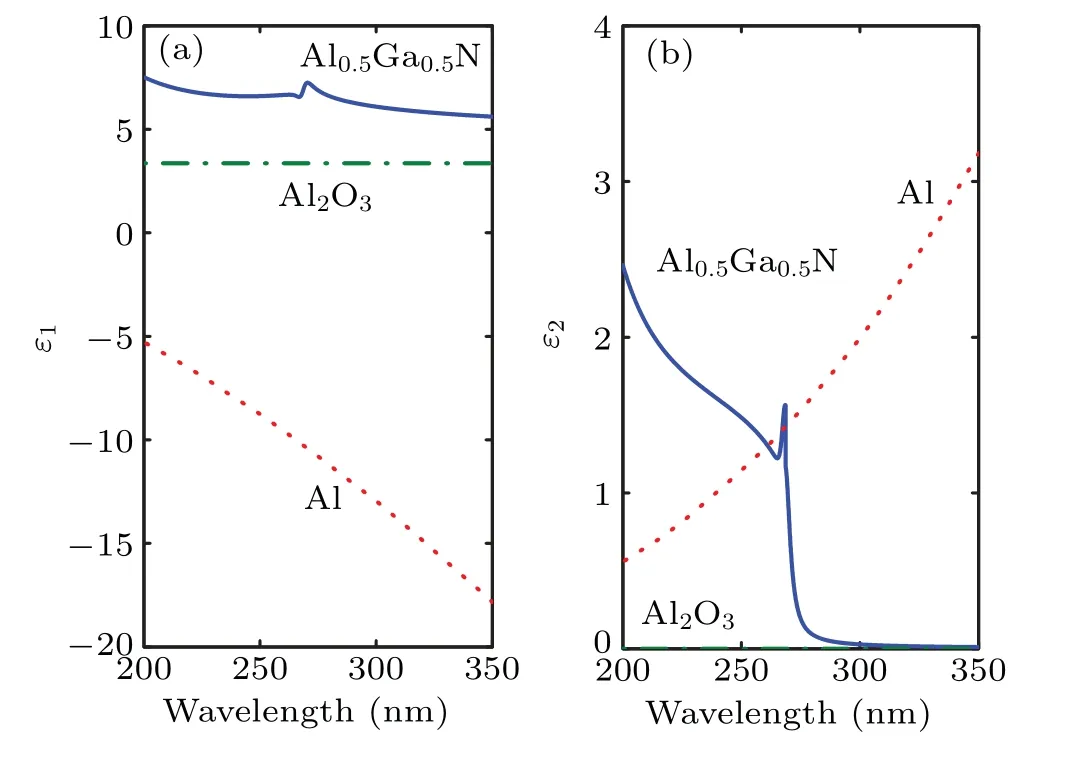
Fig. 2. The real part ε1 (a) and imaginary part ε2 (b) of the dielectric constants of Al0.5Ga0.5N,Al and Al2O3.
3. Results and discussion
3.1. DOS and normalized electric field of SPP mode
Figure 3 shows the schematic diagram of the Al0.5Ga0.5N/Al/Al2O3slab structure and the dispersion relation of SPP modes with different Al thickness. The dispersion relation of the SPP mode is calculated by performing a parameter sweep over the wave vectorkspand looking for frequencies with strong resonances. In the calculation, the two-dimensional(2D)FDTD simulation is used. The dimension of the simulation range is 2 μm×1 nm for thezandxdirections. The PML boundary condition is set in thezdirection and the Bloch boundary condition is set in thexdirection.Ten randomly oriented dipoles are set in the simulation region.In Figs.3(b)and 3(c),two SPP modes from the AlGaN/Al and Al/Al2O3interfaces can be observed. In the regime of small wave vectorsksp, the dispersion curves from the AlGaN/Al interface are close to the light lines, and the waves can extend into the dielectric space. Therefore, SPPs are known as Sommerfeld–Zenneck waves in this regime.[17]In the regime of large wave vectors, the SPP mode from the AlGaN/Al interface approaches the SP“resonance”energy(ESP≈4.6 eV)asymptotically. For the thinner Al layer, the dispersion curve deviates slightly farther from the resonance energy due to the strong interaction of SPP modes in the two interfaces. In fact,when the thickness of Al is 50 nm,the dispersion curve almost coincides with that of semi infinite thickness Al film. The dotted lines in Figs.3(b)–3(d)are the SPP dispersion relation of AlGaN/Al/air structure,which is calculated by the formula[13]

Hereε1,ε2,andε3are the permittivity of AlGaN,Al,and air,respectively.tis the thickness of Al film. It can be seen from the figure that the calculated results are basically consistent with the FDTD fitting result. That is to say, the influence of 3nm-thick Al2O3on the dispersion relation of SPP can be ignored.It should be noted that since the imaginary part of wave vectorkis difficult to obtain from FDTD simulation, we use the dispersion relation calculated by formula(6)when calculating the modified DOS of SPP mode. Figure 4 shows the modified DOS of SPP modes from the AlGaN/Al interface.For the Al0.5Ga0.5N/Al/Al2O3slab with different Al thickness,the modified DOS of SPP mode has a maximum value at 4.4–4.48 eV. The energy corresponding to the peak DOS of SPP mode is lower than the SP resonance energy,which can be attributed to the larger imaginary part of the wave vector at the SP resonance. In addition,compared with other Al film thickness,the peak DOS of 50 nm thick Al film is relatively large.
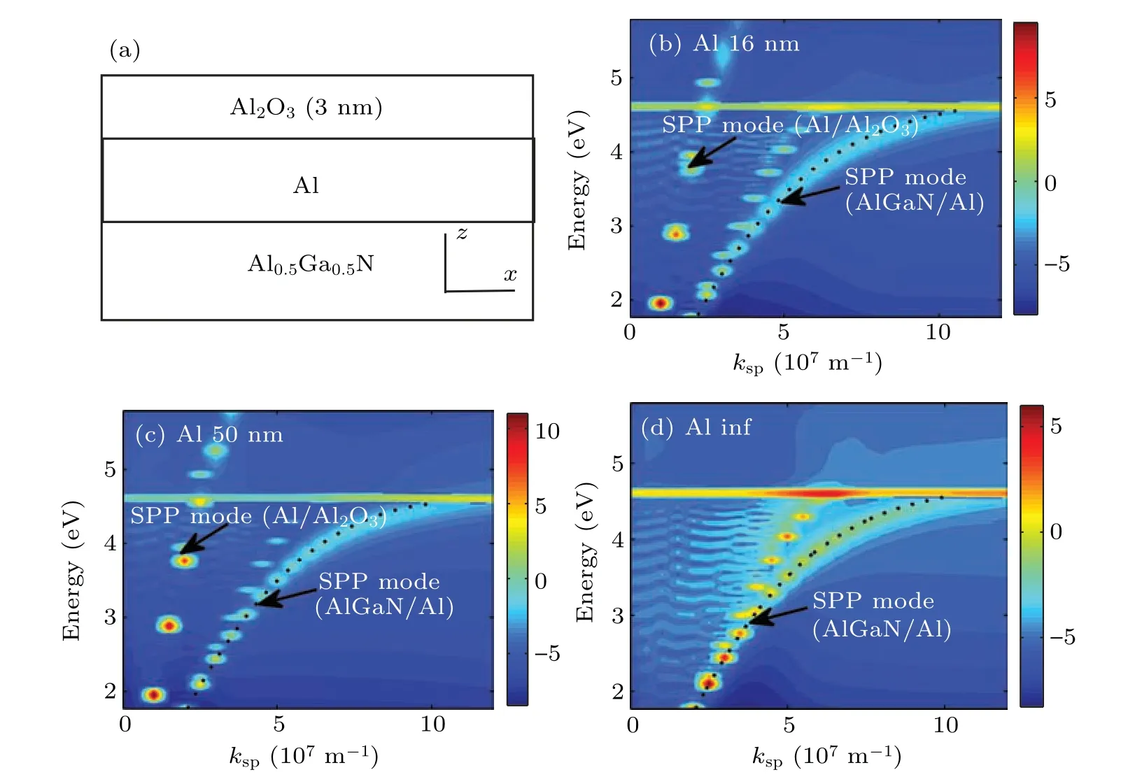
Fig.3. (a)Schematic diagram of the Al0.5Ga0.5N/Al/Al2O3 slab structure and the dispersion relation of SPP modes with(b)16 nm Al film,(c)50 nm Al film,and(d)infinite thickness Al film.
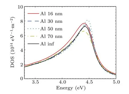
Fig. 4. The modified DOS from the AlGaN/Al interface for the Al0.5Ga0.5N/Al/Al2O3 slab with different Al thickness.
Figure 5 shows the normalized electric field(Ex,Ez)with infinite thickness Al film, 50 nm Al film, 30 nm Al film, and 16 nm Al film from 2D FDTD simulation. The dimension of the simulation range is 1 μm×2 μm for thezandxdirections. The PML boundary conditions are set in the both directions. In order to eliminate the influence of“magnetic dipole”light source on detecting the electric field of SPP mode,a high absorption material is used to separate the light source from the monitor in the simulation. Only 4 nm gap are left to pass through the excited SPP mode from the AlGaN-Al interface.In Fig. 5(a), the normalized electric field solved analytically is also shown. The corresponding un-normalized electric field from the AlGaN–Al interface is calculated by the following formula:[18]
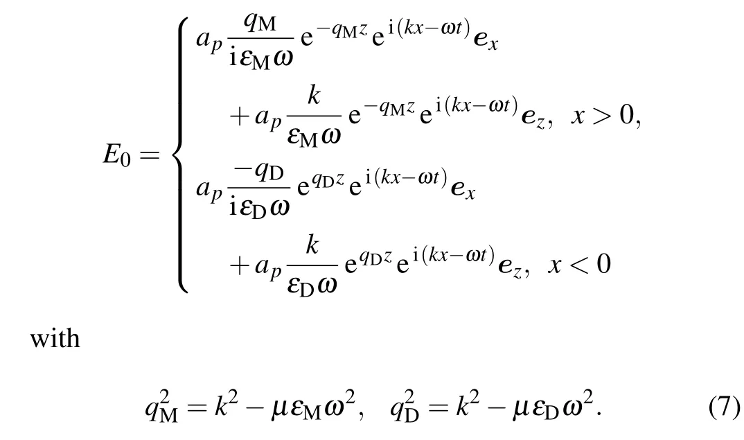
Here,the subscripts M and D denote Al and AlGaN materials,respectively. From Fig.5(a),it can be seen that the FDTD fitting result is basically consistent with the analytical solution result. In addition, the SPP evanescent field decays exponentially. It can be seen from the figure that the evanescent field on the AlGaN side is almost 0 at a distance of 50 nm from the metal aluminum. The short SP coupling distance will become the difficulty in the practical preparation of SP coupled LED devices. With the decrease of Al layer thickness,the field intensity on AlGaN side decreases obviously due to the coupling of SPP modes from the two interfaces of Al layer. At the same time,the influence of the light source on the detected field distribution is more significant, so that the evanescent field on the AlGaN side of the structure with Al thickness of 16 nm will not be exponentially reduced to 0,as shown in Fig.5(d).Moreover,as Al thickness is decreased to 16 nm,it is also observed that theExcomponent of the normalized electric field on the AlGaN side is greater than theEzcomponent, which means that the SE rate of TE polarization will be greater than that of TM polarization.
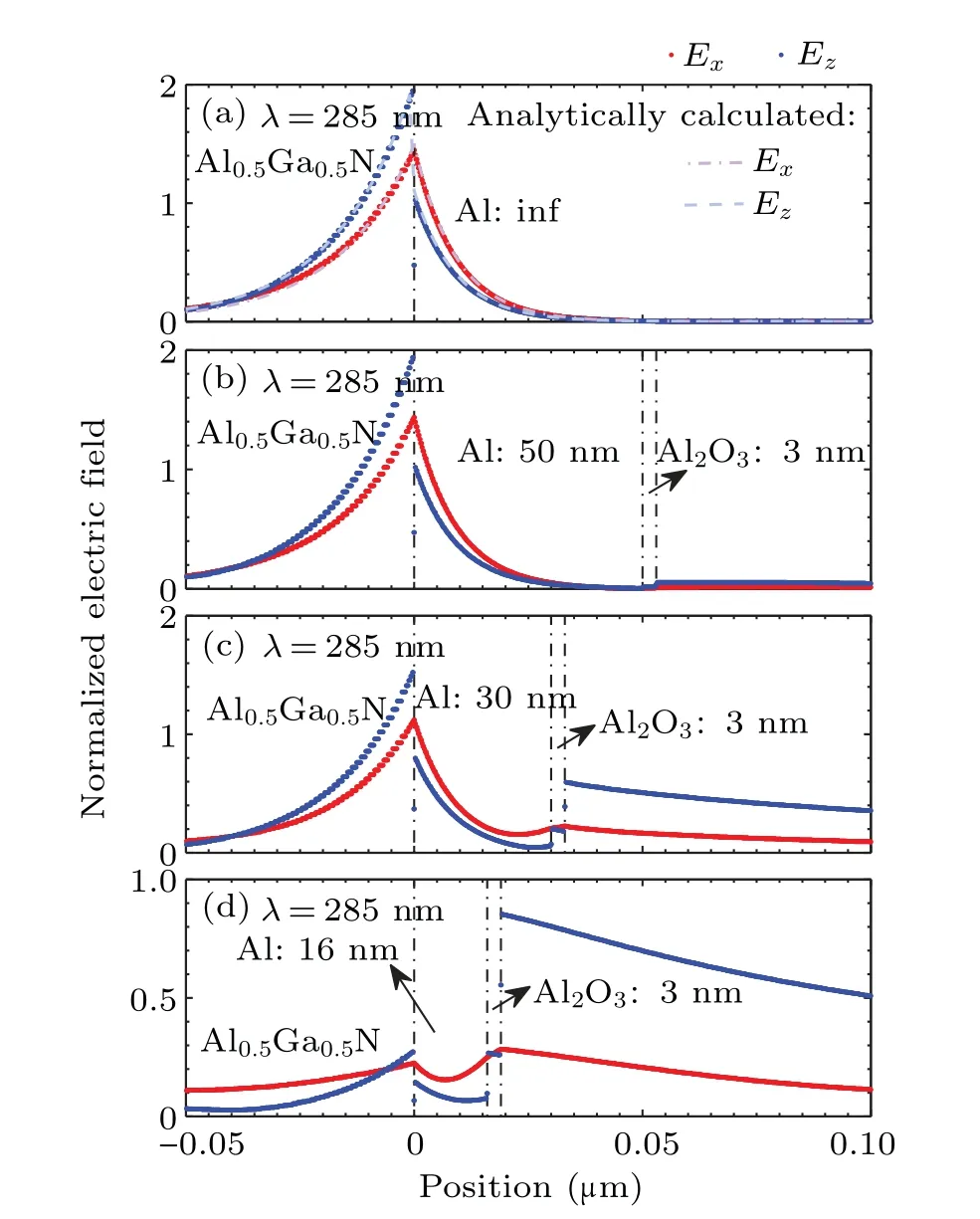
Fig.5. The normalized electric field with(a)infinite thickness Al film,(b)50 nm Al film,(c)30 nm Al film,and(d)16 nm Al film.
3.2. SE rate into SPP mode
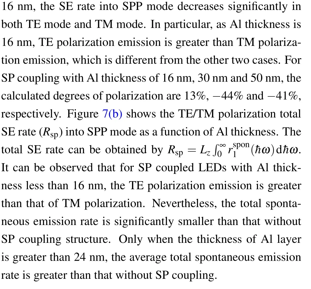
By using the DOS and normalized electric field obtained above,the TE/TM polarized SE rate into the SPP mode is calculated. Here,the radiation dipole is considered to come from a quantum well structure composed of a 2 nm Al0.35Ga0.65N well layer and an 8 nm Al0.5Ga0.5N barrier layer. The band structure is calculated by the 6×6 K-P method. The sheet carrier density is set as 8×1012cm-2.Figure 6 shows the TE/TM polarized spontaneous emission spectra from the SP–QW coupling. The thickness of Al is set to be infinite. The spacingdbetween QW and Al is set to be 15 nm and 25 nm. Compared with the case without SP coupling,the SE rate into SPP mode is significantly improved regardless of TE polarized emission or TM polarized emission. However, the degree of polarization (DOP) decreased from-14% without SPP coupling to-44% (d=15 nm) and-42% (d=25 nm). The DOP is defined asρ=(ITE-ITM)/(ITE+ITM).ITEandITMare the integrated intensity of the TE-polarized and TM-polarized SE rate into SPP mode or free space.
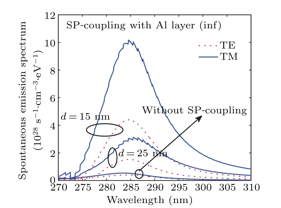
Fig. 6. TE/TM polarized spontaneous emission spectra from the SP–QW coupling. The thickness of Al is set to infinite. The spacing d between QW and Al is set to be 15 nm and 25 nm. The spontaneous emission spectrum without SP coupling is also shown.
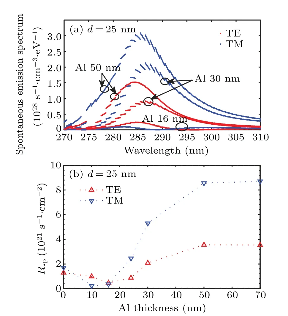
Fig.7.(a)TE/TM polarized spontaneous emission spectra from SP coupling with Al thickness of 16 nm, 30 nm, and 50 nm; (b) the TE/TM polarization total SE rate(Rsp)into SPP mode as a function of Al thickness. The Rsp into free space without SP coupling is also shown in(b).

3.3. Transmittance for Al NP structure
It is shown above that the DOP of SP coupled LED varies with Al thickness. However,due to the anisotropic extraction behavior of polarized light,[19]the actual DOP will be different from the above calculation results. Figure 8(a)shows the transmission spectra of an Al NP placed on the Al0.5Ga0.5N layer. The structure diagram of the simulation is shown in Fig.1. It can be obviously observed that the transmittance of TE-polarized light is much larger than that of TM-polarized light,which will lead to greater DOP.Compared with the case without SP coupling, the ratio of transmittance between TE polarization and TM polarization through SP coupling is significantly improved. Figure 8(b)shows the transmittance as a function of Al thickness atλ=285 nm. When the thickness of Al is less than 20 nm, the transmittance of TM polarization decreases significantly faster than that of TE polarization with the increase of Al thickness. When the thickness of Al is greater than 20 nm, the transmittance of both TE/TM polarizations basically remains unchanged with the increase of Al thickness. With the increase of Al thickness from 0 nm to 70 nm,the ratio of transmittance between TE polarized emission and TM polarized emission increases from 1.2 to 7.8. It should be noted that the position of radiation dipole can significantly affect the calculated TE/TM polarized light transmission ratio. For example, when the dipole moves from directly below Al NP to the edge, the ratio for the 30 nm Al NP structure decreases from 7.5 to 1.82. Nevertheless,the ratio of average transmittance of TE/TM polarized light can still reach 3.06. As a result, the DOP of SP coupled LED can be expected to be improved in the actual applications,as reported in Ref.[11].
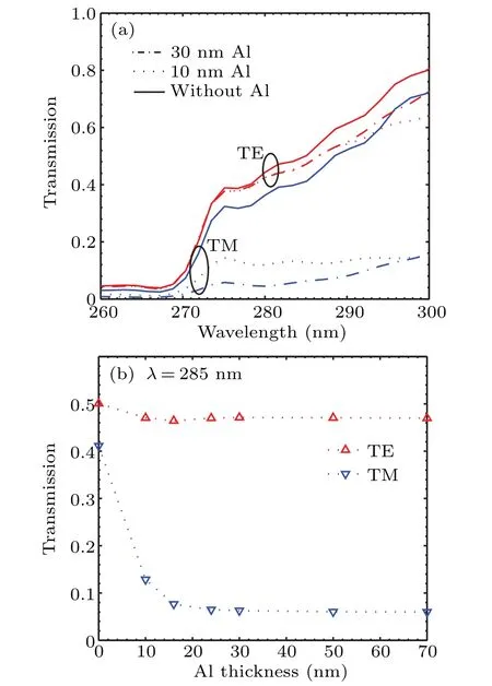
Fig. 8. (a) The transmission spectra of an Al NP placed on the Al0.5Ga0.5N layer; (b) the transmittance as a function of Al thickness at λ =285 nm.
4. Conclusion
In summary,the optical anisotropy of SP coupled LED is studied by 6×6 K-P method and FDTD simulation. Through SP coupling, the energy of the radiation dipole can be transferred to the SPP mode,which can be expected to improve the radiation recombination rate of LED devices. However, the dipole-SP coupling has different effects on TE/TM polarized emission. For the Al0.5Ga0.5N/Al/Al2O3slab structure,when the thickness of Al is less than 16 nm,the TE-polarized SE rate into SPP mode is significantly higher than that of TM mode due to the largerExcomponent of the normalized electric field on the AlGaN side. At the same time, when Al thickness is greater than 24 nm,TM polarized emission becomes the dominant emission, and the average total SE rate is greater than that without SP coupling. For the Al NPs structure,the extraction behavior of TE/TM polarized light is obviously different.Compared with the structure without Al,the decrease of transmittance of TM polarized light is much greater than that of TE polarized light. Thus, the ratio of transmittance between TE polarization and TM polarization for the 30 nm Al NP structure can be increased by 1.55 times atλ=285 nm.In practical application,the reasonable design of SP coupled LED device can significantly improve the DOP and luminous efficiency.
Acknowledgements
This work was supported by the National Nature Science Foundation of China (Grant Nos. 62004109, 61874168, and 62074086),Jiangsu Provincial Double-Innovation Doctor Program,Development of antibacterial multifunctional PVC facing new material technology(Grant No.21ZH626).
- Chinese Physics B的其它文章
- Solutions of novel soliton molecules and their interactions of(2+1)-dimensional potential Boiti–Leon–Manna–Pempinelli equation
- Charge density wave states in phase-engineered monolayer VTe2
- High-pressure study of topological semimetals XCd2Sb2(X =Eu and Yb)
- Direct visualization of structural defects in 2D semiconductors
- Switchable down-,up-and dual-chirped microwave waveform generation with improved time–bandwidth product based on polarization modulation and phase encoding
- Machine learning potential aided structure search for low-lying candidates of Au clusters

