Charge density wave states in phase-engineered monolayer VTe2
Zhi-Li Zhu(朱知力), Zhong-Liu Liu(刘中流), Xu Wu(武旭)2,, Xuan-Yi Li(李轩熠),Jin-An Shi(时金安), Chen Liu(刘晨), Guo-Jian Qian(钱国健), Qi Zheng(郑琦),Li Huang(黄立), Xiao Lin(林晓), Jia-Ou Wang(王嘉欧), Hui Chen(陈辉), Wu Zhou(周武),Jia-Tao Sun(孙家涛)2,, Ye-Liang Wang(王业亮)2,,†, and Hong-Jun Gao(高鸿钧),‡
1Institute of Physics and University of Chinese Academy of Sciences,Chinese Academy of Sciences,Beijing 100190,China
2MIIT Key Laboratory for Low-Dimensional Quantum Structure and Devices,School of Integrated Circuits and Electronics,Beijing Institute of Technology,Beijing 100081,China
3Institute of High Energy Physics,Chinese Academy of Sciences,Beijing 100084,China
Keywords: charge density wave,H-VTe2,phase engineering,transitional metal dichalcogenides
1. Introduction
As a collective phenomenon of great interest in condensed matter physics, charge density wave (CDW)[1]is discovered in many transitional metal dichalcogenides(TMDs).[2]In this group of two-dimensional (2D) materials with diverse components and unique properties, the CDW transition not only reflects diverse spatial and electronic structure with complicated origins,[3–6]but also exhibit great potential for applications.[7–12]For the required manipulation,phase engineering[13]is an effective method to modify both the structural and electronic properties of TMDs,[14,15]including CDWs.[14,16]Such manipulation usually requires energy to overcome the barrier between different phases.[15,17,18]Thus,phase engineering is more effective on a TMD material with a smaller formation energy difference between phases.
Among TMDs, vanadium dichalcogenides (VX2,X=S,Se, Te) are drawing tremendous attention recently and have been reported with several unexpected CDW states and electronic properties.[19–27]According to the previous calculation results,[28–31]T and H-phase VX2share very similar forming energy, especially for VTe2, meaning a high possibility for phase engineering. The experimental reports of CDW in VTe2are focused on its T-phase,which is the stable phase in its bulk.However,the report on CDW states of H-VTe2is still rare,in spite of the intense theoretical calculations.[30–35]

2. Experimental section
2.1. Sample preparation
The sample of monolayer T-VTe2on epitaxial graphene on silicon carbide(Gr/SiC)was fabricated in an ultrahigh vacuum(UHV)chamber with the base pressure of 4×10⁻¹⁰mbar(1 bar=105Pa), which was equipped with standard MBE facilities. The Gr/SiC substrate was prepared by annealing the doped SiC crystalline substrate (TankeBlue) at 1500 K for 40 minutes after degassing at 900 K for 1 hour. Vanadium (ESPI Metals, 99.999%) atoms and tellurium (Sigma,99.999%)atoms were deposited on Gr/SiC substrate from an electron-beam evaporator and a Knudsen cell, with the substrate temperature of 510 K. The grown process was under Te-rich condition, aiming to guarantee that enough Te atoms react with V atoms. And the growth rate of T-VTe2on Gr/SiC is about one layer per hour. Partial transformed H-VTe2was obtained by annealing T-VTe2at 530 K for 40 minutes in an ultrahigh vacuum condition.
2.2. XPS measurements
Thein-situx-ray photoelectron spectroscopy measurements of as-grown and annealed samples were performed in the Beijing Synchrotron Radiation Facility (BSRF). Synchrotron radiation light, which was monochromated by four high-resolution gratings and controlled by a hemispherical energy analyzer,has photon energy from 10 eV to 1100 eV.
2.3. STEM measurements
Before STEM measurements, we firstly deposited 10-nm C60and 50-nm Sb on as-grown T-VTe2and partial transformed H-VTe2on Gr/SiC,aiming to protect the sample from oxidation and damage. Then the samples were sliced along SiC(1120) face by a focused ion beam (FIB) and were further thinned to around 40-nm thickness using low-energy ion milling. And the cross-section high-angle annular dark-field scanning transmission electron microscopy(HAADF-STEM)images were obtained with an aberration-corrected STEM operated at 100 kV.
2.4. STM and LEED measurements
All thein-situSTM measurements were carried out in ultrahigh vacuum condition, with a base pressure under 4×10⁻¹⁰mbar, in the constant-current mode, at room temperature(RT)(300 K)and 4.5 K.Thein-situLEED characterizations were carried out by an Omicron LEED system,with the base pressure under 4×10⁻¹⁰mbar.The results were obtained with the electron energy of 40 eV.
2.5. ARPES measurements
ARPES measurements were performed at the photoelectron spectroscopy end station of the Beijing Synchrotron Radiation Facility 4B9B beamline. The experiments used He I(hν=21.2 eV) resonance lines and a VG SCIENTA R4000 analyzer with the instrument energy resolution was better than 30 meV,and the angular resolution was 0.3°.All the data were recorded in UHV(better than 3×10⁻¹⁰mbar,1 bar=105Pa)at room temperature.
2.6. DFT calculations
The first-principles calculations for the geometry optimization and electronic structures of VTe2monolayers are performed by using the Viennaab initiosimulation package (VASP).[36]The projector augmented wave (PAW)[37]pseudopotentials and the generalized gradient approximation(GGA)exchange–correlation functionals proposed by Perdew,Burke,and Ernzerhof(PBE)[38]are used. The 11×11×1kpoint grid is used in geometry optimization with a free energy tolerance of 10-5eV and a force tolerance of 0.01 eV/˚A.Spinorbit coupling is included when calculating the band structures. A vacuum of 25 ˚A is adopted to avoid the vertical direction interactions between periodic layers.
2.7. Results and discussion
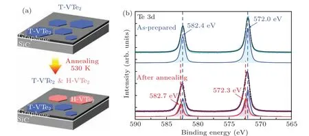
High-quality monolayer T-VTe2was fabricated on Gr/SiC substrate in an ultrahigh vacuum chamber through coevaporating of V and Te atoms with the substrate temperature of 510 K(see Sample preparation). And with further annealing of the as-grown sample at 530 K for 40 min,T-VTe2will partially transform to H-VTe2, as shown in Fig. 1(a). The XPS characterization results of as-grown and annealed samples in Fig. 1(b) show that the binding energy of Te 3d5/2 and 3d3/2 for the as-grown sample is 572.0 eV and 582.4 eV,agreeing with previous work about T-VTe2.[27]While,there is another set of peaks at 572.3 eV and 582.7 eV for annealed sample,which shows an energy shift of 0.3 eV to the T-VTe2peaks. This extra set of peaks implies an emergent new phase of VTe2.
To characterize the atomic structure of the emergent phase, we performed cross-section STEM measurements on the T-VTe2and T/H-VTe2samples. As shown in Figs. 2(a)and 2(d),the T and H phase VTe2can be clearly distinguished from the side view of the atomic model. In the STEM results shown in Figs. 2(b) and 2(e), the cross-section image of the VTe2, corresponding to the side view atomic model, reveals the structure of T and H-VTe2unambiguously. From the line profiles shown in Figs. 2(c) and 2(f), we can read the size of the marked unit cell is 0.31 nm and 0.32 nm for T and H-VTe2,respectively. Then, we can calculate that the lattice constant of T and H-VTe2is 0.35 nm and 0.36 nm,respectively. Thus,we prove that the phase-engineering of monolayer VTe2can be performed from T to H-phase through a transition process by annealing, demonstrated by the combination of XPS and cross-section STEM results.


Fig. 1. XPS results of T-VTe2 and T/H-VTe2 samples. (a) Schematic diagram of the fabrication of the T/H-VTe2 sample on the graphene substrate.(b)The Te 3d spectra of the T-VTe2 (as-prepared)and T/H-VTe2 sample(after annealing). The Te 3d peak positions(of pure T-VTe2 at 582.4 eV and 572.0 eV,of T/H-VTe2 mixture at 582.7 eV and 572.3 eV),showing an energy shift of 0.3 eV.

Fig.2. The cross-section STEM results of T-and H-VTe2. (a)and(d)The atomic models of T(a)and H-VTe2 (d)in side view(upper)and top view(lower). (b)and(e)The cross-section HAADF-STEM images of T(b)and H-VTe2(e). The unit cells in side view are marked with black dashed frames.(c)and(f)The line profiles along the blue and red arrows in panels(b)and(e),respectively.
Moreover, atomic resolution STM measurements were carried out to reveal the CDW superlattice, to further characterize the atomic structure of the monolayer VTe2. The zoomin atomic resolution STM image, the corresponding line profile,and the fast Fourier transform(FFT)pattern of monolayer T-VTe2, as shown in Figs. 4(a)–4(c), demonstrate the hexagonal atomic lattice with 0.35-nm lattice constant, without any superstructure. The angle-resolved photoemission spectroscopy(ARPES)results also reveal the electronic structure,which is the same as calculated(See Fig.S1 in Supplementary information)and previous reports.[25–27]These results agreed with its LEED pattern at RT in Fig. 3(c). As a comparison,the atomic resolution STM image of T-VTe2at 4.5 K is shown in Fig. 4(d), which clearly displays a superlattice, as the reported CDW pattern of T-VTe2below 186 K.[23,25–27]The line profile shown in Fig.4(e)reveals the period of the CDW pattern is 1.42 nm. Combined with the 4×4 superlattice in the FFT pattern shown in Fig. 4(f), we can calculate the lattice constant of 0.35 nm, which agrees with the STM and STEM results mentioned above.


Fig. 3. Room-temperature STM and LEED results of the T-VTe2 and T/H-VTe2 samples. (a) and (d) STM topographic images (-2.0 V, 200 pA)of T-VTe2 (a) and H-VTe2 (d) islands, respectively. (b) and (e) Line profiles along the blue and red lines in panels (a) and (d), respectively. (c) and(f) LEED patterns of the T-VTe2 and T/H-VTe2 sample. The diffraction spots of T-VTe2 (aT), T/H-VTe2 (aH), H-VTe2 superlattice (23aH) and its secondary diffraction spots are marked with the blue,purple,red and yellow dotted circles,respectively.

Fig.4. Atomic-resolution STM images of T-VTe2. (a)and(d)Atomic-resolution STM images of T-VTe2 measured at 300 K(-0.1 V,1 nA)(a)and 4.5 K(-50 mV,1.5 nA)(d),respectively. The atomic lattice and CDW superlattice are depicted with white and blue dashed rhombus,respectively. (b)and (e) Line profiles along the white and blue dashed arrows in panels (a) and (d), respectively. (c) and (f) The FFT patterns of the STM images in panels(a)and(d),respectively. The spots of the atomic lattice at 300 K,4.5 K,and the CDW superlattice are marked with black,purple,and blue dotted circles,respectively.

Fig.5. CDW superlattice of H-VTe2. (a)Atomic-resolution STM image(0.1 V,2 nA)of H-VTe2 measured at 300 K.The unit cell of CDW superlattice is depicted with the yellow dashed rhombus. (b)Line profile along the white dashed arrow in panel(a). (c)The FFT pattern of the image in panel(a).The spots of the H-VTe2 atomic lattice and CDW superlattice are marked with purple and red dotted circles, respectively. (d)and(e)LEED patterns of the T/H-VTe2 measured at 400 K and 450 K,respectively. The spots of the T/H-VTe2 lattice and CDW superlattice are marked with purple and reddotted circles,respectively.
The Fermi-surface nesting[39]and the electron–phonon coupling[20,25]are the two common theories used to explain the origin of CDW in 2D TMDs. In the previous ARPES investigation of monolayer T-VTe2, the CDW behavior in such a 2D layer was attributed to the Fermi-surface nesting of its anisotropic gaped Fermi contour.[25]While other observations by STM and STS mapping suggested that there could be other mechanisms contributing to VTe2’s CDW, which leads to the breaking of its three-folder symmetry. In the H-VTe2case,the CDW behavior becomes further complicated with the extreme robustness via temperature,which further indicates that mechanism other than Fermi-surface nesting and electron–phonon coupling is involved in the origin of its CDW. Moreover, in contrast with other TMDs, such as H-TaSe2,[40]T-TiSe2,[41]and T-VSe2,[22]the higher CDW transition temperature of HVTe2resembles those of the mott-insulating T-NbSe2[42–44]and T-TaS2,[4,45,46]in which the electron correlation take dominance. Whether some sort of electron correlation contributes to the origin of H-VTe2’s CDW still requires further investigation,but nevertheless,monolayer H-VTe2provides an ideal platform for exploring the mechanism behind the complicated CDWs in 2D-TMD systems.
3. Conclusion and perspectives

Acknowledgements
Project supported by the National Key Research and Development Program of China(Grant Nos.2021YFA1400100,2020YFA0308800,and 2019YFA0308000),the National Natural Science Foundation of China (Grant Nos. 92163206,62171035, 62171035, 61901038, 61971035, 61725107,and 61674171), the Beijing Nova Program from Beijing Municipal Science & Technology Commission (Grant No. Z211100002121072), and the Beijing Natural Science Foundation(Grant Nos.Z190006 and 4192054).
- Chinese Physics B的其它文章
- Solutions of novel soliton molecules and their interactions of(2+1)-dimensional potential Boiti–Leon–Manna–Pempinelli equation
- High-pressure study of topological semimetals XCd2Sb2(X =Eu and Yb)
- Direct visualization of structural defects in 2D semiconductors
- Switchable down-,up-and dual-chirped microwave waveform generation with improved time–bandwidth product based on polarization modulation and phase encoding
- Machine learning potential aided structure search for low-lying candidates of Au clusters
- Switchable and tunable triple-channel bandpass filter

