
Rational self-assembly of polygonal organic microcrystals for shape-dependent multi-directional 2D optical waveguides
2022-07-11 03:39ChoFeiXuYueYuQingLvChngCunYnXueDongWngLingShengLio
Chinese Chemical Letters 2022年6期
Cho-Fei Xu,Yue Yu,Qing Lv,Chng-Cun Yn,Xue-Dong Wng,∗,Ling-Sheng Lio,b,∗
a Jiangsu Key Laboratory for Carbon-Based Functional Materials and Devices,Institute of Functional Nano and Soft Materials (FUNSOM),Soochow University,Suzhou 215123,China
b Macao Institute of Materials Science and Engineering,Macau University of Science and Technology,Macau 999078,China
Keywords:2D optical waveguide Polygonal organic microcrystals Optical waveguide modulation Precise self-assembly Molecular design
ABSTRACT Micro-nano-level photonic waveguide regulation is essential for future on-chip photonic integrated systems and is still of great challenges.We report a molecular design strategy,changing the position of the methyl substituent makes the arrangement of the three isomer molecules different in their respective crystals.Based on this strategy,three sheet-like crystals with different polygonal morphologies were prepared via solution self-assembly approach.The in-depth optical measurements demonstrated that these three microsheet crystals have different 2D optical waveguide performances related to the shapes.Our work provides a feasible design strategy and material preparation method for realizing precise 2D optical waveguide modulation,which lays the foundation for complex photonic integrated systems in the future.
Due to the excellent optical properties and the inherent characteristics of organic semiconductor materials,organic semiconductor crystals,as a promising optoelectronic material [1],have received extensive attention in optoelectronic fields [2–4],including organic light-emitting diodes (OLEDs) [5,6],organic field effect transistors (OFETs) [7,8],organic solid-state lasers (OSSLs) [9,10]and organic light-emitting transistors (OLETs) [11].In particular,organic semiconductor crystals have the advantages such as ordered structures,uniform and regular cavities,as well as fewer defects[12],which are of great significance for the development of optical waveguide materials as the basic structure of photonics devices [13].Therefore,a wide variety of organic semiconductor crystal materials with excellent optical waveguide properties have been prepared [14,15].For example,in the research of 1D optical waveguide materials,Baoet al.prepared high-quality perylene diimide(PDI) microwires with a uniform cylindrical shape and a length of several hundred microns to millimeters,which are ideal materials for low-loss and ultra-long optical waveguides and optoelectronic interconnectors [16].Furthermore,through the efforts of scientists,the 1D optical waveguide material has developed from a straight single crystal to a flexible material with multiple excitations [17–19].Zhao and co-workers controllably prepared two kinds of cocrystal polymorphs with different two-dimensional (2D)molecular orientations and nanophotonic transport behaviorfrom the same donor and acceptor.Based on the anisotropic waveguiding mechanism of the cocrystal,they constructed the directional signal outcoupler (DSO),which can be used for the high-fidelity and directional transmission of the real signal [20].The research of these organic semiconductor crystal materials has paved the way for the exploration of multifunctional optical waveguide materials for future optoelectronic integrated circuits.
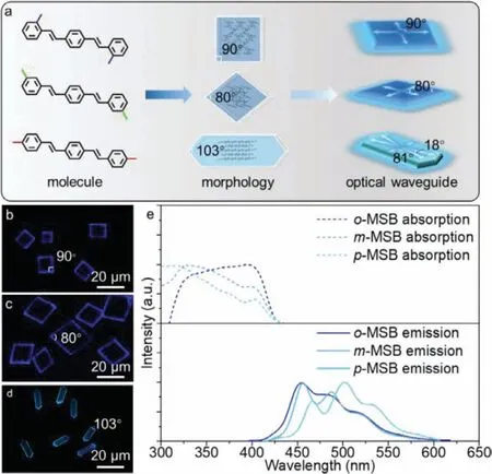
Fig.1.(a) Schematic diagram of three shape-dependent multi-directional 2D optical waveguides with different performances obtained by rational molecular design strategy based on isomer skeleton.Fluorescence microscopy images of (b) o-MSB,(c) m-MSB and (d) p-MSB organic microsheets with a scale bar of 20 μm.(e) Absorption (dashed line) and emission (full line) spectrum of the three microsheets.
It has been demonstrated that the morphology of the crystal can be changed by adjusting the arrangement of molecules,thereby realizing the adjustment of the optical waveguide performance [21].Yaoet al.and his colleagues obtained different selfassembly organic crystals (nanowires and nanosheets) with different optical waveguide performances by adjusting the different dominant intermolecular interactions (H bonding andπ-πstacking) through rational molecular design [22].Notably,sheet-like micro-crystals used for photon conduction medium exhibit unique advantages compared with traditional one-dimensional (1D) crystal materials.These sheet-like crystals usually have polygonal morphology for the reason ofπ-πstacking in two directions between molecules [23],contributes to shape-dependent multi-directional 2D photon conduction within the crystal,which will be more suitable for future chip-level planar photonic integrated systems [24].Furthermore,the control of photon conduction on the micro/nano scaleviachanging the shape of the polygonal microsheets through adjusting the molecular arrangement is crucial for the development of the integrated photonic system.In the previous study,Liet al.prepared two phases of perylene microcrystals by simply controlling the concentration of the solution.Perylene microcrystals with different polygonal shape were obtained because of the different molecular arrangement in these two phases,showing diverse emission colors and 2D optical waveguide performances [25].However,this polymorph strategy is not suitable for all crystals,and there are few reports on universal molecular structure design strategies based on the same molecular skeleton to change the molecule arrangement of sheet-like crystals [26].Therefore,it is still a challenge nowadays to adjust the shape-dependent multidirectional 2D optical waveguide performances of the sheet crystal.
Herein,a molecular design strategy was proposed based on the same isomer molecular skeleton to prepare three different microsheet crystals (Fig.1a).The solid-state packing of the crystals is governed byπ-πstacking in two directions,leading to a 2D molecular arrangement.This 2D molecular arrangement in the three microsheet crystals can be adjusted by only changing the position of the methyl substituents in the isomers,which contributes to different polygonal morphologies of the three microsheet crystals after subtle choice of the crystal growth conditions.Optical tests have demonstrated that the microsheets exhibit three different shape-dependent multi-directional 2D optical waveguide performances,suggesting potential applications in optical devices.
The microsheet crystals of 1,4-bis(2-methylstyryl)benzene(o-MSB),1,4-bis(3-methylstyryl)benzene (m-MSB) (see synthesis method in Supporting information) and 1,4-bis(4-methylstyryl)benzene (p-MSB) are prepared through the mixed solution self-assembly method.Typically,the dichloromethane(DCM) solution (5 mmol/L) ofo-MSB orm-MSB and ethanol were mixed and dropped on the quartz substrate,then covered with a watch glass.After the solvent evaporated,large-scale microsheets can be observed.Due to the poor solubility ofp-MSB in DCM,we chose carbon disulfide (CS2) as the solvent to preparep-MSB microsheet crystals.The CS2solution ofp-MSB is directly dropped onto the quartz substrate,through the remaining same steps,large-scalep-MSB microsheets can be obtained.
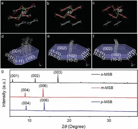
Fig.2.(a–c) The π-π stacking of (a) o-MSB,(b) m-MSB and (c) m-MSB molecules.The red line represents the plane where the molecule is located,and the yellow line represents the π-π stacking between the molecules.The simulated growth morphology of (d) o-MSB,(e) m-MSB and (f) p-MSB based on the attachment energies using the Materials Studio package.(g) The XRD pattern of the as-prepared o-MSB,m-MSB and p-MSB organic microsheets.
The fluorescence microscopy (FM) images of obtained microsheets reveal that these microsheets have different morphologies due to the different positions of methyl substituent.As shown in Figs.1b–d,the shapes ofo-MSB,m-MSB andp-MSB microsheets are rectangle,parallelogram and hexagon,and the Inner angles of them are 90°,80° and 103°,respectively.Meanwhile,the absorption and emission properties of the three crystals are also different,to reveal this difference,the absorption and emission spectra of these three microsheets were tested.Under the excitation of 375 nm ultraviolet light,theo-MSB andm-MSB microsheets show similar blue emission (455 nm),while thep-MSB microsheets show lighter sky-blue emission (500 nm).Besides,as shown in Fig.1e,the maximum absorption wavelengths ofo-MSB andm-MSB microsheets are 400 and 410 nm,respectively.
Through analyzing the single crystal data with Mercury package,the molecular packing of these three crystals were obtained(Figs.2a–c).The existence ofπ-πstacking in two directions between molecules leads to the formation of 2D crystals.Furthermore,we simulated the growth morphology of these three crystals based on the attachment energiesviausing the Materials Studio package (Figs.2d-f).According to the calculated results (Table S2 in Supporting information),the {001}scrystal planes ofo-MSB and the {002}scrystal planes ofm-MSB andp-MSB have the smallest attachment energy (Eatt) among various crystal faces as well as the corresponding highest exposed facet area percentage.In addition,the X-ray diffraction (XRD) measurements of the microcrystals demonstrated these crystal planes are dominant in the crystal (Fig.2g),which makes the microcrystals easy to form sheetlike polygonal structures.The (XRD) measurement ofo-MSB microsheets exhibits a series of intensive characteristic peaks that are from the same sequence of {001}scrystal planes.Likewise,the values ofm-MSB andp-MSB microsheets exhibit a series of intensive characteristic peaks that are from the sequence of {002}s.The actual test results are consistent with the theoretical settlement data.
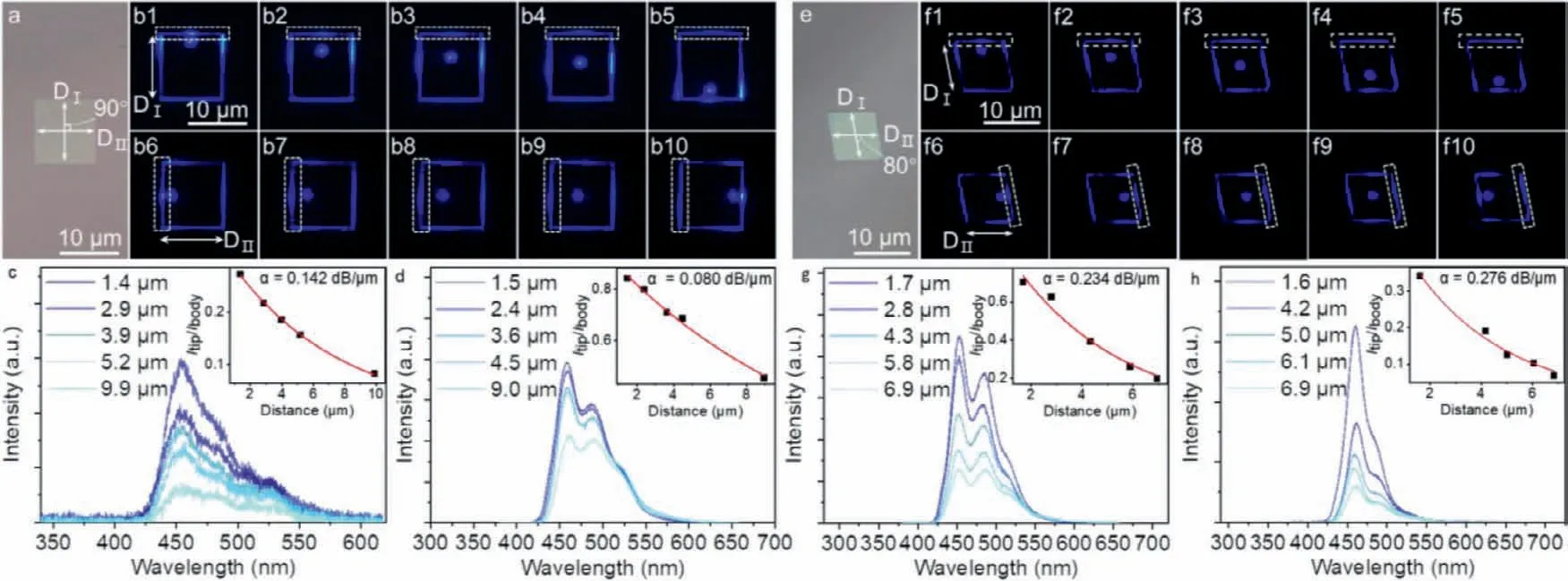
Fig.3.(a) Brightfield micrograph of a typical o-MSB microsheet.(b) Microarea PL images obtained by exciting an identical o-MSB microsheet at different positions in direction I (b1–b5) and direction II (b6–b10).Spatially resolved PL spectra from the edge of the o-MSB microsheet (marked with a dashed frame) for different separation distances between the excitation spot and the edge in (c) direction I and (d) direction II.The inset: nonlinear fitting curve of optical waveguide loss.α: the optical loss coefficient.(e) Brightfield micrograph of a typical m-MSB microsheet.(f) Microarea PL images obtained by exciting an identical m-MSB microsheet at different positions in direction I (f1–f5) and direction II (f6–f10).Spatially resolved PL spectra from the edge of the m-MSB microsheet (marked with a dashed frame) for different separation distances between the excitation spot and the edge in (g) direction I and (h) direction II.
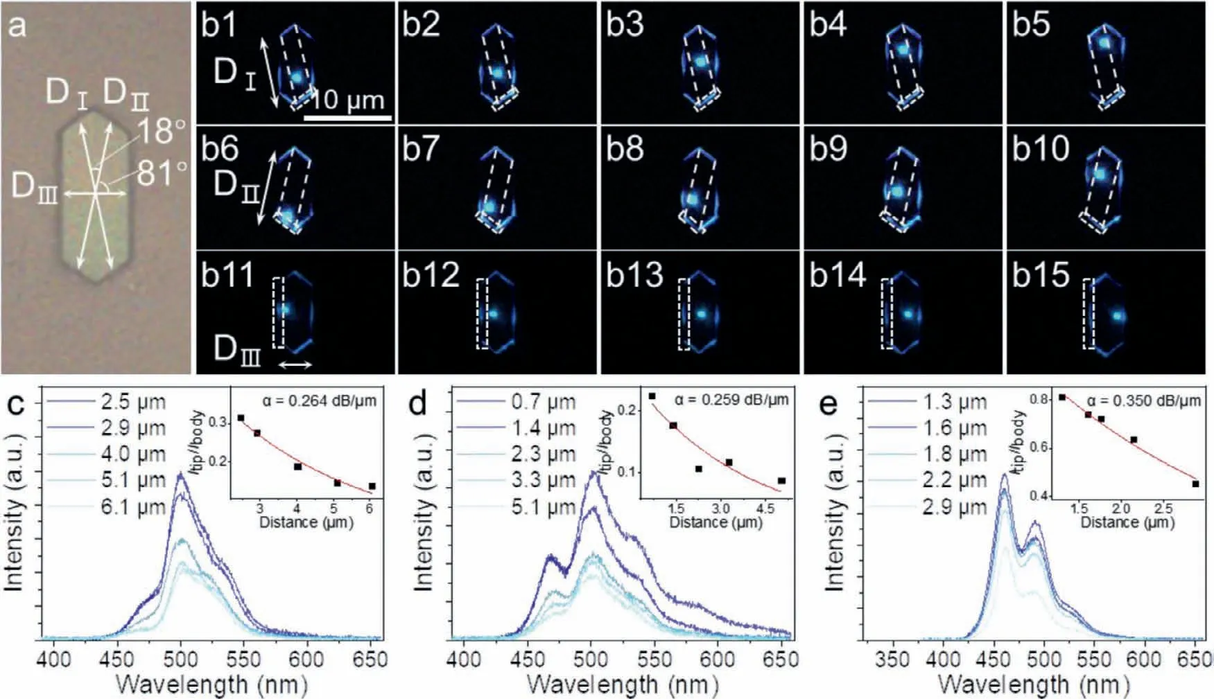
Fig.4.(a) Brightfield micrograph of a typical p-MSB microsheet.(b) Microarea PL images obtained by exciting an identical p-MSB microsheet at different positions in direction I (b1–b5),direction II (b6–b10) and direction III (b11–b15).Spatially resolved PL spectra from the edge of the p-MSB microsheet (marked with a dashed frame) for different separation distances between the excitation spot and the edge in (c) direction I,(d) direction II and (e) direction III.The inset: nonlinear fitting curve of optical waveguide loss.α: the optical loss coefficient.
Importantly,based on the same molecular skeleton of the isomer,the changes in the positions of the methyl substituent leads to the different molecular arrangements in the crystals,which means that the shapes of the three microsheets are different,ultimately reflected in the three different 2D optical waveguide performances.In order to study the different 2D optical waveguide performances of these three crystals,the spatially resolved PL spectra of the microsheets excited by a 375 nm laser were performed (Figs.3 and 4).When the microsheet was excited,the photons propagated in the two-dimensional direction on the microsheet,resulting brighter blue emission at the edges than the middle part of the microsheet surface,which reveals that efficient light guiding can occur within the microsheets.These results demonstrate that the microsheets are excellent optical waveguide materials.Furthermore,it can be found that the optical waveguide performances of the three microsheet crystals are diverse and are related to the shape.Intuitively,o-MSB andm-MSB microsheets are both quadrilaterals with two sets of parallel sides,as a result,the photons propagate mainly in two directions parallel to the sides,and the angles between the two directions are equal to the inner angles of the quadrilaterals.In detail,the photons propagate on theo-MSB microsheets in two mutually perpendicular directions because of the rectangle,shape ofo-MSB microsheets,while them-MSB is a parallelogram with an acute angle of 80°,accordingly,the photons propagate along two directions with an angle of 80° In addition,it can be clearly noticed that the emission intensity at the midpoint of the edge decreases as the propagation length increases.The optical loss coefficients (α) were calculated by a nonlinear fitting equation (y=A1exp(-x/t1)).From the calculation results,the optical loss coefficients in the two directions of a typicalo-MSB microsheet are,respectively,0.142 and 0.080 dB/μm,which are very close,indicating that the crystal structure is uniform.The same test performed onm-MSB revealed that them-MSB microsheet also have similar properties.The optical loss coefficient in direction I (0.234 dB/μm) is almost equal to the value in direction II(0.276 dB/μm) due to the uniformity of the crystal structure.
Different from the bidirectional 2D optical waveguides of theo-MSB andm-MSB microsheets,three-directional 2D optical waveguides is realized based on thep-MSB microsheets because of the hexagonal morphology ofp-MSB microsheets.As shown by the dotted line in Fig.4a,when a typicalp-MSB microsheet was excited by a 375 nm laser,the photons propagated to the edges in three directions.The angles between these three directions have a certain relationship with the internal angle of the hexagon.Through measurement and calculation,the angle between directions,I and II is 18°,and the angles between directions I,III and directions II,III are 81° By changing the position of the excitation point and detecting the edges of the microsheet marked by the dashed frames,the spatially resolved PL spectrum in three directions varied with the propagation length were obtained.Similarly,through calculation,the optical loss coefficients (α) in the three directions are 0.264,0.259 and 0.350 dB/μm,respectively.The small difference in the optical loss coefficients of the three directions indicates thatp-MSB microsheets also have good uniformity of crystal.
In summary,three polygonal microsheet crystals of the three isomer materials were preparedviarational molecular structure design based on the same molecular skeleton.Structural analysis and morphological characterization revealed that the formation of the polygonal shapes of the microsheets is caused by theπ-πstacking in two directions between molecules.The change of the position of the substituents changed the angle ofπ-πstacking and the molecular arrangement on a microscopic level,which further changed the shapes and internal angles of the microsheets on a macroscopic level.In the end,these all manifested in the different photon conduction directions and angles of on the microsheets,which means that the three microsheets achieved different shape-dependent multi-directional 2D optical waveguide performances.This molecular design strategy provides a feasible method for preparing sheet-like crystal materials with adjustable optical waveguide performances as photon transmission medium.
Declaration of competing interest
There are no conflicts to declare.
Acknowledgments
The authors acknowledge financial support from the National Natural Science Foundation of China (Nos.21971185,52173177),and this project is also funded by the Collaborative Innovation center of Suzhou Nano Science and Technology (CIC-Nano),and by the“111′′ Project of the State Administration of Foreign Experts Affairs of China.
Supplementary materials
Supplementary material associated with this article can be found,in the online version,at doi:10.1016/j.cclet.2021.10.076.
 Chinese Chemical Letters2022年6期
- Chinese Chemical Letters的其它文章
- Photochemical defluorinative functionalization of α-polyfluorinated carbonyls via spin-center shift
- Methods of screening,monitoring and management of cardiac toxicity induced by chemotherapeutics
- Light-guided tumor diagnosis and therapeutics: From nanoclusters to polyoxometalates
- Nanofluidics for sub-single cellular studies:Nascent progress,critical technologies,and future perspectives
- Effective purification of oily wastewater using lignocellulosic biomass:A review
- Recent advances in microchip-based methods for the detection of pathogenic bacteria