
Self-gating enhanced carrier transfer in semiconductor electrocatalyst verified in microdevice
2022-07-11 03:39HiynXingYueshoZhengYngChenYntingXuTrvisShihoHuYexinFengYuZhouSongLiuXuliChen
Chinese Chemical Letters 2022年6期
Hiyn Xing,Yuesho Zheng,Yng Chen,Ynting Xu,Trvis Shiho Hu,Yexin Feng,Yu Zhou,Song Liu,∗,Xuli Chen
a State Key Laboratory of Chemo/Biosensing and Chemometrics,College of Chemistry and Chemical Engineering,Hunan University,Changsha 410082,China
b Hunan Provincial Key Laboratory of Low-Dimensional Structural Physics and Devices,School of Physics and Electronics,Hunan University,Changsha 410082,China
c Department of Mechanical Engineering,California State University,Los Angeles,CA 90032,United States
d School of Physics and Electronics,Central South University,Changsha 410082,China
e College of Materials Science and Engineering,Hunan University,Changsha 410082,China
Keywords:Chemical vapor deposition Pt NPs@MoS2 Hydrogen evolution reaction Microelectrochemical Self-gating
ABSTRACT Semiconductor electrocatalysis with weak conductivity can accumulate extremely high carriers at semiconductor-electrolyte interface by self-gating effect,which strongly promotes electrocatalytic effi-ciency.The correlation between semiconductor carrier mobility and electrocatalysis performance is still unclear.Herein atomic-thin transition metal dichalcogenides based composites have been developed for hydrogen evolution reaction (HER) performed with on-chip microdevices.Electrical and electrochemical measurement of individual flack verified the key role of high carrier mobility for enhanced HER activity.Carrier mobility regulation further demonstrated its high dependence with HER performance under self-gating.Our study provides new insight into the carrier mobility of the semiconductor in the electrocatalysis,paving the way for designing high-performance semiconductor catalysts.
Hydrogen is an ideal candidate of clean and sustainable energy carrier,attributed to its high energy density and environmentalfriendliness during storage,delivery and usage [1,2].Watersplittingviahydrogen evolution reaction (HER) is an essential hydrogen production strategy,in which renewable and highly effi-cient electrocatalysis is urgently needed to reduce thermodynamic barrier and improve energy conversion [3,4].So far,Platinum (Pt)has been demonstrated to exhibit the excellent thermoneutral adsorption energy of hydrogen intermediates (e.g.,H3O+),thus ensuring the fast kinetics towards HER.Recently,transition metal dichalcogenides (TMDs),as a kind of earth-abundant materials with extraordinary physical and chemical properties,have emerged as potential alternative to the precious Pt-based catalysis [5–7].Tremendous research efforts in various forms have been devoted to optimize HER performance,e.g.,improving active site in the basal plane [8],doping heteroatoms into the lattice [9–13],phase or strain engineering and interface electronic coupling [14].
In contrast,less attention has been paid to the role of carrier mobility,the important parameter for semiconductor,due to technical limit and difficulty to trace one single factor.Traditional electrocatalysis has complicated transfer steps and ambiguous active area,making it difficult to study the underlying mechanisms [15,16].Microcell fabrication for electrocatalytic test has drawn extensive interests which can accurately measure novel 2D materials with special reactive sites [17–19].Typical examples include 2H or 1T phases [20],explicit contrast of basal plane with edge [21,22],heterojunction and anisotropic structures [23,24],definite boundary [25],and all of which [26–32]have provided more insightful information on the correlation between microstructure and electrochemical performance.In addition,the novel microcell-based measurement strategy enabled the exploration of the semiconductor-electrolyte interfaces,which can strongly modulate the surface conductance of semiconductor electrocatalyst during “self-gating” [15].The demonstration of selfgating can improve our understanding of various semiconductorelectrolyte interfaces in the field of electrochemistry,and leave enormous room to explore semiconductor properties and electrocatalytic performance [14,33,34].Typically,carrier mobility is the intrinsic property for semiconductor,which can be defined as charge confine in the 2D lattice plane and responsible for the variation of the physicochemical properties in the field gating.Regulation of the electronic structure of semiconductor catalysis is the usual approach to enrich the electrocatalysis activities.Because of the self-gating action,evaluating the role of carrier mobility during electrocatalysis is of great importance.However,the exact function of single-domain for carrier mobility to influence the HER performance is hardly defined for various TMDs with different atoms.
Herein,we propose a facile chemical vapor deposition (CVD)method to enhance the carrier mobility by simultaneously growing non-planar Pt NPs@MoS2nanocomposites.Experimental results reveal that early reductive Pt NPs lead to the ripple morphology of MoS2films,which possess unconventional triangle and hexagonal morphology.Besides,Pt NPs and MoS2are weakly combined,which have been verified by X-ray photoelectron spectroscopy (XPS).Microcell-based electrical and electrochemical tests offer unique platform to acquire the correlation between the carrier mobility and electrocatalytic performance.Further carrier mobility regulation for Pt NPs@MoS2with different molar ratios demonstrate that effective charge transfer under the self-gating is strongly correlated with the HER performance.High carrier mobility of Pt NPs@MoS2(3.0± 0.3 cm2V−1s−1) corresponds to high HER performance (−0.063 V,72.4 mV/dec).
CVD growth of MoS2,Pt NPs-MoS2and Au NPs-MoS2: An atmospheric pressure furnace was used for CVD growth of MoS2,Pt NPs@MoS2and Au NPs@MoS2.Based on our previous work,the precursor,0.01 mol/L sodium molybdate (Na2MoO4,99%,Aladdin),was obtained by dissolving 20.6 mg Na2MoO4in 10 mL of deionized water.The precursor of Pt NPs@MoS2was acquired by mixing 995 μL of 10 mmol Na2MoO4with 5 μL of 24.4 mmol H2PtCl6.Au NPs@MoS2was obtained by mixing 995 uL of 10 mmol Na2MoO4with 5 μL of HAuCl4.(20 mmol/L).The fresh SiO2/Si wafer was treated by 60 W of oxygen plasma for 30 s (CIF Tech Co.,Ltd.CPCC-40 KHz).Different precursor solutions were spin-coated on the treated wafer at 3000 rpm for 1 min.The SiO2/Si wafer with precursor was loaded into the center of the furnace.Crucible with 150 mg ofSpowder (China Sinopharm Co.,Ltd.) was located 13 cm upstream the heating belt.Argon was used as carrying gas at a flow rate of 270 sccm and the growth temperature was gradually raised to 850 °C in 40 min,and subsequently kept for 4 min at the set point after pushing S powder into the hot zone.Different growth temperatures and time were applied following the above procedure.
The morphology of samples was characterized by optical microscopy (Nikon H600L),SEM (Hitachi-S4800),EDS (Horiba 7021-H),and AFM (Bruker Dimension Icon AFM).Raman,PL and mapping spectroscopy were collected by WITec Alpha 300R spectrometer using a 532 nm laser excitation.The X-ray diffraction (XRD) of sample was performed by Bruker Dimension Icon D8 advance using Cu-Kαradiation (40 kV,40 mA).The valence state and surface composition were examined by XPS (Escalab 250Xi).The electrical properties of the device were tested on Lakeshore probe station(EPS150COAX) by Keithley Sourcemeter 2634B at room temperature under ambient conditions.STEM images were obtained by using a JEOL 2100F microscope equipped with a cold field-emission gun and double dodecaple correctors operating at 60 kV.The probe current was at ∼25−30 pA.
After CVD growth,SiO2/Si wafer with product was spin-coated with SPR-220–3a photoresist at 4000 rpm for 60 s and baked at 115 °C for 90 s.Subsequently,the prepared SiO2/Si wafer was patterned by ultraviolet and deposited with In/Au (10 nm/50 nm) by thermal evaporation to connect the square pad and the nanosheet.Residual photoresist was removed by acetone following a lift-off process,and the final metallic electrode wafer was obtained.Furthermore,in the micro-electrocatalytic process,a layer of photoresist was spin-coated on the SiO2/Si wafer,with evaporated metallic electrode,and exposed under proper ultraviolet beam to open a window on the target position of nanosheet.The residual photoresist help to protect the device and avoid unfavorable effect from the Au electrode and another nanosheet.
The performance of micro-electrocatalysis was tested by a three-electrode system using a CHI 660E electrochemical workstation.The exposed area of the nanosheet served as the working electrode,a Pt filament with a diameter of 0.6 mm served as the count electrode,and self-made saturate Ag/AgCl electrode served as reference electrode.The HER activity of polarization curve was evaluated in the electrolyte of 0.5 mol/L H2SO4by LSV at a scan rate of 5 mV/s.All reported potentials were converted to RHE potentials.
All the theoretical simulations were carried out using the DFT method implemented in the Viennaab-initiosimulation package(VASP) [40,41].The exchange correlation energy was described by the generalized gradient approximation (GGA) in Perdew-Burke-Ernzerhof (PBE) form [42].Atomic positions and lattice constants of all structures were relaxed until the forces acting on the atoms were less than 0.01 eV/ ˚A.A 6× 6× 1 supercell of monolayer MoS2was constructed,which contains 108 atoms with a vacuum area of 15 ˚A.To simulate the MoS2edge,6× 6× 1 rectangular nanoribbon structure was employed,and the nanoribbon was sufficiently separated with a vacuum space of ∼15 ˚A.The plane-wave cutoff energy was set to 400 eV,and theΓ-centered Monkhorst-Pack method with the k-meshes of 2× 2× 1 and 2× 1× 1 were used.
The Gibbs free energy was calculated according to the formulaΔG=ΔE+ΔZPE-TΔS,where theΔEwas the hydrogen adsorption energy,ΔZPE was the zero-point energy correction,andΔSdenoted the difference between the adsorbed state and the gas phase in entropy,respectively.During electrochemical reaction,the reaction energy of (H++e-) in solution was estimated as the energy of 1/2 H2.In this work,ΔZPEandTΔSwere 0.06 eV and−0.18 eV for all considered cases,yieldingΔG=ΔE+0.24 eV
Proper precursor solutions with different molar concentrations of Na2MoO4have been investigated.Higher molar ratio of Na2MoO4and longer growth time generally result in thick materials while the crack of formed structure appeares in 10 min(Fig.S1 in Supporting information).Figs.1a–d illustrate the CVD process to obtain atomic-thin Pt NPs@MoS2.Beyond previously reported wafer-scale growth of MoS2,H2PtCl6solution is added to simultaneously form Pt NPs thus realizing the co-growth of Pt NPs and MoS2[35].Some small triangular materials are deposited on the atomic-thin film.Fig.S2 (Supporting information)shows the atomic force microscope (AFM) topography image of Pt NPs@MoS2,indicating that the thickness is 0.94 nm.The obtained Pt NPs@MoS2and monolayer MoS2are examined by Raman spectroscopy (Fig.1e).Typical vibration signals of E12gand A1gare presented,which represent the in-plane and out-of-plane vibration of atoms,respectively.A red-shift of the A1gpeak of Pt NPs@MoS2is shown in comparison with the monolayer MoS2.The frequency difference (Δk) is 22.5 and 20.6 cm−1,respectively,consistent with the widely accepted bilayer and monolayer MoS2films as reported in previous work [36].Meanwhile,we carry out photoluminescence (PL) measurement (Fig.1f).The characteristic MoS2PL emission peaks of exaction A and B are centered at around 1.8 eV and 2.0 eV,respectively (Fig.S3 in Supporting information).The decreased PL intensity and red-shift of Pt NPs@MoS2imply the quenching of PL between adjacent layers.Corresponding integrated intensity mapping of Raman spectra (A1g,403 cm−1) and a PL peak(1.78 eV) are presented in Figs.1g and h,which show the nonuniformity of Pt NPs@MoS2surface.The Raman,PL and thickness tests agree well with the results from above optical image (OM).Some small triangular materials are deposited on the monolayer film.The Pt atoms introduced during the CVD led to large difference of morphology comparing with traditional MoS2with triangle and hexagonal edge [37].To analyze the growth mechanism,the product growing at 650 °C is assessed by a combination of optical microscope and XPS (Fig.S4 in Supporting information).Comparing with unreacted precursor in Fig.S5 (Supporting information),small nanoparticles emerge (Fig.S6 in Supporting information),consist of typical Mo(VI),Pt(0) and a small amount of Pt(II),revealing the emergence of nucleation in MoS2,Pt NPs and intermediate Pt.
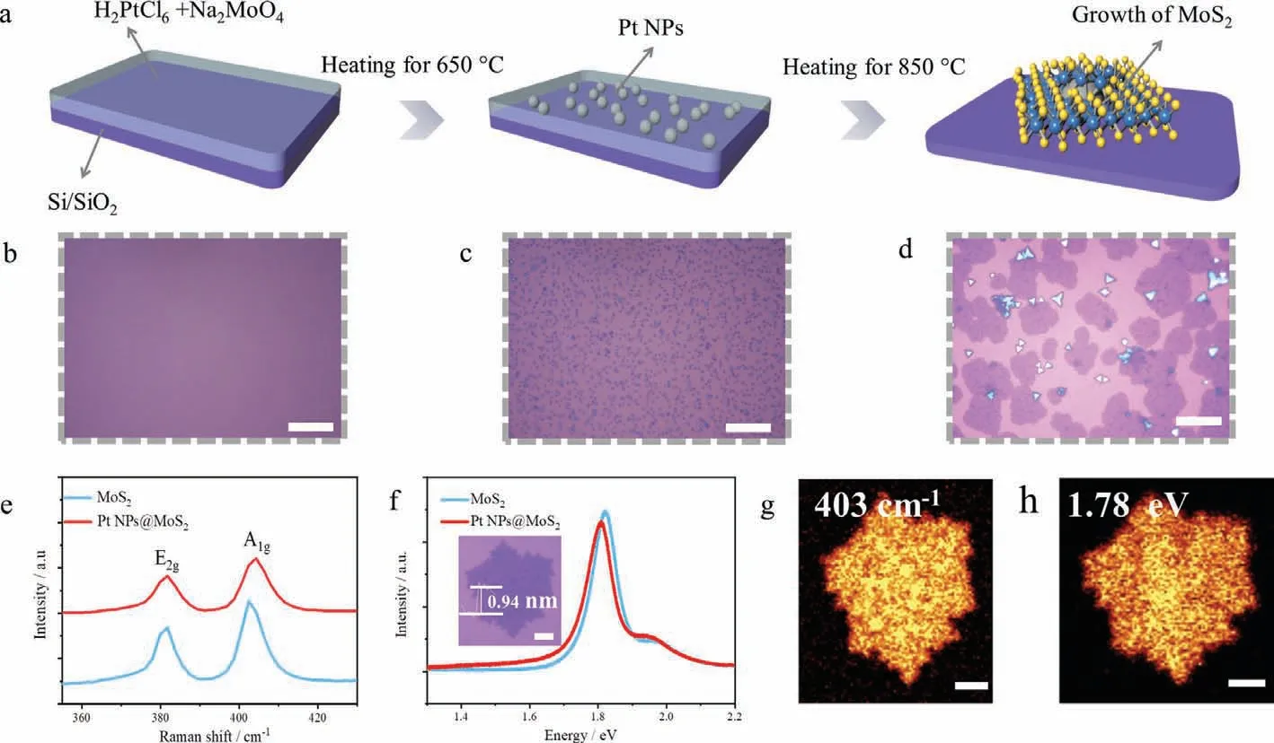
Fig.1.(a) Schematic of co-growth process of Pt NPs@MoS2.Optical images corresponding to (b) precursor-solution of H2PtCl6+Na2MoO4.(c) Pt NPs for the first reduction in the growth process.(d) Final Pt NPs@MoS2 products (Scale bar: 20 μm).(e) Raman and (f) PL spectra collected from Pt NPs@MoS2 and MoS2. Inset: optical image of Pt NPs@MoS2 (Scale bar: 3 μm).Intensity mapping of (g) Raman at 403 cm−1 and (h) PL at 1.78 eV for Pt NPs@MoS2 (Scale bar: 3 μm).
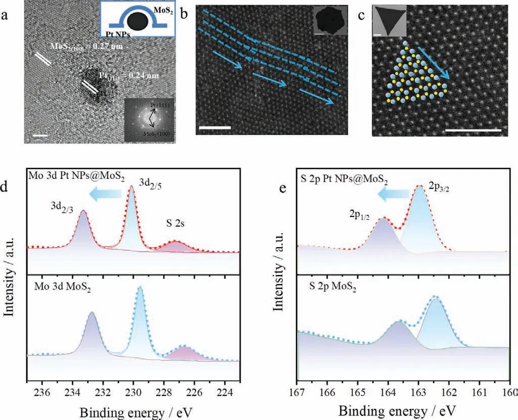
Fig.2.(a) HRTEM image of Pt NPs@MoS2 showing typical lattice spacing of MoS2(100) and Pt (111) (Scale bar: 2 nm).Inset: FFT of two sets of diffraction spots,corresponding to MoS2 and Pt.(b) HAADF STEM investigation of Pt NPs@MoS2,the region marked in blue dashed line showing the non-liner growth direction of Pt NPs@MoS2 (Scale bar: 2 nm).Inset: SEM of Pt NPs@MoS2 (Scale bar: 10 μm).(c)HAADF STEM image of MoS2 showing typical triangular morphology (Scale bar:2 nm).Inset: SEM of MoS2 (Scale bar: 5 μm).XPS spectra showing Mo 3d (d) and S 2p (e) of Pt NPs@MoS2 and MoS2.
To elucidate the microstructure of such Pt NPs@MoS2,TEM is adopted.HRTEM and the corresponding Fourier transform (FFT) of the Pt NPs decorated MoS2are shown in Fig.2a.The lattice fringes of 0.27 nm and 0.24 nm represent the MoS2(100) and Pt (111),respectively.The X-ray diffraction (XRD) of Pt NPs@MoS2has been shown in Fig.S7 (Supporting information),typical (002) peak of MoS2is shown at 14° implying the same lattice structure of such two materials.X-ray spectrometers (EDX) element analysis (Fig.S8d in Supporting information) is implemented to further verify the composition of the nanocrystals.Ripple morphology exists in the MoS2,and a set of diffraction spots imply the single-direction crystal growth.Besides,the region of MoS2film without Pt NPs also shows ripple stripes and single-direction growth (Fig.S8b in Supporting information).It is illustrated that ripple morphology exists not just surrounding Pt NPs but also spreading out,leading to irregular morphology.From the enlarged image of Pt NP in Fig.S8a (Supporting information),the lattice spacing of MoS2and Pt co-exists in the space of Pt NP,which implies the growth of MoS2film over the small Pt NP instead of surrounding it.In addition,STEM is conducted as shown in Fig.2b.Analysis of the atomic structure reveals nonlinear atomic growth direction.Such transformation of stripe growth results in unusual morphology of hexagonal or triangle MoS2.Fig.2c shows the atomic structure of film MoS2with linear edge,which is drastically different from that of Pt NPs@MoS2.The morphological change is attributable to a compressive force exerted by Pt atom in the growth process.XPS spectra of MoS2and Pt NPs@MoS2have been shown in Figs.2d and e and Fig.S9 (Supporting information),respectively.Typical peaks of Mo (3d5/2and 3d3/2) appear in the two spectra,along with distinctive shift of high binding energy in the Pt NPs@MoS2,where the two peaks center at 230.1 eV and 233.3 eV compared to pure MoS2(229.5 eV and 232.7 eV).The S 2p spectrum shown in Fig.2d agrees well with the shift of Mo 3d,suggesting the weak combination between Pt NPs and MoS2.Pt 4f spectra of Pt NPs@MoS2with low and high Pt concentrations are shown in Fig.S10 (Supporting information).Pt NPs@MoS2with low Pt content show ambiguous peak.However,stronger Pt(0) peaks in 71.8 eV and 75.2 eV is attributed to higher concentration of Pt,indicating that the Pt is mainly in the form of NPs.
Qualitative analysis of the Pt NPs@MoS2growth mechanism has been demonstrated.The CVD precursor is a mixture of Na2MoO4and H2PtCl6.As the growth of Pt NPs@MoS2proceeds,the PtCl62−is firstly reduced thus forming small nanoparticles under low thermodynamic condition.MoS2film growth begins when the melting temperature of Na2MoO4achieves at 687 °C [36].Small Pt NPs can facilitate further nucleation of MoS2at the initial stage.Subsequently,with the rising temperature,vaporized sulfur dissolves into the liquid,thus triggering the formation of MoS2.Continuous precipitation allows MoS2film to grow,once it encounters the Pt NPs at the growth front,the film tends to grow over the particles,leading to the unusual ripple stripes of MoS2.It agrees with the observed distorted morphology and nonlinear atomic alignment.The Pt NPs serve as the nucleation sites and assist the growth of irregular structure of MoS2.Notably,these small nanoparticles can easily induce the growth of second layer in the tested system [25].The XPS result shows the weak shift of binding energy of Mo and S,which implies the weak binding of Pt NPs with the MoS2film.
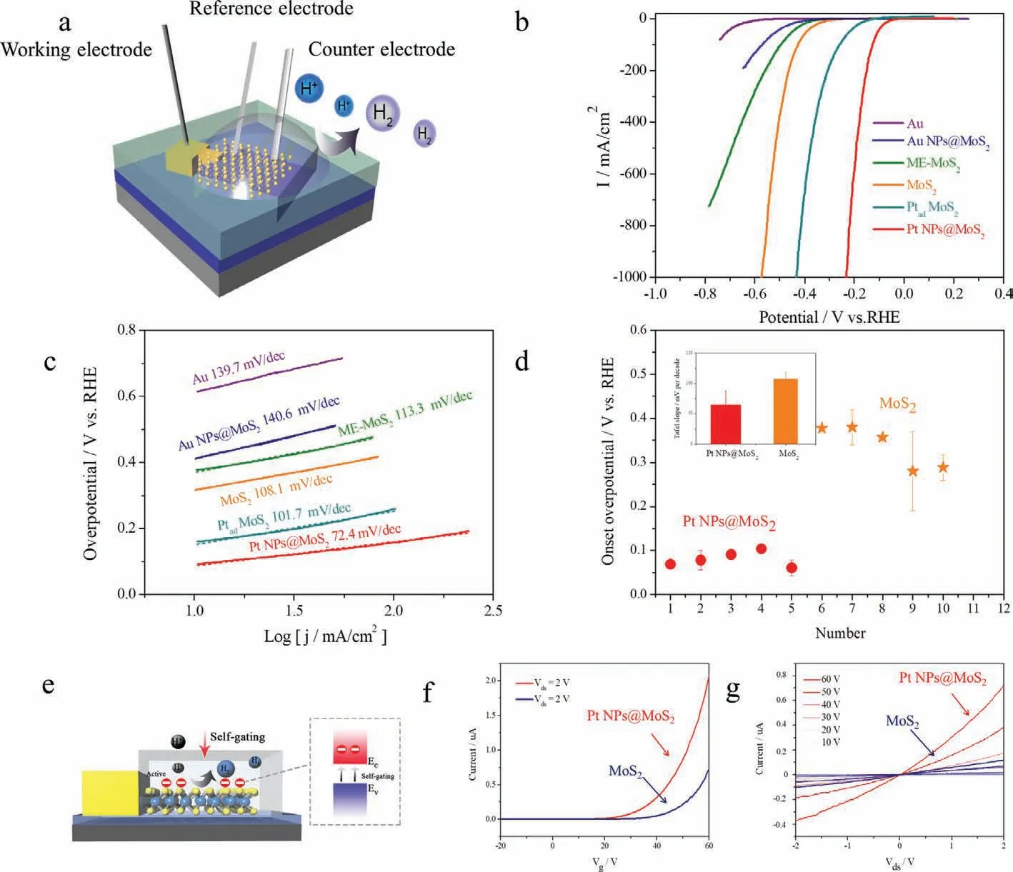
Fig.3.(a) Schematic of the electrochemical microcell setup for the HER.(b) LSV curves for the Au,Au NPs@MoS2,ME-MoS2,MoS2,Ptad−MoS2,Pt NPs@MoS2.(c) Corresponding Tafel slope of the LSV curves in (b).(d) The statistics of onset overpotential of MoS2 and Pt NPs@MoS2 from different devices.Inset: statistical Tafel slopes of MoS2 and Pt NPs@MoS2.(e) The self-gating turns on and facilitates the transfer electron on the surface of semiconductor under HER.(f) Transfer curves (Ids-Vg) of MoS2 and Pt NPs@MoS2 with Vg from −20 V to 60 V at Vds=2 V.(g) Output curves (Ids-Vds) of MoS2 and Pt NPs@MoS2 measured at different Vg from 10 V to 60 V with a step of 10 V.
Aimed at precisely acquiring the HER performance of target location,we construct microcell devices by photolithography technique for electrochemical test,which can open the window of desired position during the development (Fig.S11 in Supporting information).As shown in Fig.3a,a drop of 0.5 mol/L H2SO4is placed on the micro-window,a Pt wire and Ag/AgCl serve as counter and pseudo-reference electrodes (Fig.S12 in Supporting information),respectively.Au,mechanical exfoliated MoS2,CVD MoS2are tested to verify the reliability of the micro-electrocatalytic system(Figs.3b and c).The onset overpotentials are −0.614 V,−0.377 V and −0.317 V at 10 mA/cm2(versusRHE),and the Tafel slopes of these materials are 139.7 mV/dec,113.3 mV/dec and 108.1 mV/dec,respectively.The HER performance of the above materials relies on micro-electrocatalysis,which is consistent with previous report [20].Typically,Pt NPs@MoS2shows remarkable HER performance with onset overpotential of −0.0627 V and Tafel slope of 72.4 mV/dec.The OM,Raman and PL of Au NPs@MoS2,which is prepared using the same method (substituting H2PtCl6with HAuCl4as the precursor),have been characterized in Fig.S3.The HER performance becomes poor (−0.412 V,140.6 mV/dec).In order to verify the superior performance of Pt NPs@MoS2,we directly add Pt NPs dispersion in monolayer MoS2,and the tested performance are −0.160 V and 101.7 mV/dec.To further test the reliability of HER properties,we measure multiple devices and the corresponding data are shown in Fig.S13,Tables S1 and S2 (Supporting information).From Fig.3d,in general,Pt NPs@MoS2has the best HER properties (average overpotential is around 0.08± 0.017 V),and the next is MoS2(0.34± 0.048 V).Similar tendency appears in the Tafel slope,Pt NPs-MoS2presents the lowest slope of 64.7±22.4 mV/dec,smaller than that of MoS2(106.8± 11.3 mV/dec).TheΔGH∗ of Pt NPs@MoS2also have been simulated,we adsorb Pt clusters with different atom numbers on the monolayer MoS2.After DFT optimization,we obtain the most stable chemisorption models of the H atom on different system surfaces,as shown in Fig.4a.Pt introduction can increase the active site and decrease the adsorption free energy H∗(ΔGH∗),which has been verified in Fig.4b.The catalytic activity of intrinsic MoS2and Pt NPs@MoS2systems in the HER has been studied theoretically using the density functional theory (DFT) method.TheΔGH∗is an important indicator of the HER activity,where moderateΔGH∗facilitates both feasible H adsorption and satisfactory H2desorption.As shown in Fig.4b,the calculatedΔGH∗of PtXad(X=3,4,13) is much closer to zero thn that of MoS2(both basal plane and edge site),indicating that Pt NPs@MoS2in the co-growth system is more active than the pure MoS2for HER activity,attributed to favorableΔGH∗.
Engineering the electronic state is an inherent method to enhance the performance of catalysis,which mainly depends on two factors of extra electron injection and transfer.Corresponding electrical transport properties can be acquired by micro-device fabricated in a physical property measurement system.Therefore,in order to obtain more information on the performance and conductivity of Pt NPs@MoS2,back-gated field-effect transistors (FETs) are fabricated on the 285 nm SiO2/Si substrates to evaluate the electrical properties of Pt NPs@MoS2.The devices are preparedviathe photolithography and then thermally evaporated with 10/50 nm In/Au (Fig.S14 in Supporting information).TheId/Vdcurves at different gate voltages have been tested (Fig.3g).Linear and symmetric curves suggest the Ohmic-like contact at the metallic electrode and Pt NPs@MoS2,consistent with past report on contract between In and MoS2[38].It means charge can effectively transfer across the interface between the metallic In and Pt NPs@MoS.Furthermore,the current signal is enhanced in Pt NPs@MoS2compared to MoS2.Fig.3f shows the transport characteristics ofId/Vg,indicating the typical n-type conduction and current signals of Pt NPs@MoS2and MoS2.Similar to the MoS2FETs,positive electric field facilitates the electron transfer.In order to further verify the conductivity,five channels of each Pt NPs@MoS2and MoS2are measured (as listed in Table S3 in Supporting information).Remarkably high carrier mobility of Pt NPs@MoS2(3.0± 0.3 cm2V−1s−1) is recorded,which is 5.89 times than that of MoS2(0.5 5± 0.1 cm2V−1s−1).Thus,the introduction of Pt greatly improves the transfer property of MoS2,resulted from the weak interaction between Pt NPs and MoS2.The ripple morphology of Pt NPs@MoS2also serves an important role,which has been verified in the past study [39].Furthermore,the carrier mobility of Pt NPs@MoS2is apparently higher than that of MoS2,leading to lower Tafel slope and faster charge transfer.Density of states (DOS) calculation is performed in Fig.4c.After decorating the Pt clusters into MoS2(Pt3ad),the DOS near the top of the valence band and the bottom of the conduction band are increased,indicating that more charge carriers are involved in the catalytic reaction,significantly improving the HER performance.The self-gating phenomenon in Fig.3e can explain the high efficiency of Pt NPs@MoS2as electrocatalysts comparing with that of MoS2,although semiconductor has always been identified as non-ideal catalysis due to their low intrinsic conductivity.The selfgating can induce a charge transport pathway that renders the surface of ultrathin semiconductors to be highly conductive.When the semiconductor catalyst is turned on under self-gating,its surface becomes conductive and cathodic/anodic reaction takes place.The surface conductivity of a semiconductor catalyst is strongly correlated with their electrocatalytic activity.As a result,n-type ultrathin semiconductor of Pt NPs-MoS2and MoS2catalysts can be turned on by negative electrochemical potential (positive gating),and a remarkable HER performance of Pt NPs@MoS2relies on its high carrier mobility in the electrocatalysis in above discussed circumstance [15].
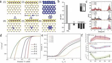
Fig.4.(a) Chemisorption models of the H atom on the (1) basal plane,(2) S-edge of the MoS2,(3) Pt {111} surface,only two layers are displayed,(4) Pt3ad surface,(5) Pt4ad surface and (6) Pt13ad surface.(b) Free energy diagram for the HER on PtXad (X=3,4,13),Pt {111} surface,and pure MoS2 (S-edge and basal plane).(c) Calculated total and projected DOS of pure MoS2 and Pt3ad.(d) LSV curves for the P-1,P-2,P-3,P-4 and P-5.(e) Transfer curves (Ids-Vg) of P-1,P-2,P-3,P-4 and P-5.(f) The statistical data of Tafel slope,onset overpotential and carrier mobility for the P-1,P-2,P-3,P-4 and P-5.
To better trace the influence of carrier mobility in the electrocatalysis process.The precursors with different molar ratios of H2PtCl6have been explored and corresponding morphology is shown in Fig.S15 (Supporting information).Transport characteristics ofId/Vgfor different molar ratios of Pt NPs@MoS2have been tested (Fig.4e).P-1 displays the best conductance with the increase of positive gate,the poor conductance is presented by P-2 and P-3.To check the reliability of the trend,we have tested several devices and the statistical results are listed in Table S4 (Supporting information),similar to the trend shown in Fig.4f.Besides,the linear plot ofId/Vdcurves at different gate voltages have been tested,as shown in Fig.S16 (Supporting information),revealing the Ohmic-like contact of electron injection between Pt NPs@MoS2and In/Au pad.However,the PL and Raman spectra for the different molar ratios of Pt NPs@MoS2display almost unchanged peak position (Fig.S17 in Supporting information).The reason for the change may be that P-2 and P-3 shows damaged crystal with the increase of Pt NPs.When the size of Pt NPs is further increased,P-4 and P-5 become smaller with slightly damaged crystal,as shown in Figs.S18 and S19 (Supporting information).The integrity of the crystal to a large extent will influence the carrier mobility of nanosheet,e.g.,P-1,P-4 and P-5 with better crystal show higher carrier mobility.Next,the linear polarization curves of P-1,P-2,P-3,P-4 and P-5 have been measured (Fig.4d and Fig.S20 in Supporting information).Notably,P-1 shows the best onset overpotential among the different Pt NPs@MoS2with −0.063 V,P-2 and P-3 show relatively poor values of −0.296 V and −0.243 V.The HER performance of P-4 and P-5 is increased,showing −0.1361 V and −0.1198 Vvs.reversible hydrogen electrode (RHE),respectively.The Tafel profiles are demonstrated in Fig.S21 (Supporting information),showing the same trend for the onset overpotential.P-1 presents the lowest slope of 72.4 mV/dec and the next ones are P-4 and P-5 (130.5 and 109.4 mV/dec),the last ones are P-2 and P-3 (144.9 and 143.2 mV/dec).In order to acquire reliable data,we have fabricated five devices and collected the onset overpotential and Tafel slope (Table S6 in Supporting information).In Fig.4f,the HER performance displays strong correlation with the carrier mobility,i.e.,higher carrier mobility will lead to lower onset overpotential and Tafel slope.
TheΔGH∗of Pt NPs@MoS2with different concentrations of Pt also have been simulated,we adsorb Pt clusters with different atom numbers on the monolayer MoS2.After DFT optimization,we obtain the most stable chemisorption models of the H atom on different system surfaces,as shown in Fig.4a.In Fig.4b,the calculatedΔGH∗ of PtXad(X=3,4,13) is much closer to zero.The catalytic performance of Pt NPs@MoS2co-growth system remains mostly unchanged with the increase of Pt cluster,which is slightly different from the experimental results.From above discussion,the carrier mobility of semiconductor can greatly influence the HER performance.In view of the tested film is ultrathin,the self-gating phenomenon,which could induce a charge transport pathway and high conductivity in semiconductor,take places in the HER reactions,suggesting that electrocatalytic activity is strongly dependent on the transistor behavior of semiconductor [15].As discussed above,high mobility and conductivity of Pt NPs@MoS2enables higher HER activity (lower onset potential and Tafel slope) compared with MoS2.High carrier concentration could be a contributor to facilitate charge transfer in the inherently inert semiconductor.The experiment on different molar ratios of Pt NPs@MoS2further proves the key role of carrier mobility.AlthoughΔGH∗ values for P-2,P-3,P-4 and P-5 are almost similar,under self-gating,poor charge transfer of P-2,P-3 still lead to relatively low HER activity.
In summary,we have successfully synthesized Pt NPs@MoS2with unusual triangle or hexagonal morphology through CVDbased co-growth,exhibiting enhanced carrier mobility.Microdevice is fabricated as a proof of concept for directly evaluating the HER performance.Transport test and theoretical studies indicate that theΔGH∗is decreased with the increased active sites and improved carrier mobility of Pt NPs@MoS2.It contributes to a significantly improved catalytic activity and efficient charge transfer for enhancing HER compared with MoS2.Furthermore,benefiting from the regulation of carrier mobility (viasynthesizing different molar ratios of Pt NPs@MoS2),the variation tendency of efficient charge transfer of semiconductor under self-gating demonstrates strong correlation with the HER performance.The methodology presented here demonstrates the importance of the carrier mobility in engineering the performance of catalysis,and can promote further efforts on exploring efficient catalysis.
Declaration of competing interest
The authors declare that they have no known competing financial interests or personal relationships that could have appeared to influence the work reported in this paper.
Acknowledgments
S.Liu acknowledges the National Natural Science Foundation of China (No.22175060,21975067).Y.Feng acknowledges the National Basic Research Programs of China (No.2016YFA0300901) and the National Science Foundation of China (No.11974105).T.S.Hu acknowledges the support from the U.S.National Science Foundation CREST Program (NSF No.HRD-1547723).Y.Zhou acknowledges the National Natural Science Foundation of China (No.51902346).X.Chen acknowledges Natural Science Foundation of China (No.21805077) and the Natural Science Foundation of Hunan Province(No.2019JJ50075).
Supplementary materials
Supplementary material associated with this article can be found,in the online version,at doi:10.1016/j.cclet.2021.10.033.
 Chinese Chemical Letters2022年6期
- Chinese Chemical Letters的其它文章
- Photochemical defluorinative functionalization of α-polyfluorinated carbonyls via spin-center shift
- Methods of screening,monitoring and management of cardiac toxicity induced by chemotherapeutics
- Light-guided tumor diagnosis and therapeutics: From nanoclusters to polyoxometalates
- Nanofluidics for sub-single cellular studies:Nascent progress,critical technologies,and future perspectives
- Effective purification of oily wastewater using lignocellulosic biomass:A review
- Recent advances in microchip-based methods for the detection of pathogenic bacteria