Machine Learning Produces Superhuman Chip Designs
Robert Pollie
Senior Technology Writer
First it was chess,then it was Go.Now artificial intelligence(AI)is challenging human supremacy in a far more complex—and commercially significant—undertaking: designing microchips. In June 2021,researchers at Google Brain(Google’s deep learning division)reported that they had devised a machine learning system that can produce manufacturable chip floorplans in a small fraction of the time taken by human experts.Writing in the June 10 online edition of Nature [1], a Google team headed by research scientists Azalia Mirhoseini and Anna Goldie stated that ‘‘in under 6 hours, our method automatically generates chip floorplans that are superior or comparable to those produced by humans in all key metrics,including power consumption, performance, and chip area.”
While other companies, including Cadence, International Business Machines (IBM), and Nvidia, have implemented their own machine learning-based chip design solutions [2,3], Google’s is apparently the first to surpass humans at floorplanning.The feat is an important milestone for AI and may significantly shorten the development of new microprocessors and other advanced chips.The editors of Nature hailed the result as ‘‘an important achievement that will be a help in speeding up the supply chain” [4]. In fact,Google is already putting the system to work,using it to craft floorplans for the company’s next-generation AI accelerator chips.
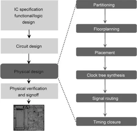
Floorplanning is an early stage in the physical design of microchips (Fig. 1). It consists of arranging large blocks (i.e., macros) of memory and logic control in a rectangular area representing the chip surface. After an initial floorplan is sketched out, smaller chunks of logic (i.e., standard cells) are placed in the remaining open spaces,and wires are routed to connect the macros and cells[5].
Floorplanning is a delicate balancing act,in which designers try to simultaneously minimize the chip area, keep wire lengths as short as possible, avoid routing congestion, and meet timing requirements and other design criteria. The overall goal is to achieve an optimal combination of chip performance, power consumption, and cost [6].
It is a dauntingly complex task. Today’s larger chips may have hundreds or thousands of macros and millions or billions of standard cells, connected by kilometers of wiring. The number of possible floorplan arrangements is astronomical. For example, the floorplans in the Google study have more than 102500possible configurations, according to Mirhoseini et al. [1]. By comparison,the game of Go has 10360. The combinatorial complexity of floorplanning means that exhaustive ‘‘brute force” computation is out of the question; all the computing power in the world would not be nearly enough to try every possible solution in millions of years [7].
Instead,conventional optimization methods streamline the problem by using simplified models and heuristics (rules of thumb). So far, humans armed with intuition and best practices have proven better at that sort of pragmatic shortcutting than machine-powered algorithms. ‘‘Computers struggle with complex resource optimization problems such as floorplanning, where there are many tradeoffs,” said Mathew Guthaus, professor of computer science and engineering at the University of California at Santa Cruz. ‘‘You have to juggle all these balls, and if you drop one, it all comes crashing down.”(Guthaus has received research funding support from Google in the past but was not involved in this project.)

Fig.1. Floorplanning is an early step in semiconductor physical design.It consists of arranging large functional blocks (i.e., macros) on the chip surface while balancing trade-offs in chip size, performance, and power consumption. Floorplanning is followed by placement of standard cells,routing of interconnects,and optimization of timing. IC: integrated circuit. Credit: Wikimedia Commons (public domain).
Despite decades of research into automated optimization techniques,skilled human floorplanners have continued to outperform computers,creating superior designs in less time. But even for the most accomplished designers, it is a long, laborious process, in which floorplans are painstakingly laid out by hand and repeatedly adjusted as the design progresses. It can take weeks or months before a floorplan is finalized [5].
Speeding that process has become a top priority for the technology industry as demand for more powerful chips has soared in fields such as AI. ‘‘Since 2012 the amount of computational power used in the largest AI runs has doubled every several months—much faster than Moore’s Law,” according to Mirhoseini [8]. For Google,which is both a prolific AI user and a leading AI innovator,applying machine learning to the problem seemed a natural choice.
Specifically,the Google team used a technique called reinforcement learning,where an artificial‘‘agent”consisting of a deep neural network (a neural network with many layers) learns by trial and error. As it places the blocks and explores various floorplan options, the agent receives reward signals based on estimates of wire length, congestion, and density. Positive rewards strengthen connections within the neural network, and it gets better over time.
Once trained in this way,the system was able to produce usable floorplans in mere hours on its first try, without the many iterations usually needed by human designers.In head-to-head comparisons with conventional automated approaches such as simulated annealing, the system was significantly faster and produced higherquality designs,based on metrics such as wire length,timing,routing congestion,area,and power.Compared to human-generated designs,the system was much quicker,while matching or exceeding the quality in most cases. ‘‘It is very exciting, and the results look amazing,”said Guthaus, who cautioned that ‘‘more comparisons to best-inclass human designs are still needed.”
One major advantage over both conventional automation and humans is the system’s ability to learn from a large number of instances, getting more proficient and versatile with experience.‘‘As we train over a greater number of chip blocks, our method becomes better at rapidly generating optimized placements for previously unseen chip blocks,” the Google team said [1]. After pre-training with 10 000 example floorplans, the system gained the ability to ‘‘generalize across different chips”—creating floorplans for a wide variety of chip types, a feat that the Google team likens to mastering many games with different rules.
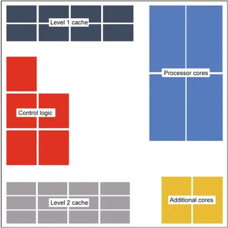
Interestingly, the machine-generated floorplans look nothing like those made by humans. Human designers typically arrange the macros in orderly rows and columns, often grouping related functions tightly together around the periphery of the chip while leaving interior areas open for standard cells.The result resembles grid-like apartment blocks separated by broad thoroughfares(Fig. 2). By contrast, Google’s automated floorplans appear almost random (Goldie has described them as ‘‘alien-looking” [9]): A patchwork of macros and open areas scattered across the chip with no obvious pattern.
The Google team said that its new method‘‘has the potential to save thousands of hours of human effort for each new [chip] generation” [1]. Andrew Kahng, professor of computer science and electrical engineering at the University of California at San Diego,added that ‘‘the development of methods for automated chip design that are better,faster,and cheaper than current approaches will help to keep alive the‘Moore’s Law’trajectory of chip technology” [5]. Moreover, because of its speed, the system can explore a much wider array of design possibilities than can human designers,who are limited by slow manual methods and tight schedules.

Fig. 2. Human floorplanners typically create orderly designs in which macros are grouped by function(processor blocks,memory,control logic,etc.).The open areas between the macro groups are then filled with smaller blocks of logic (standard cells) and interconnects (wiring that connects the various blocks).
The benefits appear to be more than theoretical. Google has promptly put its automated system to practical use, creating manufacturable floorplans for the company’s next-generation tensor processing units (TPUs). TPUs are application-specific integrated circuits (ASICs) designed to accelerate the machine learning systems vital to many Google services, including internet search, Street View, and Google Photos, as well as Google’s commercially available cloud-based AI services [10].
The Google team ultimately foresees a positive feedback loop in which machine learning speeds the development of more powerful chips, and the chips, in turn, accelerate machine learning. ‘‘In the past decade, systems and hardware have truly transformed machine learning,” said Mirhoseini [11]. ‘‘And it is now time for machine learning to return the favor and transform the way systems and hardware are designed.”
Chips may just be the beginning. ‘‘Placement optimizations of this form appear in a wide range of science and engineering applications, including hardware design, city planning, vaccine testing and distribution, and cerebral cortex layout,” said Mirhoseini et al. [1]. ‘‘Therefore, we believe that our placement optimization methodology can be applied to impactful placement problems beyond chip design.”
- Engineering的其它文章
- Supersonic Travel Seeks an Encore
- The Extremely Low Frequency Engineering Project for Underground Exploration
- The Dual Regulatory Roles of Macrophages in Acute Allogeneic Organ Graft Rejection
- Role of Intrahepatic Regional Immunity in Post-Transplant Cancer Recurrence
- In Vivo Development of Fetal Pig Kidneys in Mature Monkeys under Clinically Approved Immunosuppressant Drugs
- Two-Layer High-Throughput: Effective Mass Calculations Including Warping

