Realization of semiconducting Cu2Se by direct selenization of Cu(111)*
Yumu Yang(杨雨沐), Qilong Wu(吴奇龙), Jiaqi Deng(邓嘉琦), Jing Wang(王静), Yu Xia(夏雨),Xiaoshuai Fu(富晓帅), Qiwei Tian(田麒玮), Li Zhang(张力), Long-Jing Yin(殷隆晶),Yuan Tian(田园), Sheng-Yi Xie(谢声意), Lijie Zhang(张利杰), and Zhihui Qin(秦志辉)
Key Laboratory for Micro/Nano Optoelectronic Devices of Ministry of Education&Hunan Provincial Key Laboratory of Low-Dimensional Structural Physics and Devices,School of Physics and Electronics,Hunan University,Changsha 410082,China
Keywords: Cu2Se, scanning tunneling microscopy, scanning tunneling spectroscopy, semiconducting, selenization
1. Introduction
The discovery of graphene ignited the research of other two-dimensional (2D) materials with exotic properties.[1-4]For instance, elemental 2D materials such as silicene,[5-7]germanene,[8-13]stanene[14]and bismuthene[15]are predicted to exhibit quantum spin Hall effect, which would have application in low-power electronics to fault-tolerant quantum computing.[16]Transition metal dichalcogenides (TMDs) are typical 2D materials with intriguing properties like tunable bandgaps and inherently stronger spin-orbit coupling, which can be exploited for various device applications.[17-20]Bulk group IB transition metal chalcogenides are well known for their thermoelectric properties especially the application for solar cells materials.[21]Recently, 2D form of group IB transition metal chalcogenides starts to receive attention although their bulk parent materials are not layered. Shahet al.[22]confirmed the formation of honeycomb structure of AgTe, and¨Unzelmannet al.[23]found experimentally the Rashba-type spin splitting in different bands of AgTe related to the existence of orbital angular momentum.CuSe is a fascinating transition metal monochalcogenide that has been calculated to host the Dirac nodal line fermion, protected by mirror reflection symmetry.[24]It has been reported that CuSe can be grown on Cu(111).[25]However, the fabricated monolayer CuSe shows varying features, such as, with intrinsic nanopores[25]and in 1D moir´e pattern.[24,26]Walenet al.systemically investigated low coverage of Se on Cu(111) forming variable overlayer structures.[27]Cu2Se has long been known to be an excellent thermoelectric material serving as energy storage. It is also quite important for the synthesis of a class of thin film solar cells, Cu(In, Ga)Se2(CIGS).[28]Layered structure of Cu2Se was raised recently.[29]Previous reports have shown the fabrication of Cu2Se by co-evaporation of Cu and Se and found the phase transformation with pure thermo driven.[30]Wanget al.developed a straightforward way to synthesis PtSe2by direct selenization of Pt(111).[31]Based on this strategy, a few reports have shown the feasibility of fabricating new layered structures without layered bulk counterpart.[32-34]With this regards, direct selenization of Cu to form Cu2Se has not been reported yet.
Here, we report the synthesis of large-scale monolayer Cu2Se by direct selenization of Cu(111). Scanning tunneling microscopy and spectroscopy (STM/STS) were employed to explore its structural and electronic properties. X-ray photoelectron spectroscopy (XPS) data reveals the composition of the sample as Cu2Se. First-principles calculations indicate monolayer semiconductor Cu2Se with an indirect band gap of 0.8 eV,which agrees quite well with the STS measurement.
2. Experimental and theory details
The sample was fabricated by physical vapor deposition of Se on Cu(111) in a ultrahigh vacuum (UHV) chamber equipped with an STM (Unisoku). The base pressure of the system is below 2.0×10⁻¹⁰mbar. Prior to the Se deposition,Cu(111)(purchased from MaTeck)was cleaned via cycles of argon-ion(1.2µA,1 kV)sputtering followed by annealing at~550°C.Molecular beams of Se(99.999%,Alfa Aesar)were deposited onto the clean Cu(111) surface from a home-built evaporator. During the evaporation the substrate was kept at room temperature whereas the pressure of the vacuum chamber went to 10−7mbar. We calibrated the Se deposition rate by checking the condition of overlayer coverage on Cu(111)surface. Here, in our experiment, more than one monolayer amount of Se has been deposited on the substrate.All the STM measurements were performed at room temperature.Differential conductance(dI/dV)spectra were acquired by a standard lock-in amplifier at a frequency of 973 Hz with a 50 mV modulation. The tip calibration was performed on an Au(111)substrate.
The calculations were performed within the projected augmented wave formalism[35]as implemented in the Viennaab-initiosimulation package (VASP).[36,37]To calculate the electronic structure of Cu2Se, we used the GW0 scheme.[38]The initial Green’s functions were calculated using density functional theory (DFT) within the generalized gradient approximation,[39]and self-consistently iterated four times, which is sufficient to achieve numerical convergence.The screened Coulomb interaction was calculated at the full RPA level, and not updated during the calculation. To this end,we performed a numerical integration over the frequency axis with 50 grid points. In the calculation of the quasiparticle energies,both diagonal and off-diagonal elements of the selfenergy matrix were considered. In all calculations, we used an energy cutoff of 400 eV for the plane-waves,and a convergence threshold of 10−8eV.The number of unoccupied states in GW calculations was set to 700 per unit cell, which spans an energy interval of around 90 eV. The Brillouin zone was sampled by a(4×4)k-point mesh. In order to avoid spurious interactions between the Cu2Se layers in the nonperiodic direction, a 30 ˚A thick vacuum slab was added in the direction normal to the Cu2Se layer. The crystal structure of Cu2Se was adopted from Ref. [30], with the lattice constant 4.0 ˚A. We checked that the numerical parameters ensure that the quasiparticle gap is accurate to within 10 meV.
3. Results and discussion
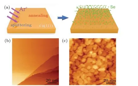
A schematic sample preparation process is shown in Fig. 1(a). Prior to Se deposition, an atomic clean Cu(111)substrate is required. Large-scale empty state STM image of Cu(111) substrate is shown in Fig. 1(b). Clear Cu step edges are visible revealing the cleanness of the substrate. Afterwards, we deposited a few monolayers of Se on the substrate. The surface was dramatically modified and covered by full of protrusions (see Fig. 1(c)). We cannot get high resolution STM images at this condition since the unlikely formation of ordered structure without annealing. Subsequently,we annealed the sample mildly at a temperature of~200°C for 10 min. Figure 2(a) shows a large-scale STM image of the surface, which contains a few ordered structural terraces with hexagonal-like shape. The height difference of these terraces is~0.2 nm(see the line profile in the inset of Fig.2(a)),which is in good consistence with the step height of Cu(111)single crystal. We zoom-in on a random position of the terrace(marked by a green square),a clear moir´e pattern with a periodicity of 3.7 nm is visible. Further zoom-in small-scale atomic resolution STM image is shown in Fig. 2(c). A line profile indicates the periodicity of the structure, revealing the lattice constant of~0.4 nm. Fast Fourier transform (FFT),presented in the inset of Fig.2(b)shows clear double periodicities,which agrees quite well with the measured ones.

Fig.1. Fabrication process of Cu(111)selenization. (a)Schematics of the substrate cleaning and Se deposition. (b) Large scale STM image of a clean Cu(111) (set points: sample bias 1 V and tunneling current 100 pA). (c) STM image of the surface after a few monolayers of Se deposited on the surface before annealing(scanning parameter: sample bias 1 V and tunneling current 2 pA).
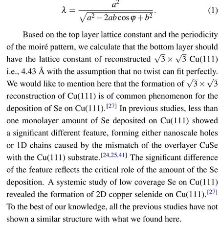
Moir´e pattern can be formed either by the lattice mismatch and/or the rotation of stacked periodic structure layers.We analyzed the relations of the hexagonal moir´e pattern superstructure wavelength and the precise atomic lattice structure of the overlayer and found that the bottom layer should also be a hexagonal shape. The relation of the given lattice constants of the stacking layersa(top) andb(bottom), the relative rotation angleϕ, and the moir´e wavelengthλcan be described as follow:[40]

Therefore,STS measurements were performed to explore the electronic properties of the synthetic overlayer.Figure 2(d)shows the distinctive differential conductivity (dI/dV) spectra, recorded on top of the overlayer at different positions.According to the dI/dVcurve, we deduce its conductive band minimum (CBM) and valence band maximum (VBM)at 0.70 eV and−0.08 eV, respectively. These values altogether give a quasi-particle band gap of~0.78 eV. There is no obvious variation of all the dI/dVcurves performed on other positions of the overlayer, revealing uniform electronic properties of the synthesized monolayer structure. The finding of semiconducting feature here is obviously different from the previous formed CuSe on Cu(111),[24]where combined DFT calculations and angle resolved photoemission spectroscopy(ARPES)measurements have revealed its metallic properties. Furthermore, our measured band gap is also significantly larger than the value obtained by Guoet al.on CuSe/Cu(111) recently.[41]Hence, we carefully exclude the possibility of forming CuSe in our case. Recently,a new layered structure of Cu2Se has been raised by Nguyenet al.[29]Based on the theoretical calculations,they found that the new structure of Cu2Se is energetically,dynamically and mechanically stable. Furthermore, they also found that Cu2Se has a band gap of 0.74 eV,[29]which is quite close with our experimental results. Because of these stability and layered nature,the newly proposed Cu2Se structure can be fabricated on substrate. With a careful scrutiny of the structural and electronic properties of the obtained structure, we find that this newly reported structure Cu2Se can fits our findings quite well. Interestingly, recently Qianet al.co-deposited Se and Cu in ultra-high vacuum condition on bilayer graphene terminated of SiC substrate.[30]They proposed the synthesized structure asλ-phase of Cu2Se at room temperature. The top Se atoms were resolved by STM as a triangle/hexagonal shape.

Fig.2. The atomic structure and electronic properties of Cu2Se. (a)A large scale STM image(sample bias 1 V and tunneling current 10 pA)of Cu2Se.A line-profile across the step edge presented in the inset with a height of around 0.2 nm. (b) A zoom-in STM image (sample bias 700 mV and tunneling current 100 pA)of Cu2Se. Image inset is the FFT at(b). (c)Atomic configuration of Cu2Se at the top panel and the lower panel is the line-profile of Cu2Se. (d) dI/dV spectra of Cu2Se indicating a semiconducting feature with a band gap of 0.78 eV.

Fig.3. The core level XPS spectrum of Cu2Se sample on Cu(111)substrate.(a)Two peaks can be resolved in the Se 3d signal,54.3 eV and 55.0 eV.(b)Two well-defined peaks of Cu locate at 932.5 eV and 952.4 eV.
In order to further verify the composition of the synthesized sample,we performed x-ray photoelectron spectroscopy(XPS)on the surface.Monochromatic radiation light was realized by four high resolution gratings and controlled by a hemispherical energy analyzer that possesses a photon energy in the range from 10 eV to 1100 eV.High-resolution XPS spectra of Cu 2p and Se 3d regions are plotted in Figs.3(a)and 3(b). The binding energies of Cu 2p3/2and Cu 2p1/2are 932.5 eV and 952.4 eV,respectively. It demonstrates that the 932.5 eV peak can be ascribed to Cu+ions.[42]In addition, compared with the XPS data of Cu2−xSe,the binding energy peak position of Se 3d5/2in our case is quite different.[43]However,our results are in good agreement with the XPS data of Cu2Se reported recently,[30,44]revealing that the composition of the sample is indeed Cu2Se.
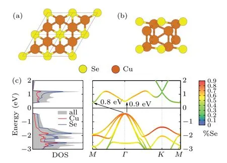
First-principles GW calculations were carried out to further clarify the electronic properties of the synthesized Cu2Se.Figures 4(a) and 4(b) show ball and stick models of top and side views of Cu2Se, where yellow balls represent Se atoms and brown ones are Cu atoms. The model was inspired by Ref. [30], from which we adopt theλ-phase of Cu2Se. In the calculation, we consider an isolated monolayerλ-Cu2Se and investigate its electronic properties.The calculated project density of state reveals an indirect band gap of~0.8 eV,which is in accordance with our STS measurement of 0.78 eV.Deviation of the band gap between the theoretical calculation and the experimental results can be attributed to the Cu(111)substrate screening,which is neglected in our calculations.Therefore, the calculations provide additional evidences regarding the fabrication of monolayer Cu2Se.

Fig. 4. First-principles GW calculations of monolayer Cu2Se. (a)Top and (b) side views of monolayer Cu2Se structure. (c) Density of states(DOS)and band structure calculated in this work within the GW0 scheme for monolayer Cu2Se. Red and blue lines in DOS correspond to the contributions of Cu and Se states, respectively. The color bar indicates the contribution of Se states in the band structure.
4. Conclusion
In summary, we deposited a few monolayers Se on Cu(111) to form Cu2Se, a new layered 2D transition metal chalcogenide material. Combining STM/STS, XPS and the first-principles calculations, we confirmed the synthesized overlayer of Cu2Se.Differential conductivity reveals the semiconducting properties. The formed moir´e pattern origins from the mismatch of Cu2Se overlayer and underlayer Cu(111)but no moir´e potential related electronic states were found. Firstprinciples calculations verified the semiconducting properties which agrees quite well with scanning tunneling spectroscopy results. This work indicates the successful synthesis of Cu2Se by direct selenization of Cu(111), which paves a way of the fabrication of group IB transition metal chalcogenides.
- Chinese Physics B的其它文章
- Numerical investigation on threading dislocation bending with InAs/GaAs quantum dots*
- Connes distance of 2D harmonic oscillators in quantum phase space*
- Effect of external electric field on the terahertz transmission characteristics of electrolyte solutions*
- Classical-field description of Bose-Einstein condensation of parallel light in a nonlinear optical cavity*
- Dense coding capacity in correlated noisy channels with weak measurement*
- Probability density and oscillating period of magnetopolaron in parabolic quantum dot in the presence of Rashba effect and temperature*

