Temperature Dependence and Evolution Mechanism of Aluminum Nitride Morphologies
NIU Hui-dan, KONG Su-su, YANG Shao-yan*, LIU Xiang-lin,WEI Hong-yuan, YAO Wei-zhen, LI Hui-jie, CHEN Qing-qing, WANG Lian-shan, WANG Zhan-guo
(1. Key Laboratory of Semiconductor Materials Science, Institute of Semiconductors, Chinese Academy of Sciences, Beijing 100083, China; 2. Center of Materials Science and Optoelectronics Engineering, University of Chinese Academy of Sciences, Beijing 100049, China)*Corresponding Authors, E-mail: sh-yyang@semi.ac.cn; xlliu@semi.ac.cn
Abstract: Aluminum nitride(AlN) is a significant ultra-wide bandgap semiconductor material. This paper studies the surface morphology evolution and growth mechanism of AlN grown on sapphire substrates by hydride vapor phase epitaxy(HVPE). The morphologies of AlN are controlled by the nitridation pre-treatment and the growth temperature from 750 ℃ to 1 100 ℃. The results show that growth temperature played a critical role in the AlN growth of morphology and growth mode. The difference in nanoscale or microscale morphologies of AlN is attributed to the surface migration of Al adatoms dominated by the growth temperature and the evolution of the dislocation. Moreover, the surface morphology evolution leads to an inverted pyramid morphology or large V-shaped pits at the growth temperature of 900 ℃. The grown V-shaped pits have {10-11} semi-polar facets and follow the three-dimensional(3D) growth mode. The semi-polar facets AlN structure could be used for realizing facet-controlled epitaxial of semi-polar UV-LED or other Ⅲ-nitride growth, which has prospects in optoelectronic and electronic devices.
Key words: ultra-wide bandgap semiconductor; aluminum nitride; hydride vapor phase epitaxy; growth temperature; surface morphology
1 Introduction
AlN is a significant ultra-wide bandgap semiconductor material with a direct bandgap of 6.2 eV, which has great prospects for deep ultraviolet optoelectronic devices and power electronic devices[1-4]. Due to the matching lattice and thermal expansion coefficient, AlN is the promising substrate material or the buffer layer for the epitaxial growth of group Ⅲ-nitrides devices[5-8]. However, it is difficult to obtain high-quality single-crystalline, and crack-free AlN with low threading dislocation density(TDD). Hydride vapor phase epitaxy(HVPE) is a promising method used to synthesize group Ⅲ-nitride materials on foreign substrates[9-10]. Many advantages include simple equipment, rapid growth, large-area growth, and reducing dislocation density. However, some problems still need to be overcome to improve the AlN epitaxial growth quality. For example, the temperature of HVPE growth was limited to 1 200 ℃ due to the melt temperature of quartz tube reactor[11-12].
Many researchers have focused on the crystalline quality and surface morphology of AlN[13-18]. The growth conditions have a remarkable influence on the properties and morphologies of group Ⅲ-nitride materials for electrical and optoelectronic devices[19-21]. Among them, V-shaped pit defects have been found to improve the electroluminescence properties of Ⅲ-nitride light-emitting diodes(LEDs)[22]. Rathkanthiwaretal.demonstrated that the V-shaped pit morphological defects influenced the dark current and spectral responsivity for AlGaN UV-B photodetectors with the AlN buffer layer[23]. Lietal.reported that V-shaped pits in AlGaN MQWs on AlN templates might affect optical influences for DUV emission[24]. The V-shaped pit is a common structural defect in group Ⅲ-nitrides epitaxial layer, which is like an inverted hexagonal pyramid with six {10-11} side facets extending from the(0001) plane[25]. This surface pit is usually obtained under high temperature or low Ⅴ/Ⅲ ratio, originating from the threading dislocations. It is important to figure out the evolution of the V-shaped pits on the AlN surface and the behavior of how to arise the {10-11} semi-polar facets.
In this work, the surface morphology evolution of AlN growth was investigated based on different growth temperatures from 750 ℃ to 1 100 ℃. The AlN grew onc-plane sapphire substratesviaHVPE equipment. By tuning the growth temperature, the AlN epitaxial layers were different in nanoscale to microscale morphologies. The V-shaped pits were generated by the evolution of dislocation and the coalescence of the grains at 900 ℃. A surface diffusion-based mechanism explained the formation of the microscopic structure. During the AlN epitaxial growth process, the migration of Al adatoms would significantly influence the quality and surface morphology of AlN growth. Due to the lower surface mobility of Al adatoms, the short diffusion length of Al adatoms resulted in 3D islands growth on the AlN surface morphology. Moreover, the growth model has a transition from 3D to 2D mode in a higher temperature by enhancing the diffusion length of Al adatoms.
2 Experiments
2.1 Materials Growth
The AlN samples were grown in our homemade HVPE horizontal growth equipment. The HVPE reactor consisted of two independent heated zones: the source zone and the growth zone. At first, HCl gas flew over metal Al boat forming AlCl3as Al source in the source zone at 550 ℃. Next, ammonia(NH3) gas was used as the N source. AlN was grown on 2-inch sapphire wafers with thec-plane surface at the high-temperature growth zone. During the AlN growth process, nitrogen(N2) was introduced to the reactor as carrier gas. The growth zone for AlN was limited to a range from 750 ℃ to 1 100 ℃. The total gas flow rate was 3 600 cm3/min(standard cubic centimeter per minute) to keep the pressure at 1.33×10⁴Pa(100 Torr).
The detailed growth process is as follows. Heat treatment in hydrogen was conducted at 1 100 ℃ for 10 min, removing contaminants from the surface of sapphire substrates. Then, the nitridation process was pretreated by NH3gas flow for 3 min. During the growth step, the reaction chamber was heated to the set temperature. The NH3gas flow was set at 500 cm3/min, and the HCl gas flow was set at 100 cm3/min to grow the AlN epitaxial layer for 60 min, in which the Ⅴ/Ⅲ ratio is about 15. When the growth process finished, the reactor was allowed to cool down naturally to room temperature flowing NH3and N2gas.
2.2 Materials Characterization
The morphology of samples was studied using scanning electron microscopy(SEM: FEI NOVA NanoSEM 650). The crystal structures were characterized by X-ray diffraction analysis(XRD: Rigaku SmartLab, Cu Kα) and Raman spectroscopy(Lab-RAM HR Evolution, 532 nm solid state laser as the excitation source) at room temperature.
3 Results and Discussion
3.1 Growth Process and Mechanism of AlN
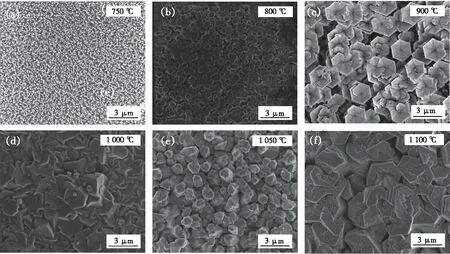
AlN samples were grown at various temperatures from 750 ℃ to 1 100 ℃ after pre-treatment nitridation, the morphologies shown in Fig.1. When the growth temperature was 750 ℃, the AlN displayed a high-density nanoneedle array perpendicular to the sapphire substrate, as shown in Fig.1(a). The diameter of nanoneedles gradually decreased along with thec-axis orientation. While the temperature was 800 ℃, the AlN nanocolumns were found, as shown in Fig.1(b). The diameter of AlN was significantly larger compared with the sample of 750 ℃. However, both AlN of 750 ℃ and 800 ℃ were still one-dimensional nanoscale structures. When the growth temperature increased to 900 ℃, the AlN changed to hexagonal micro-pillars, as shown in Fig.1(c), forming a V-shaped pit on the top of the micro-pillar simultaneously. While the temperature further reached 1 000 ℃, the AlN merged as a single-crystalline thick film, as shown in Fig.1(d). The growth conditions of AlN under 1 050 ℃ and 1 100 ℃ were also provided in Fig.1(e) and(f).

Fig.1 SEM images of the AlN samples grown at different temperatures.(a)AlN nanoneedles were grown at 750 ℃.(b)AlN nanocolumns were grown at 800 ℃. (c)AlN micro-pillars with hexagonal V-shaped pits were grown at 900 ℃. (d)AlN islands merged at 1 000 ℃. (e)AlN islands were grown at 1 050 ℃. (f)AlN islands were grown at 1 100 ℃.
The AlN growth in HVPE is a combination of atom transportation and surface reaction. In a large Ⅴ/Ⅲ ratio growth system, the diffusion of Al precursor plays an important role in the growth of AlN[26].
A surface diffusion-based mechanism[27-28]was correlated with the diffusion length of Al adatoms, which was directly influenced by growth temperature. When the growth temperature was higher, the diffusion length of Al adatoms should be farther. The chemical reaction rate on the surface was very fast actually, in which the precursors reaching the substrate were reacting quickly and actively to grow. Hence, the AlN growth was dependent on the mass transport, namely the transportation rate of the precursors to the substrate surface.
The AlN growth followed the vapor-solid(VS) growth model[29]including three stages of gas transport, gas-phase reaction and surface reaction. In the nitridation pre-treatment process, the O atoms at the sapphire surface were substituted by the N atoms from NH3. In the gas transport process, the Al source of AlCl3reacted from HCl vapor with Al was carried by N2gas. And then, AlCl3and NH3would mix to flow in the high-temperature growth zone[30]. Macromolecules [AlN]n(n=integer) present with Al—N bond as the backbone developed into nanoclusters for gas-phase reaction. These nanoclusters in gas-phase were adsorbed or aggregated to substrate surface, forming a certain density of randomly distributed nuclei.
Subsequently, the N or Al atoms or their molecules were absorbed into the nuclei for the 2D step and 3D island growth models. In the surface adatoms diffusion process, the adatoms migration determined the size of isolated island and the microcosmic morphology. Hence, the surface reaction decided the growth conditions of AlN. Gas-phase and surface reactions were mutually reinforcing steps for the AlN growth. And the growth temperature had a powerful influence on the two steps. Such as the low-temperature growth, the macromolecules [AlN]nhave a higher polymerization degree in the gas phase[31-32]. So the size of nuclei stopped growing larger in the initial nucleation process due to the poor surface diffusion mobility of Al adatoms.
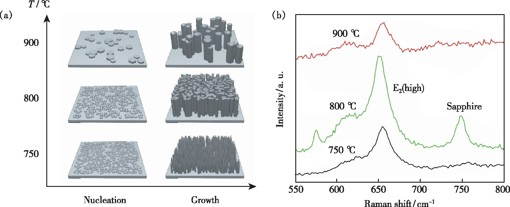
During the epitaxial growth process, the migration of Al adatoms would significantly influence the quality and surface morphology of AlN growth. The difference in growth rates along 2D step growth and 3D island growth resulted the various micro-nano structures of AlN. The temperature provided the thermal motivations for the nuclei to coverage and form grains, which influenced the size and density of crystal grains[33]. At a relatively low temperature, the migration of Al atoms was around the limited area of the substrate surface due to the strong binding energy of Al—N bonds. The Al—N bond strength is the intrinsic molecular property, regardless of temperature. When the growth condition was at a high temperature, the larger thermal motivation resulted in the enlarged diameter of nuclei and the lower nucleation density. In addition, the whole AlN tended to transition from 3D islands to 2D layer epitaxy. The schematic illustration of AlN growth about the VS growth model is shown in Fig.2(a). There formed AlN nanoneedles at 750 ℃. The density of nuclei on substrate surface and the lateral growth of AlN were not sufficient to coalesce into a whole film. The growth temperature over 800 ℃ in the reaction chamber was high enough to motivate the AlN nuclei to gather into hexagonal grains. The Raman spectra of AlN samples with different growth temperatures are shown in Fig.2(b), forming the AlN micro-nano structures. It displays thec-facet strain of AlN samples. With the temperature increasing, the E2(high) mode near 655 cm-1was right shift at 900 ℃ compared to the result at 800 ℃. The shift is due to the in-plane compression biaxial stress of AlN that leads to the changes in phonon frequencies[34-35]. Hence at 750 ℃ and 800 ℃, the nanometers diameter surface is relatively small, relieving the stress caused by lattice mismatch with the sapphire substrate. With the further increase of temperature to 900 ℃, the compressive stress was produced when the AlN pillars were aggregating into large islands,and then the top surface was split into V-shaped pits.

Fig.2 (a)Schematic illustration of the VS growth model for nitridation pre-treatment method in different growth temperatures, forming the AlN micro-nanostructures. (b)Raman spectra of AlN samples with different growth temperatures.
In contrast, AlN grown at 1 000 ℃ exhibited continuous film morphology. Some irregular mound-like structures on the substrate were caused by the large viscosity coefficient of Al atoms because the empty Al—N bonds were stronger to catch Al atoms.
The anisotropic crystal structure and chemical bonds determined the competitiveness of the preferred growth. When the mobility of Al atoms was larger at 1 000 ℃, the Al atoms easily enhanced the lateral growth of AlN to form crystal grains. Then the grains sharing a similar crystal orientation tended to converge with each other. The combination of adjacent grains was motivated by reducing broken bonds of the interface to lower the whole surface energy. The corresponding X-ray diffraction(XRD) patterns are in Fig.3, showing a prominent(0002) peak of the wurtzite AlN along with an obviousc-axis orientation. So the growth behavior about the preferred orientation is along {0001} direction of AlN epilayers at different growth temperatures. According to Van der Drift’s competition mechanism for growth orientation, the [0001] direction of AlN, perpendicular to the substrate, has the fastest growth rate[36]. Due to their different dangling band density and crystal lattice, this growth behavior was mainly controlled by kinetics. Also, the high temperature could increase the diffusion length of N, Al atoms, and their clusters towards the surface energy equilibrium. The orientated AlN grains, perpendicular to the sapphire surface, were easier to catch the atoms and clusters.

Fig.3 XRD pattern of AlN samples at varied growth temperatures with inset of FWHM. (a)750 ℃. (b)800 ℃. (c)900 ℃. (d)1 000 ℃. (e)1 050 ℃. (f)1 100 ℃.
3.2 Surface Morphology Evolution of V-shaped Pits
The V-shaped pits appeared on the surface of AlN micro-pillars at a growth temperature of 900 ℃ after the nitridation pre-treatment. Fig.4(a) shows the schematic structure of the V-shaped pits composing of six equivalent semi-polar {10-11} facets. The XRD pattern of the AlN in Fig.3(c) shows a prominent (0002) peak and a weak (10-11) peak, indicating that the micro-pillars mainly grew along with the [0001] direction. The stability of the crystal planes related to the {10-11} facets of the AlN micro-pillars, as shown in Fig.4(b). Fig.4(c) shows the SEM images of the inverted pyramid structure on the (0001) plane of the AlN micro-pillars with a microscale surface morphology. The structure is a hexagonal and symmetrical V-shaped pit, of which each facet has equal inclinations to the (0001) plane. Fig.5(a)-(c) present the SEM images of different views, showing that the hexagonal AlN micro-pillars have about 2.31 μm diameter and 7.87 μm length. The density of V-shaped pits is about 0.25 μm-2.

Fig.4 Schematic illustration and characterization of AlN micro-pillars with V-shaped pits grown at 900 ℃. (a)Schematic diagram of the hexagonal V-shaped pits. (b)Schematic illustration of the charge equilibrium for semi-polar surfaces is based on the alternating positive and negative charges. (c)SEM images of AlN micro-pillars with V-shaped pits on the top surface.

Fig.5 SEM images of AlN micro-pillars with V-shaped pits. (a)Surface image with a detail view inset of V-shaped pit.(b)Tilt-view image. (c)Cross-section image.
The mechanism of generating V-shaped pits was investigated for morphology evolution, which could be interpreted by the islanding and coalescence process of AlN growth. The AlN islands were formed at the nucleation step and prepared for 3D growth mode. These islands would gradually coalesce as crystal seeds, recrystallized into hexagonal grains in the initial growth stage. However, the heteroepitaxy of AlN on sapphire substrates led to a high dislocation density due to large thermal and lattice mismatches between them[37]. Some of the dislocations would get annihilated in the process of lattice merging by forming dislocation loops[38-39]. Others were still grown through the AlN layer to form the threading dislocations[40-41]. The threading dislocation development promoted the formation of the V-shaped pits. The unvanished threading dislocations were difficult to adsorb gas molecules. Then they gradually formed the centers of V-shaped pits.
The evolution of the semi-polar facets was attributed to the adatoms diffusion and the surface energy equilibrium in the anisotropic structure of wurtzite AlN. The huge electronegativity difference between Al and N resulted in a strong polar covalent bond. So the adatoms significantly influenced the surface polarity. In the AlN structure, the surface energy of the polar (0001) plane was higher than the semi-polar (10-11) facets of the V-shaped pit[42]. The semi-polar facets could reduce the internal polarization and surface polarity of AlN, which lowered the surface energy. As shown in Fig.4(b), the charge equilibrium model, illustrated that the AlN growth was inclined to satisfy the lowest surface potential energy. Hence, the top surface was transformed into semi-polar facets during the growth process to achieve charge equilibrium and lower surface energy than the plain (0001) plane.
4 Conclusion
In conclusion, the AlN was grown in a temperature range from 750 ℃ to 1 100 ℃ in our homemade HVPE system. The results revealed that nanoscale AlN could be grown at low temperature below 900 ℃ due to the poor surface migration of Al adatoms. The higher temperature was favorable to surface mobility of Al adatoms and lateral growth, resulting in that the AlN morphology changed to microscale combination. Moreover, the morphology evolution of the V-shaped pits with inverse pyramid structure was related to threading dislocation development and surface energy equilibrium. Therefore, the temperature of V-shaped pit formation was probably limited to a narrow temperature range. How to realize the V-shaped pits array need to be further explored, which could be used as the templates on optoelectronic and electronic devices.
Response Letter is available for this paper at:http://cjl.lightpublishing.cn/thesisDetails#10.37188/CJL. 20210287.

