Perovskite Single Crystals:Synthesis,Properties,and Applications
Shan-Shan Rong | M.Bilal Faheem | Yan-Bo Li
Abstract—Perovskite single crystals have gained enormous attention in recent years due to their facile synthesis and excellent optoelectronic properties including the long carrier diffusion length,high carrier mobility,low trap density,and tunable absorption edge ranging from ultra-violet (UV) to near-infrared (NIR),which offer potential for applications in solar cells,photodetectors (PDs),lasers,etc.In this review,we summarized the synthesis,properties,and applications of organic-inorganic mixed and all-inorganic perovskite single crystals,particularly those through the solution synthesis approach.Challenges towards the crystal growth and stability with future perspectives were also briefly described at the end of this paper.
1.lntroduction
Calcium titanate (CaTiO3) was named perovskite after the Russian mineralogist,Count Lev Aleksvich Perovski[1],which represents a particular type of crystal structure.Organic-inorganic hybrid perovskite was first reported in 1978 and found to possess the similar structure as that of CaTiO3[2].Generally,the crystal structure of metal halide perovskite is denoted as ABX3,where A is either organic CH3NH3+(MA),CH7N2+(FA),or inorganic Cs+and Rb+cations,B is the Pb2+or Sn2+cation,and X is the halide anion (I–,Br–,and Cl–)[3]-[7].In the past decade,the perovskite materials have gained significant development in the photovoltaic and photoelectric fields due to their unique characteristics,such as the tunable bandgap[4],[8],high absorption coefficient[9],long charge carrier diffusion length,carrier multiplication[10],and high carrier mobility[4],[11]-[13].The efficiency of perovskite solar cells (PSCs) has been enhanced significantly to over 25.2% in the past decade[11],[14],[15],but the defect dynamics and grain boundaries within the polycrystalline perovskite thin films are major hurdles for further improvement of efficiency and stability of these devices.
Perovskite single crystals with outstanding photoelectric and optoelectronic properties bring hope due to the low defect density and absence of grain boundaries which are comparable to the best performing quality of silicon[13],[16]-[18].The properties of single crystals,such as high carrier mobility[19]-[21],long carrier diffusion lengths,and long carrier lifetimes[13],[17],[22],make single crystals more advantageous in solar cells[22]-[25],photodetectors (PDs)[26]-[28],light emitting diodes (LEDs),and lasers[29]-[31].For instance,solar cells based on single crystals obtained the best efficiency of 21.09% with a fill factor (FF) of 84.3% and predominate stability[32].PDs made of methylammonium lead bromide (MAPbBr3) single crystals achieved the responsivity(R) of 1.6 × 10⁴mA/W and external quantum efficiency (EQE) of about 3900%[19].These studies demonstrate that perovskite single crystals are promising building blocks for photoelectric conversion applications.In this review,we put our focus on the research progress in the synthesis,properties,and applications of hybrid (in majority of cases) and all-inorganic (in specific cases) perovskite single crystals in recent years.The methods to prepare perovskite single crystals with different compositions are first introduced.Next,the fundamental optoelectronic properties of the perovskite single crystals are summarized.Then,the outstanding performance of the single crystals in applications,such as PDs,solar cells,LEDs,and lasers,are presented.At last,the challenge and opportunity for applications of perovskite single crystals are proposed.
2.Synthesis Methods
The controllable synthesis of high-quality perovskite single crystals is of fundamental importance for their applications in the photovoltaic and photoelectric fields.While the methods used at earlier stages for the synthesis of perovskite single crystals are time consuming and challenging to obtain desired dimensions and properties,the effects have been devoted to developing more efficient synthesis methods for improving crystal quality[5],[13],[16],[17].Whereas high-quality and large-size crystals are still difficult to obtain,the methods to fabricate single crystals are essential and require a more focused approach from the research community.In this section,crystal growth strategies and fundamental principles for perovskite single crystals are summarized.
2.1.Solution Temperature Lowering (STL) Method
The solution temperature lowering (STL) method stems from the Weber’s method[33],which utilizes the difference of solubility of the perovskite precursors in solvents under different temperatures.The perovskite precursors are dissolved into the solvents at higher temperatures,then the temperature of the solution is gradually reduced to reach a supersaturated state which results in the growth of single crystals.For example,for the synthesis of methylammonium lead iodide (MAPbI3) single crystals,lead acetate trihydrate(Pb(CH2COOH)2·3H2O) and methylammonium iodide (MAI) were mixed in the hydriodic acid (HI) solution at 65 °C.The solution was saturated when the temperature decreased from 65 °C to 40 °C,and the well-shaped MAPbI3single crystals with a size of 10 mm × 10 mm × 8 mm were obtained[34],as shown inFig.1 (a).Sun’s group found that the incorporation of chlorine (Cl) into the precursor solution could improve the crystalline quality and reduce the growth time,and the MAPbI3(Cl) single crystal with a large size of 20 mm × 18 mm × 6 mm was synthesized using the modified STL method[35].
Besides the examples of the bottom-seeded STL method as described above[30],[33],[34],perovskite single crystals can also be grown by the top-seeded solution-growth (TSSG) method.The process of the TSSG method to grow MAPbI3single crystals is illustrated inFig.1 (b)and the image of the finally grown single crystal is represented inFig.1 (c)[13].In the TSSG method,lead acetate trihydrate and MA were dissolved separately in the HI solution at 100 °C.Then the MA solution was slowly added to the lead acetate trihydrate solution and the temperature of the mixed solution was decreased to 75 °C,which was kept for one day to grow small single crystals[12].After that,a silicon substrate was inserted vertically into the growth chamber.The nucleation of the crystal seed on the silicon substrate was facilitated by the removal effect of latent heat through an air-cooled silicon substrate on the top half of the chamber to form large-size crystals.Half of the silicon was kept outside the chamber to lower the temperature of the upper part solution that reduced the solubility of MAPbI3in the HI solution and the lower part of the bottle was kept at 75 °C with an oil bath.A 10-mm single crystal was grown in several days[12].
2.2.lnverse Temperature Crystallization (lTC) Method

Fig.1.Growth of perovskite single crystals:(a) picture of a MAPbI3 single crystal which exhibits the (100) and (112)planes[34];(b) schematics of the TSSG method;(c) MAPbI3 single crystal synthesized by the TSSG method[13];(d) ITC method and the growth process of the MAPbI3 single crystal[12];(e) MAPbX3 (X=Cl or Br) single crystals synthesized by the ITC method[36];(f) FAPbI3 single crystal synthesized by the ITC method[20];(g) schematic process of the LTGC method;(h) MAPbBr3 single crystal synthesized by the LTGC method[19].
In the process of the inverse temperature crystallization (ITC) method[21],[36],the precursor solution is put in a bottle and heated at a fixed temperature to grow single crystals,as illustrated inFig.1 (d)[12].During the growth process,at the beginning,the surface of the solution is in a saturated state because of the volatilization of the solvent,while the bottom of the solution is unsaturated.As the solvent decreases,the concentration will exceed the solubility of precursors because of the convection inside the bottle,which leads to the growth of single crystals.The pre-synthesized seed is used as a nucleation site for the growth of large single crystals.For example,for the synthesis of MAPbI3single crystals,the seed crystals were harvested by heating the precursor solution at 160 °C for 30 minutes.Next,a seed crystal was put into the precursor solution heated at 120 °C for 3 hours.Finally,a~8 mm MAPbI3single crystal was obtained.Moreover,largesize crystals could be obtained by increasing the solution temperature to 125 °C for another hour.By using the obtained large crystal as a seed again in the ITC process,even larger single crystals can be grown.The largest MAPbI3single crystal with the size of 71 mm × 54 mm × 39 mm was obtained by repeating the ITC process for several times[36].Similarly,large single crystals of MAPbBr3and MAPbCl3were also synthesized by this method,which are shown inFig.1 (e)[36].The growth will be faster if the temperature is higher,but the crystal will be malformed or small crystals will be formed when the temperature is too high.It should be noted that the crystal will be re-dissolved if the temperature decreases to room temperature[20],[36].Therefore,the single crystals should be harvested before cooling the solution.This method is suitable for the preparation of multi-component single crystals,such as FAPbI3(shown inFig.1 (f)[20]),MAPbCl3,MAPbIxBr1–x,and MAxFA1–xPbI3crystals[12],[21],[37].
The ITC method was combined with a low-temperature-gradient crystallization (LTGC) method to grow the large MAPbBr3single crystal (as shown inFig.1 (g))[19].The precursor solution was put in a sealed bottle and the temperature of the solution was increased gradually with a temperature gradient of 2 °C/day.The solution was saturated during the process,resulting in the growth of the single crystal.A single crystal with the size of 44 mm × 49 mm × 17 mm (Fig.1 (h)[19]) was grown in 18 days and showed an extremely low trap density of 5.2 × 109cm–3.
2.3.Anti-Solvent Vapor-Assisted Crystallization (AVC) Method
The anti-solvent vapor-assisted crystallization (AVC) is a reproducible and temperature independent method to grow high-quality single crystals by utilizing the solubility of the precursor solution in different solvents.It was developed by Bakr’s group[17]to grow crack-free MAPbBr3single crystals with the volume exceeding 100 mm3.The process of AVC is represented inFig.2 (a).The precursor is put into a sealed bottle containing antisolvent,and the solubility of the mixed solvent decreases when the antisolvent is diffused into the precursor solution,resulting in the growth of crystals.Taking MAPbBr3for example,firstly,MABr and PbBr2were dissolved in dimethylformamide (DMF) with a molar ratio of 1:1 to prepare the precursor solution.Then the precursor solution was put in a small bottle which was sealed in the atmosphere of dichloromethane(DCM).Finally,the crystals were grown with DCM diffusing into the precursor solvents,which is attributed to the decreased solubility of the mixed DMF-DCM solvent.Generally,the precursor solution should have good solubility of solvents[17],[38],such as DMF,gamma-butyrolactone (GBL),and dimethyl sulfoxide (DMSO).Antisolvents are completely insoluble towards MAPbX3[17],[39],such as DCM,acetonitrile,and chlorobenzene (CB).Based on this method,Fang et al.modified the diffusion speed of DCM,for which the precursor solution was sealed with a small hole left to let DCM enter slowly[38].At last,crystals with the size of several millimeters were obtained.The AVC method was also utilized to prepare all-inorganic CsPbBr3single crystals[40].DMSO and MeOH were used as the solvent and antisolvent,respectively,and,a single crystal with the dimension of 42 mm × 5 mm × 3 mm was obtained.
Moreover,the molar ratio of MABr/PbBr2will affect the anisotropy of crystals,which causes the appearance of polyhedron MAPbBr3crystals,as shown inFigs.2 (b)and(c)[39].Wei et al.also found that the 1:1 molar ratio of MABr and PbBr2caused defects on the crystal surface,due to the different solubility of precursors in DMF[41].This issue was resolved successfully by using a 1.0:0.8 ratio of MABr and PbBr2,and high-quality large-size single crystals were obtained,as shown inFig.2 (d)[41].
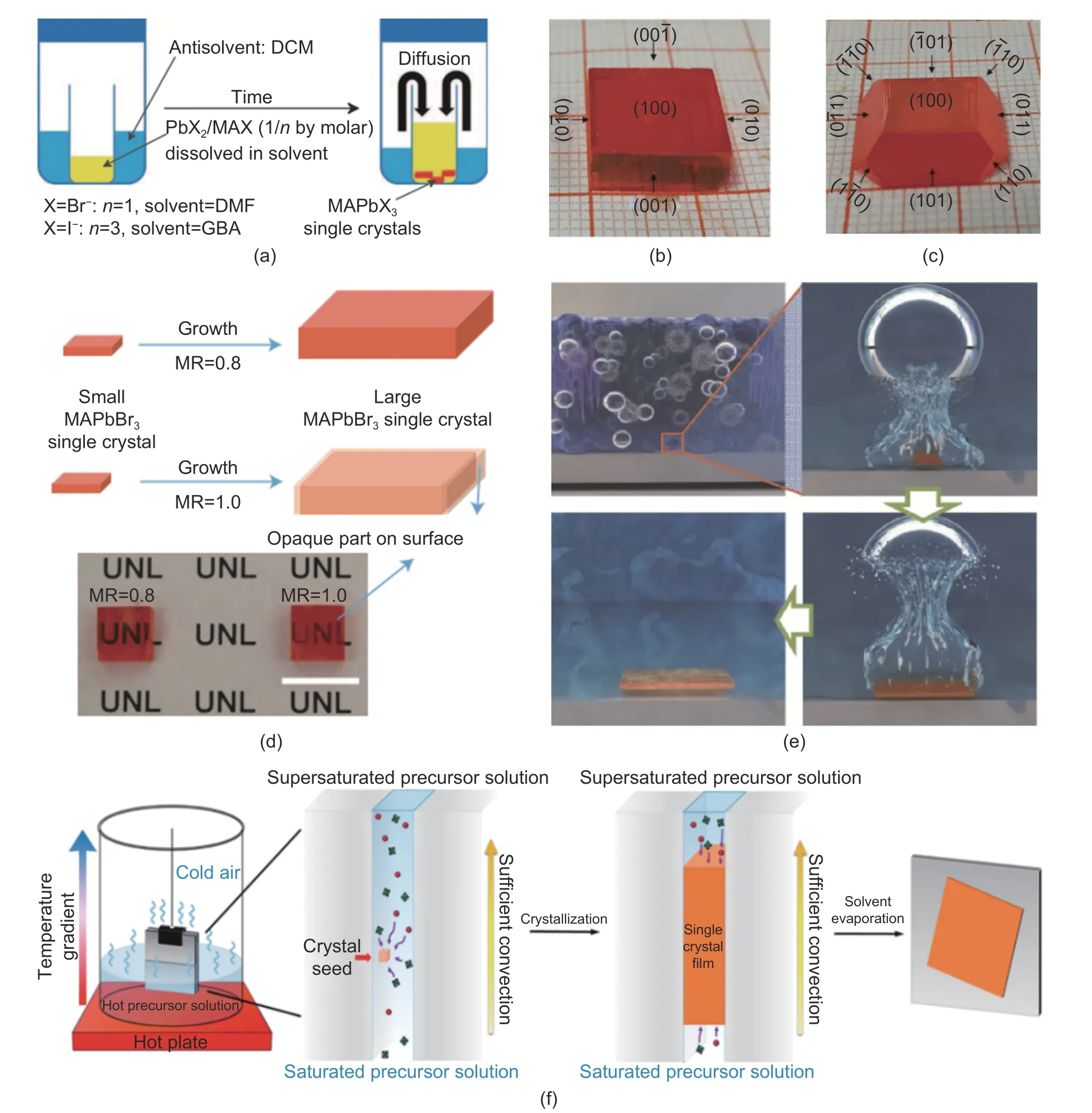
Fig.2.Controlled growth of single crystals:(a) schematic diagram of the AVC method[17];(b) cubic and (c) polyhedral MAPbBr3 single crystals obtained by the AVC method[39];(d) single crystals of MAPbBr3 grown with different molar ratios of PbBr2/MABr[41];(e) cavitation-triggered asymmetrical crystallization (CTAC) strategy for the growth of MAPbBr3 monocrystalline[42];(f) schematic illustration of the SLITC method for the growth of single-crystal wafers.
2.4.Thickness Controllable Methods
With the development of preparation methods for perovskite single crystals,controlling the thickness has become a challenge,because the thickness of single crystals influences the device application significantly.The thickness controllable methods of single crystals mainly include the cavitation-triggered asymmetrical crystallization (CTAC) strategy[42],facile solution-processes method[43],[44],vertical Bridgman technique[45],space-limited inverse temperature crystallization (SLITC),and ligand-assisted precipitation method[43],[46].The CTAC method was developed by Bakr’s group,which introduced the ultrasonic pulse to the growth process of MAPbBr3monocrystalline,as shown inFig.2 (e)[42].The large bulk and uneven distribution on the surface of single crystals hinder the further research,which is due to the higher nucleation energy barrier.Through ultrasonic pulses,the nucleation on the surface was promoted on the low supersaturation level,increasing the pressure and energy accumulation,which is attributed to the cavitation process.The strong shearing force will control the thickness within a certain range.Moreover,the thickness of single-crystal wafers could be affected by the precursor concentration.
Single-crystalline thin films prepared by the SLITC method are promising for the application in the photovoltaic and photoelectric fields (Fig.2 (f)[47]).However,the thickness control is a major challenge for practical applications in which the thickness needs to be adjusted from nanometers to micrometers.For SLITC,half of the two clamped substrates dipped in the perovskite precursor solution to bring the solution into the gap by capillary force.This growth principle is similar to the ITC method.The thickness of wafers can be controlled by the distance of two clamped substrates that are in contact with the solution.The realization of single-crystalline wafers provides feasibility to be applied in commercial devices.Recently,Gupta et al.reported another synthetic route towards the controlled growth and thickness of MAPbI3single crystals through the anti-solvent assisted ITC method at room temperature.The understanding of the various growth parameters,such as the precursor composition and temperature,and careful control over the amount of antisolvent and molarity of the solution helped in getting the control over the crystal growth at room temperature and even at a higher temperature (140 °C)[48].
As for the facile solution-processes method[43],the preparation route is to make one-dimensional (1D)needle-like crystal MA[PbBr3]·DMF at 0 °C firstly and then heat the intermediate product to room temperature during this process,DMF will dissolve a part of MA[PbBr3] to form the MAPbBr3precursor solution,and the 1D crystals as seeds will gradually grow into two-dimensional (2D) nanoplates or nanowires at last.In order to make the crystal wafers grow uniformly on substrates,the substrates can be treated with plasma to reduce the contact angle with the solution,so that the single crystal is easy to nucleate on the substrate surface.
3.Properties of Perovskite Single Crystals
Understanding the fundamental properties of perovskite single crystals,such as the nature of trap states with the location and density,carrier lifetime and concentration,and diffusion length,is of paramount importance before designing suitable applications of them.The charge carrier dynamics specifies that perovskite single crystals are better than polycrystalline thin films,because the latter has more grain boundaries and defects[49].The absence of grain boundaries within perovskite single crystals leads to a much lower trap density,which is a key advantage over their thin-film counterparts[50].The effects of compositional engineering and the optoelectronic properties of the perovskite single crystals are summarized below.
3.1.Compositional Engineering
The absorption edges of organic-inorganic hybrid perovskite materials range from ultra-violet (UV) to nearinfrared (NIR),because their bandgaps can be tuned by the control of compositions[4],[51].For single crystals,the bandgap can be tuned by the partial or full substitution of organic or metal cations (FA,MA,Cs,and Rb)and halide anions (X).The UV-visible-NIR spectra and bandgap determination of the MAPbX3single crystal with different X–(Cl–,Br–,or I–) are represented inFigs.3 (a)and(b).Based on this,Huang’s group fabricated narrowband perovskite single crystals with the absorption edges ranging from blue to red by the X-site substitution[52].For MAPbBr3–xClxsingle crystals,the bandgap could be varied from 2.3 eV to 3.1 eV with the molar ratio of Cl/ (Br+Cl) increasing from 0 to 1.Moreover,the photoluminescence (PL) and absorption edges red-shifted at the same time,as shown inFig.3 (c)[52].The low energy peak might come from the defect states or segregated composition on the surface[52],[53].
The toxicity of lead (Pb) in perovskite materials is another hurdle in the practical applications of single crystals.While Pb-free perovskite thin films have been explored in recent years,perovskite single crystals without Pb were also obtained through the TSSG method[54].By substituting the Pb cation with Sn,MASnI3single crystals were synthesized and exhibited much improved stability compared with MASnI3thin films.Moreover,the bandgap of MASnI3(1.15 eV) is smaller than that of MAPbI3(1.6 eV),which provides the possibility for wider applications.Partial doping or substitution at B-site with bismuth (Bi) is also beneficial to narrow the bandgap for perovskite single crystals.The color of MAPb1–xBixCl3gradually changes from white to yellow as x increases to 20%,and the bandgap decreases from 2.92 eV to 2.62 eV[55].The absorption spectra and bandgaps for different values of x are shown inFigs.3 (d)and(e)[55].Recently,the synthesis of erbium(Er)-doped MAPbBr3perovskite single crystals has been reported by our group[56],and it is proven that the addition of Er not only decreases the trap density but also improves the photoconductivity and PL.Moreover,PDs fabricated by Er-doped MAPbBr3single crystals achieve improved performance compared with the pristine device.

Fig.3.Effects of compositional engineering:(a) absorption spectra and (b) bandgap determination of MAPbX3 (X=Cl,Br,and I)[36];(c) UV-visible-NIR absorption and PL spectra of MAPbBrxI1–x and MAPbClxBr1–x single crystals with different values of x[52];(d) absorption spectra and (e) bandgap width of Bi-doped MAPbCl3 single crystals with different molar ratios of Bi:Pb[55].
The A-site substitution is also an effective way for bandgap engineering to enhance the absorption capability and to address the trap state density of perovskite single crystals.FAPbI3single crystals have poor stability and may easily decompose like thin films while the mixed organic cation (MA0.45FA0.55PbI3) single crystals synthesized through the ITC method were stable up to 14 months without a noticeable color change[21].Alloyed single crystals not only tune the bandgap but also improve the optoelectronic properties with the high carrier mobility of 271 ± 60 cm2s–1V–1and the long carrier diffusion length of 254 μm.Single crystals of multiple ions coexisting at the A-site were synthesized,demonstrating that 1.5 M 5% RbI is the proper addition to obtain high-quality Rb(MAFA)PbI3single crystals[57].The addition of small ionic radius of Rb+will cause the blue shift of X-ray diffraction (XRD) and PL,which is corresponding to the situation of MAPbBr3–xClxsingle crystals with increasing x .Moreover,band engineering paves the way for wider applications of perovskite single crystals.
3.2.Optical Properties
Perovskite single crystals exhibit different PL characteristics under different circumstances.It is demonstrated that the single crystals exhibit a weak PL intensity and short lifetime under vacuum[38],which means that single crystals have better PL and photoelectronic (PE) characteristics in an air ambience,as shown inFigs.4 (a)and(b)[38].These characteristics are attributed to the passivation of surface defects by water and oxygen molecules.This finding provides the feasibility of single crystals for practical applications[38].The phase transition and trap states within perovskite single crystals were investigated through the temperature dependent XRD and PL spectra[58]-[60].MAPbBr3single crystals exhibit obvious characteristics under low temperatures compared with other hybrid crystals.Chen et al.utilized the temperature dependent PL and XRD spectra to show the phase transition in perovskite single crystals[61],which presented the orthogonal phase (Pna21) at <140 K,the tetragonal phase (I4/mcm/ or P4/mmm) ranging from 140 K to 230 K,and the cubic phase (Pm3m) of >230 K.Under ultralow temperatures,two asymmetric peaks appeared and can be fitted into three peaks by using the Gauss function,as illustrated inFig.4 (c)[61].Meanwhile,the PL measurement and time-resolved PL (TRPL) measurement were performed to identify the origin of three peaks.It is reported that free excitons (FEs) have a short lifetime of nanoseconds,and bound excitons (BEs) have a long lifetime of a few microseconds[59],[61].Therefore,the TRPL spectra were visualized to verify that the highest energy level peaks originate from FEs,and the low energy level peaks originate from BEs which are attributed to trap states.The first-principle calculations were employed to calculate the formation energy of defects within MAPbBr3single crystals,and as a result,MABr is the major defect state.The MAPbBr3single crystal is a p-type semiconductor due to the acceptor formation level lower than the donor formation level[61].Our group also measured the PL characteristics of MAPbBr3and Er-doped MAPbBr3single crystals at the low temperature of 10 K[56].It is demonstrated that the results obtained by using the double sigmoidal (Asym2Sig) peak to fit BEs and the Gaussian peak to fit FEs match well with the test,as it can be seen inFig.4 (d)[56].The TRPL result is corresponding to the reported that,as shown inFig.4 (e),FEs obtain short lifetimes which are generally several nanoseconds,and BEs obtain long lifetimes which are a few microseconds.Except for temperature-dependent PL spectra,power-dependent PL spectra can also simply describe the defect states in single crystals by varying the laser power density[59],[60].As observed inFigs.4 (f)and(g)[56],with the power of laser increasing,the intensities of FEs increase,and the relative intensities of BEs decrease.It is because the density of BEs will be saturated with the power increasing.For the PL spectra of two single crystals,the intensity of BE of MAPbBr3is stronger,because the addition of Er increases the acceptor level defect.
The well-shaped single crystals showed several lattice planes that exhibit anisotropic optoelectronic properties which are attributed to the different surface defects[62]-[64].Taking MAPbI3as an example[64],the(100) plane shows a higher PL intensity and superior optoelectronic properties compared with the (112)plane.Because the space-charge-limited current (SCLC) measurement shows the trap density of the (112)plane (1.05 × 1014cm–3) is ten folds of the (100) plane (2.8 × 1013cm–3),which is attributed to the different ions defects of planes measured by the Kelvin probe force microscopy (KPFM).It is indicated that the I–vacancy is the main defect for the (100) facet,and the MA+and Pb2+vacancies are key traps for the (112) facet.
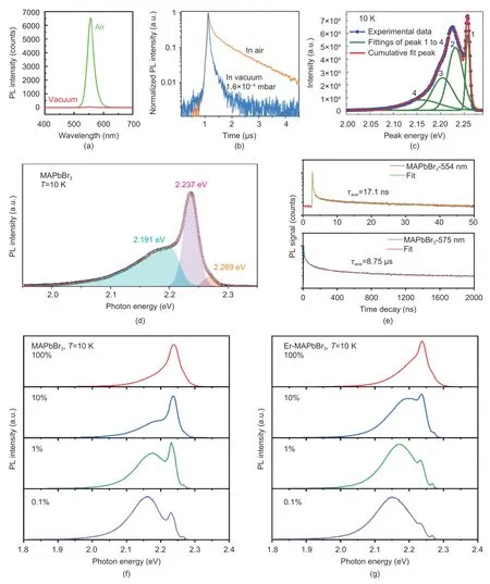
Fig.4.Optoelectronic properties of perovskite single crystals:Comparison of (a) PL spectra and (b) TRPL spectra of the MAPbBr3 single crystal under air and vacuum[38];(c) PL spectra of the MAPbBr3 single crystal fitted by the Gauss peak under 10 K[61];deconvolution of (d) PL spectra and (e) TRPL spectra of the MAPbBr3 single crystal[56];power-dependent PL of (f) MAPbBr3 and (g) Er-MAPbBr3 single crystals at 10 K[56].
3.3.Electronic Properties
Generally,the SCLC method is exploited to probe the electronic parameters like the conductivity,carrier mobility,and carrier diffusion length of single crystals[13],[20],[21].Actually,this method is utilized to measure the dark current-voltage (I-V) curve by fabricating the structure of metal/single-crystal wafer/metal (as illustrated inFig.5 (a)).The curve can be divided into three regions,including the Ohmic region,trap-filled region,and Child’s region.The conductivity can be calculated by the curve of the Ohmic region using the formula σ=I/(VL).The trap density can be determined by the following equation[21]:

where ε0is the vacuum permittivity,ε represents the relative permittivity,e is the elementary charge,L is the thickness of single-crystal wafers,and VTFLis the point between the Ohmic region and the trap-filled region as shown inFig.5 (a).The relative dielectric constant can be obtained from the capacitance-frequency measurement.Traps in single crystals act as dopants that influence the electronic properties,including the conductivity and carrier diffusion length.For thin films,the traps distribute on the surface,bulk,and near grain boundaries.However,there are almost no grain boundaries in single crystals,which indicates the traps are primarily distributed on the surface and bulk.As a result,there are fewer trap densities (≈1010cm–3) compared with thin films (≈1014cm–3to 1017cm–3)[65].The carrier mobility (μ) can be calculated according to Mott-Gurney’s law in the Child region (n=2),which was determined by the following equation[66]:
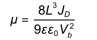
where JDis the current density and Vbrepresents the applied voltage.The carrier mobility represents the transmission rate per voltage of electrons and holes,which will be influenced by traps.Until now,the carrier mobility is about 150 ± 15 cm2V–1s–1for FAPbI3single crystals,and the SCLC curve is shown inFig.5 (a)[21].The carrier mobility is the highest,when fabricating MA0.45FA0.55PbI3(271 ± 60 cm2V–1s–1) single crystals[21](Fig.5 (b)).The Hall effect measurement is also useful to find the carrier mobility of single crystals,and for MAPbI3,the hole mobility (105 ± 35 cm2V–1s–1) measured by this method is almost corresponding to the result(164 ± 25 cm2V–1s–1) of the SCLC measurement.The diffusion length (LD) is also an important parameter which is determined by using the carrier mobility μ and carrier lifetime τ.The equation is given as follows:
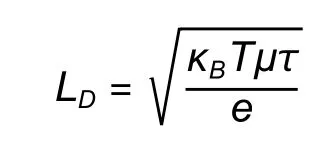
where κBrepresents the Boltzmann constant and T is the temperature.The carrier diffusion length for crystals ranges from 3 μm to 3 mm according to the previous report[67].Although,it is proven that the reported diffusion length exists with a certain deviation due to the contact resistance and high electric field.Lead sulfide (PbS) quantum dots (QDs) were used as quenchers to add into the MAPbBr3single crystals,and the relationship between the lifetime of the excited state and the quencher spacing can be determined by changing the density of the quencher.This method was exploited to measure the carrier mobility and lifetime,both of which determine the diffusion length of 2.6 μm in MAPbBr3single crystals[67],as illustrated inFigs.5 (c)and(d).For single crystals,the carrier lifetimes calculated by the TRPL spectra with twoexponential fitting exhibit fast and slow components which originate from surface and bulk traps,respectively.The TRPL spectra of MAPbI3and MAPbBr3single crystals show the lifetime of each component,as shown inFigs.5 (e)and(f)[17].The PL and electronic parameters are compiled inTable 1.
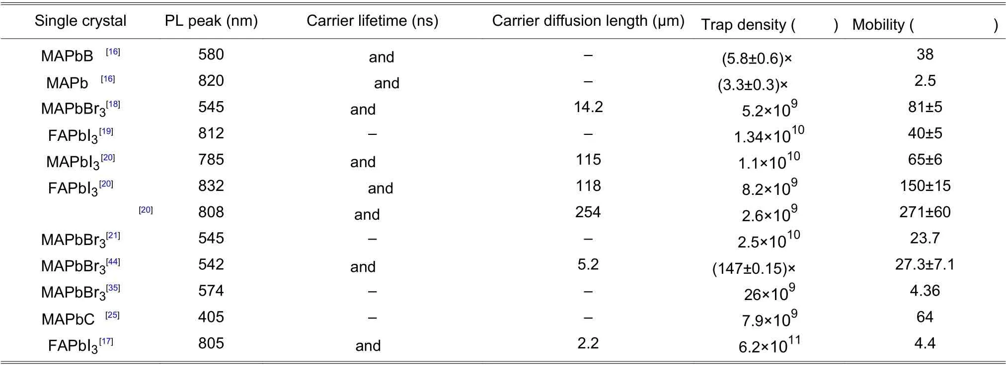
Table 1:Optoelectronic properties of perovskite single crystals reported in the literature

Fig.5.Electronic properties of perovskite single crystals:(a) SCLC curve of the FAPbI3 single crystal and device structure for measurement[21];(b) SCLC curve of the MA0.45FA0.55PbI3 single crystal which obtains high carrier mobility[21];(c) resulted carrier mobility by fitting diffusion coefficients[67];(d) lifetime and diffusion length based on MAPbBr3 single crystals by contactless measurement[67];TRPL spectra of (e) MAPbBr3 and (f) MAPbI3 single crystals[17].
4.Applications
Perovskite thin films with outstanding photovoltaic properties show advantages in applications,such as PDs[26],[27],[66],solar cells[9],[22],[68],lasers[29]-[31],and LEDs[30],[69].In contrast,single crystals have great potential due to the superior features.The architecture of single-crystal devices includes vertical and lateral structures.Among them,the latter overcomes the obstacles that the thickness of single crystals brings,and shows diverse applications.
4.1.Photodetectors (PDs)
Perovskite PDs can be implemented in camera imaging,communications,medical equipment,etc.,which can convert light signals to electronic signals.The responsivity (R) and EQE are basic parameters to evaluate PDs.R is a critical parameter that describes the response efficiency of optical to electronic signals,reflecting the efficiency of response to the optical signal.R is defined as the proportion of the photocurrent to the incident light intensity,which can be given as follows[19],[20],[28]:
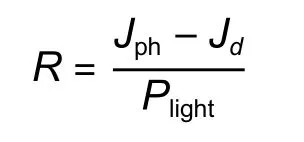
where Jphis the photocurrent,Jdis the dark current,and Plightis the incident light intensity.EQE is the value that transforms the photons to charge carriers (electrons and holes),given by the following equation[26],[66]:

where h is the Planck constant,c is the speed of light,and λ is the wavelength of incident light.Generally,EQE with a same trend as R is used as a figure of merit reflecting the collection efficiency of photo-generated charge carriers and is defined as the number of carriers that are circulated through PD for each incident photon.In tradition,the structure of PD is metal/electron transport layer (ETL)/perovskite/hole transport layer(HTL)/indium-tin oxide (ITO).Based on this structure,PD made of CsPbIBr2perovskite thin films showed a response of 21.5 pW/cm2and fast response time of 20 ns,which is the best perovskite thin-film device[70].While,this structure is not suitable for the single-crystal PD,because the thickness exceeds the carrier diffusion length,which will cause more carriers recombination.
The interdigital electrode with the gold (Au)/single crystal has been proposed,in which the device only uses a part near the surface to operate.PDs with this type of structure exhibit superior sensitivity.Lian et al.deposited Au on the (100) facet of the MAPbI3single crystal to fabricate planar-type PDs[66],as shown inFig.6 (a).The polycrystalline-film PD was also fabricated,asFigs.6 (b)and(c)exhibit that R and EQE of single-crystal PDs are at least 100 folds higher than film PDs and the response time is comparatively~1000 times faster,which is attributed to the low defect density of single crystals.Shen’s group synthesized transparent MAPbCl3PDs to detect UV light[28].The R spectra show a narrowband centered at 415 nm with high R of 3.73 A/W at 30 V,which pave the way to develop high-performance PDs.Moreover,alloyed MA0.45FA0.55PbI3single crystals that can be stored in air for at least 14 months were fabricated with verticalstructure PDs which show outstanding stability[21].PD based on MAPbBr3single crystals synthesized by LTGC was reported with R as high as 1.6 × 10⁴mA/W and EQE as large as 3900% (Figs.6 (d)to(f))[19].Meanwhile,it also shows excellent stability and the current only loses 10% after stored in air for 35 days.MAPbBr3singlecrystal PDs not only can detect visible light but also are sensitive to X-rays[41](Figs.6 (g)and(h)).It is demonstrated that the MAPbBr3single crystals show a high μτ product and low surface recombination velocity,which contribute to the sensitive X-ray detectors.The sensitivity for X-ray PDs can be achieved as high as 80 μC·Gyair–1cm–2,which is four times higher than α-Se detectors[71].This discovery may expand the applications of single-crystal PDs in the medical industry.

Fig.6.PDs based on perovskite single crystals:(a) schematics of the planar MAPbI3 single-crystal PD based on the (100)facet;(b) R and (c) EQE of single-crystal PD and thin-film PD under 532-nm laser at a fixed bias voltage of 1 V[66];(d) device structure of MAPbBr3 single-crystal PD;(e) current curves of PDs under the illumination with the intensity ranging from 3 mW/cm2 to 60 mW/cm2 at 525 nm;(f) EQE and detectivity (D*) spectra for PDs with the wavelength ranging from 325 nm to 650 nm at 4 V[19];(g) device structure of the sensitive X-ray detector;(h) transient current curves of MAPbBr3 single-crystal detectors under different bias[41];(i) response time of MAPbI3 single crystal PD under a light intensity of 1.8 mW/cm2 at 532 nm without external bias[78].
Recently,the self-powered PDs (that work without external bias) have grabbed huge attention,such as ZnO nanowires (NWs)/Au[72]and Ga2O3/Au[73]-[77].Part of perovskite single-crystal PDs also obtain a selfpowered feature which is driven by the strong built-in electric field.The built-in electric field can separate electron-hole pairs efficiently,which comes from the Schottky junction.Self-powered PDs make it possible to work under extreme conditions.MAPbI3single-crystal PDs with Al and Au integrated electrodes showed higher responsivity under a weak light intensity and rapid rise time of~70 μs without an external bias voltage(Fig.6 (i))[78].PDs based on MAPbBr3and MAPbIxBr3–xsingle crystals formed the perovskite heterojunction and obtained EQE of exceeding 3% which is about 15 times higher than those reported at zero bias[79].The visible-blind UV-PD based on MAPbCl3was recently reported to be synthesized through surface wettability engineering techniques and the space confined method.This UV-PD exhibited an ultrafast response speed of 15 ns and higher detectivity (6 × 10¹²J) while comparing with the inorganic semiconductor based visible-blind UV-PDs grown through traditional high-temperature fabrication routes.The response speed of this PD with different crystal thicknesses was determined through the transient photocurrent (TPC) measurement at zero bias (self-powered).The response time was found to be much faster than polycrystalline thin films and bulk single crystals based PDs;which is also the fastest reported to date[80].PDs (conventional and self-powered)based on perovskite single crystals are better in terms of their overall performance and operational stability compared with conventional polycrystalline based PDs.We foresee that cost-effective,solution-processible,and high-performance single-crystal PDs will be deployed in optical communications and ultrafast detection applications.
4.2.Solar Cells
PSCs have achieved enormous attention and great progress in the past decade.Low defects,suitable thickness,uniform films (large grain sizes,lesser grain boundaries,and absence of pinholes),etc.,are important factors to improve the quality of perovskite active layer absorbers for high-efficiency solar cells[3],[4],[81],[82].The basic parameters of solar cells include the open-circuit voltage (Voc),short-circuit current density (Jsc),FF,and power conversion efficiency (PCE).Metal halide single-crystal PSCs are promising for higher efficiency and improved stability,but their development lags far behind that of their polycrystalline counterparts.In particular,the low efficiency (<5%) of large-area devices makes the development of an alternative perovskite photovoltaic technology challenging.The thickness of perovskite thin films is generally~300 nm to 400 nm,which is limited by the diffusion length of the thin films (~100 nm)[83].Therefore,for single crystals,the thickness should match with the diffusion length which is at least several micrometers for fabricating high-performance solar cells[25].Metal halide single crystal based PSCs have attained the highest reported efficiency of 21.09% with just four years of research in this field regarding the specific device application[32].Theoretically,single-crystal perovskites,with their orders of magnitude lower defect density and higher carrier diffusion length compared with their polycrystalline counterparts,offer a chance for the PSC technology to overcome the limitation of polycrystalline thin films and get as close as practical to the Shockley-Queisser limit.Huang’s group reported the efficiency of solar cells with different thicknesses of crystal wafers through theoretical calculations[9].They designed PSC by replacing thin films to single crystals and obtained PCE of 16.1% through adjusting the thickness of crystal wafers.The single-crystal wafers were directly grown on the HTL substrate by a space confined method with varied thicknesses of crystal wafers.It can be found that the solar cells can get excellent I-V characteristics,when the thickness of wafer is 10 μm.It is indicated that larger defects exist on the surface compared with the bulk of crystals,which is caused by the loss of MAI[9].To reduce the defects on the surface,the MAI solution was additionally spin-coated on the crystal surface to get PCE of 17.8%,which is the best device of vertical-structure solar cells[9].
The carrier transport layer free device was reported through a facile and simpler fabrication structure[42].PSC based on this structure can lower the cost and reduce the loss of light that is induced by transparent carrier transport layers.The structure of the single-crystal solar cell was fabricated by depositing Au on one facet as the anode and gallium on the other facet as the cathode[13],as shown inFig.7 (a).If the single crystal is too thick,then the carriers cannot be efficiently extracted,as a result,the device performance is deteriorated.Therefore,the lateral-structure solar cells were proposed with the structure of metal/crystal,as shown inFig.7 (b)[60].PCE of the lateral-structure thin-film solar cell is generally below 0.1%,and comparatively single-crystal solar cells attain PCE of 1.88%[68].Recently the lateral-structure solar cell was reported to present high PCE of 11% with enhanced operational stability.The MAPbI3single crystal based solar cell was fabricated through a simple MAI treatment procedure.The MAI treatment significantly passivated surface defects,enhanced surface conductivity,and promoted the efficiency of the lateralstructure single-crystal perovskite solar cells (SC-PSCs).The excellent long-term operation stability of SCPSC was verified with no degradation after 200-hours continuous operation at the maximum power point(MPP) under 1-Sun illumination.With the development of large-area thin single crystals growth and surface passivation technique,it will show a bright future and potential towards efficient perovskite monocrystalline solar cells with dramatically reduced material and fabrication costs[84].Nevertheless,the devices based on single crystals show a strong piezoelectric effect,i.e.,the carriers are generated on squeezing the device.Fig.7 (c)represents the current density of lateral solar cells under the voltage ranging from 0 to 1 V[68].The J-V hysteresis and stability are major challenges with thin-film PSCs.Most recently,MAPbI3single-crystal PSC was fabricated with an active layer (MAPbI3) having a 20-μm thickness directly grown on a chargeselective contact through the solution space-limited inverse-temperature crystal growth method.The fabricated PSC device yielded the champion efficiency of about 21.09% and FF of up to 84.3%.The aforesaid PSC devices set a new record for single-crystal solar cells and opened up a new route to achieving high FFs in PSCs.The corresponding device geometry with relevant energy levels is represented as schematics inFig.7 (d)and the J-V curves with other PSC parameters are shown inFig.7 (e).Jscand PCE were also found at a bias voltage of 0.93 V as shown inFig.7 (f),which are outclassed among the corresponding devices[32].Moreover,solar cells based on MAPbBr3single crystals show outstanding stability with the PCE loss of about 7% in 1000 hours[22].The fabrication of single-crystal PSCs with potentially higher efficiency and enhanced stability is still in its initial stage.The reduction in the crystal thickness of perovskite single crystals is the Achilles heel for this technology but the control over this problem can fill the perforation between the carrier diffusion length and crystal thickness.For the upcoming development of single-crystal PSCs,the mechanism investigation based on small-area devices and the application exploration based on large-area devices should be conducted in parallel.The single-crystal PSCs have potential to replace the conventional thin-film photovoltaic technology if efficient large-area devices can be fabricated in near future.
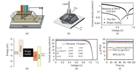
Fig.7.Solar cells based on perovskite single crystals:(a) vertical structure device architecture of PSC based on the MAPbI3 single crystal[13];(b) schematics of lateral structure solar cells[60];(c) J-V curves of devices based on MAPbI3 single crystals under 25-mW/cm2 illumination[68];(d) device-schematics for MAPbI3 single-crystal PSC denoting the energy levels of corresponding layers;(e) J-V curves of the champion cell in forward-scan (orange) and reverse-scan (blue) modes and the corresponding photovoltaic parameters under 1-Sun illumination;(f) steady-state photocurrent and PCE output at the maximum power point with 0.93-V bias for the champion cell[32].
4.3.Light Emitting Diodes (LEDs)
The electroluminescence (EL) property of perovskite semiconductors was first demonstrated in 1994 by Era et al.,but the process can only be operated in liquid-nitrogen temperature[85].Therefore,a high-quality perovskite layer is essential for fabricating efficient LEDs.Until 2014,Tan et al.prepared perovskite LEDs based on MAPbBr3thin films found at the green range,as well as MAPbIxCl1–xfound at the infrared range which are operational at room temperature instead of air[86].Whereas,this still creates stumbling blocks for applications.Perovskite single-crystalline MAPbBr3nanoplates produced by the modified ligand-assisted precipitation method show enhanced moisture resistance caused by hydrophobicity at the end of the long chains,bringing promise for LED devices.The nanoplates can be made stable for at least one week in air,which eliminates complex procedures of device preparation.Fig.8 (a)represents the structure and energy diagram of perovskite light emitting diodes (PeLEDs)[73].PeLEDs can emit bright green light at 530 nm with an intensity as high as 10590 cd/cm2and the current density as large as 874 mA/cm2,as illustrated inFigs.8 (b)and(c)[73],[87].
PeLEDs exhibit high color purity,broadband color tenability,and high charge-carrier mobility[69],[88],but the only drawback is low PL.Large-scale all-inorganic perovskite nanocrystals show highly efficient PL and visible shift of emission peaks[89].Except for PL,PeLEDs based on 2D (PEA)2PbBr4nanoplates not only exhibit PL but also show violet EL[90],whose peaks are close and centered at~410 nm.CsPbBr3nanoplates were directly grown onto the ITO electrodes by vapor-phase deposition to fabricate PeLEDs which obtain nice PL and EL properties[91],as shown inFig.8 (d).The PL peak intensity,in response to the EL intensity at 8 V,shows that the mechanism of luminescence is originated from the band-to-band emission.Otherwise,the simple structure ITO/p-type device provides a way for PeLEDs development.
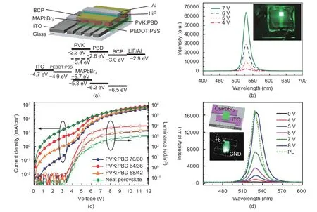
Fig.8.LEDs based on perovskite single crystals:(a) schematics of LED based on perovskite nanoplates and the flat-band energy level diagram of the device[73];(b) EL spectra of PeLED under various voltages (4 V to 7 V)[73];(c) J-V and luminescence of the device with various molar ratios of PVK (perovskite):PBD (poly(9-vinylcarbazole):2-(4-biphenylyl)-5-phenyl-1,3,4-oxadiazole)[87];(d) EL and PL (dashed line) spectra of PeLEDs fabricated by CsPbBr3 nanoplates[91].
4.4.Lasers
The lasers based on perovskite semiconductors show low amplified spontaneous emission (ASE) due to the outstanding characteristics[30],including large absorption coefficients,tunable emission wavelength peaks,low trap densities,and low Auger recombination.In contrast to 3D perovskite thin films,nanoparticles,nanoplates,and nanocrystals form a natural resonant cavity to achieve population inversion required for ASE and lasing.Lasers fabricated by perovskite single crystals have garnered huge attention of researchers as they show outstanding performance,including optical-gain media,spectrally narrow gain profiles,high quality factors,and low lasing thresholds.
Most of the perovskite lasers use the Whispering-gallery-mode (WGM) cavity[92],which is induced by internal reflections on the circumference of a circular or polygonal resonator in which the guided optical mode provides feedback.A spherical WGM laser was realized through coating perovskite materials on glass microspheres by atomic laser deposition (ALD),this manufacturing method is of great significance to the field of silicon photonics.Planar WGM lasers based on perovskite nanoplates were investigated.WGM MAPbI3lasers synthesized with chemical vapor deposition (CVD) and solution treatment show lasing thresholds of 37 μJ/cm2and 3.6 μJ/cm2[81],respectively.Near-infrared WGM MAPbI3nanoplates lasers exhibit high optical gain and tunable optical modes,and become the candidates to be integrated with Si technologies[93].As shown inFig.9 (a),clear diffraction patterns can be seen inside the WGM cavity under the illumination of white light and incident lasers,which indicates good optical confinement from the nanoplatelet WGM cavities[93].Fig.9 (b)shows the emission spectra around the lasing thresholds,it is obvious that the peaks blue-shifted with increasing the lasing intensity,which may be attributed to the change of the band filling mode or refractive index[93].Song’s group prepared MAPbBr3micro-rods lasers with the smallest full width at half maximum (FWHM) of 0.1 nm and Q exceeding 5000[80].The lasing thresholds of single-crystalline NWs are lower than the value of colloidal nanoplates,colloidal quantum dots (CQDs),and organic polymer lasers.Single-crystal MAPbBr3NWs based lasers put on the SiO2substrate pumped by 402-nm laser excitation,as shown inFig.9 (c)[29].The NW lasers achieved the lowest lasing threshold (220 nJ/cm2) and the highest Q factor(~3600) which are ascribed to the long lifetime and low non-radiation recombination (Fig.9 (d))[29].
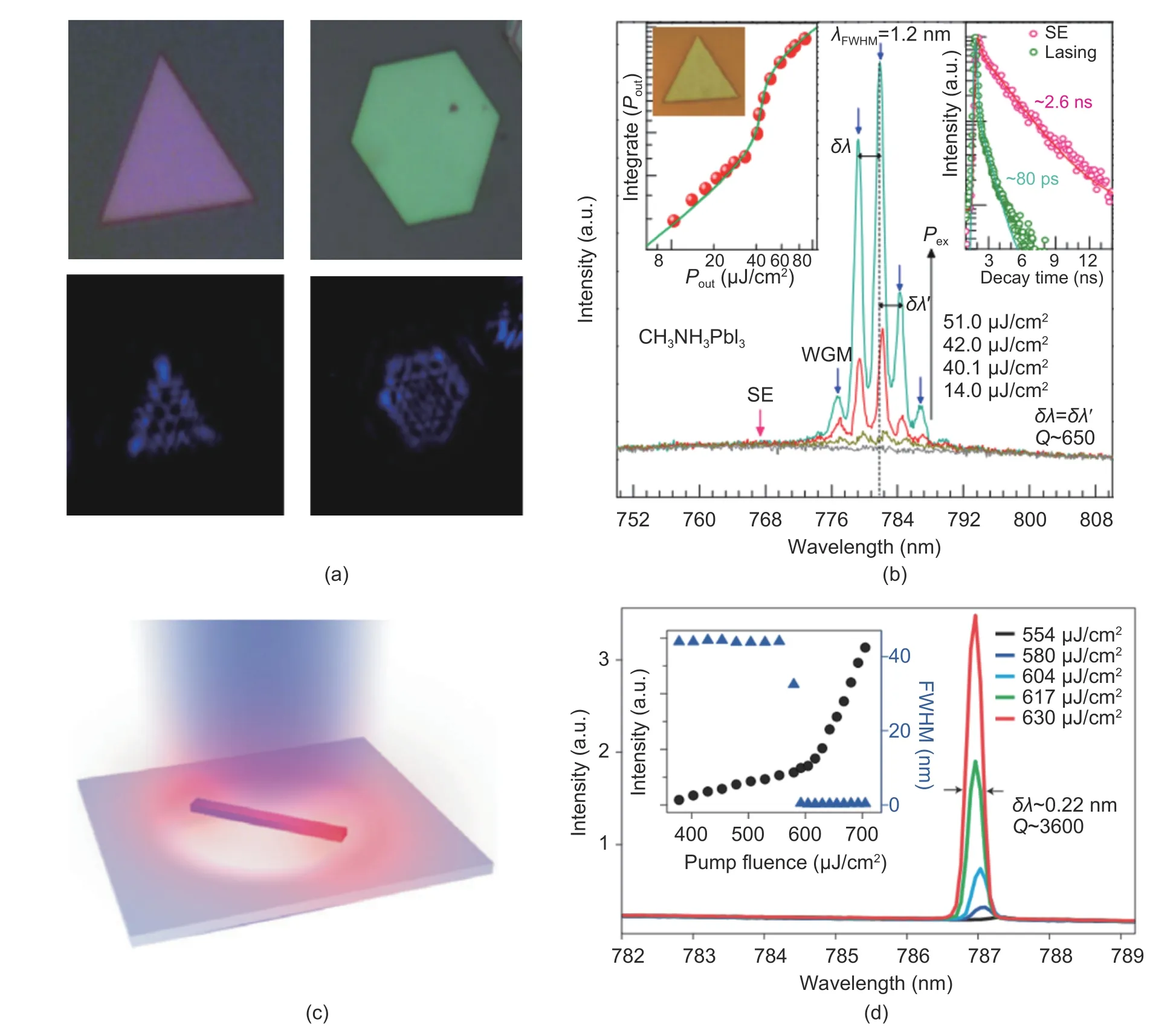
Fig.9.Lasers based on perovskite single crystals:(a) optical images of lasers based on MAPbI3 nanoplates under the white light and incident laser[93];(b) evolution from spontaneous emission to lasing in a typical MAPbI3 triangular nanoplate[93];(c) device architecture of NW on the SiO2 substrate pumped by 402-nm laser excitation[29];(d) emission spectra of lasers around the lasing threshold[29].
5.Summary and Outlooks
In this review,we summarized the growth and crystallization,properties,and applications of perovskite single crystals.The solubility of precursors in different solvents and methods to grow high-quality perovskite single crystals has been recapitulated to be dependent upon the temperature variations.Various synthesis methods as the AVC,STL,ITC,and electronic dynamic gradient (EDG) methods are effective and mature ways to fabricate high-quality single crystals with the thickness of several millimeters that are favorable for different applications.Generally,the carrier diffusion length of single crystals ranges from a few to several hundred microns,but the thickness of single crystals exceeds the diffusion length,which influences the effective carrier extraction.Until now,the two reported elucidations to avoid the thickness effects include:1) Perovskite single-crystal wafers (~10 μm) should be prepared;2) lateral device should be developed.
Although there are fewer traps in perovskite single crystals compared with thin films,the traps in crystals also influence the performance,especially the surface traps.Bandgap engineering is found to be an effective way to address the surface defects and to tune the desired bandgap.Two or three components can be substituted/doped at each site in the structure of ABX3.This method has the capacity to prepare non-toxic single crystals by replacing Pb at the B site with Sn,Bi,etc.Temperature-dependent PL and powerdependent PL exhibit the intrinsic features of single crystals,which is attributed to the high purity compared with thin films.It provides indications to reduce traps and to explore the application environment.Implementing high-quality perovskite single crystals into demanding applications,like LEDs,PDs,and solar cells,not only improves the performance of these devices but also simplifies their structures and offers ease of fabrication through diverse methods.Therefore,besides careful optimization of bulk-crystal quality improvement,the development of rational surface passivation techniques is urgently needed.The interdependence of the structure and property in single-crystalline perovskite films is yet to be established to enrich the high-speed photon detection applications.Regarding the challenges in device applications,the narrower bandgap,higher exciton concentration with less recombination,and highly efficient carrier extraction are key factors for highly efficient single-crystalline based photovoltaics.The specific property of carrier multiplication within perovskite single crystals needs further exploration and optimization to provide a higher density of effective carriers contributing to the overall device performance.Therefore,future outlook for perovskite single-crystal applications is as follows:1) B-site substitutional doping of various elements should be opted to improve optoelectronic properties of single crystals,with the adjustment of doping levels so as to reduce the Ohmic losses during charge carrier collection at mean,and to avoid the crystals to exhibit purely metallic behavior at extreme;2) crystals should be grown directly on the substrate to reduce the energy barrier between two layers,and intensive consideration is required to minimize the lattice mismatch,to evade interfacial losses;3) special care must be taken to design novel device structures and to organize effective electronic contacts between the interfaces,to minimize the defects and traps;4) the lateral device geometry to be opted for better morphologies and electrical properties leads to the enhanced efficiency and stability of these devices in industrial applications.
Synthesis control over the orientation and thickness of large-area single-crystal films is required to put this technology a step ahead regarding their integration into the aforesaid photovoltaic devices.Strategies must be developed and challenges must be addressed in replacing the unstable MA cation and toxic Pb,to yield Pb-free all-inorganic perovskites,which can pave the way for ambient stable devices.Thin 2D perovskite single crystals have benefits of their structural relaxations and enhanced PL intensities,so it can be best for LEDs.Regarding to the device fabrication and control,the quasi 2D and mixed 2D/3D perovskites with Lewis base surface treatments are promising candidates.The 2D/3D mixed perovskite single crystals with the possible optimizations can be employed into single-junction and multi-junction devices with enhanced stability.Most of the perovskite materials utilized for single crystals are mainly the organic-inorganic hybrid perovskites like MAPbBr3and MAPbI3.Because of the instability of the volatile organic moiety and Pb toxicity issues,all-inorganic and Pb-free perovskite compositions having low toxicity can be good for future prospect of single crystals synthesis techniques and applications.
Disclosures
The authors declare no conflicts of interest.
 Journal of Electronic Science and Technology2021年2期
- Journal of Electronic Science and Technology的其它文章
- Progress and Prospects of Hydrogen Production:Opportunities and Challenges
- Improved Active Islanding Detection Technique for Multi-Inverter Power System
- Big Data-Based Transformer Substation Fault Prediction Method
- Comparison of Khasi Speech Representations with Different Spectral Features and Hidden Markov States
- Neural Network Based Adaptive Tracking of Nonlinear Multi-Agent System
