Fabrication and characterization of Al-Mn superconducting films for applications in TES bolometers*
Qing Yu(余晴) Yi-Fei Zhang(张翼飞) Chang-Hao Zhao(赵昌昊) Kai-Yong He(何楷泳)Ru-Tian Huang(黄汝田) Yong-Cheng He(何永成) Xin-Yu Wu(吴歆宇)Jian-She Liu(刘建设) and Wei Chen(陈炜)
1Department of Microelectronics and Nanoelectronics,Tsinghua University,Beijing 100084,China
2Beijing National Research Center for Information Science and Technology,Beijing 100084,China
3Institute of High Energy Physics,Chinese Academy of Sciences,Beijing 100049,China
4Tsinghua University Future Chip Technology Advanced Innovation Center,Beijing 100084,China
Keywords: Al-Mn superconducting films,deposition process,annealing process,superconducting transition edge sensor
1. Introduction
Superconducting transition edge sensor (TES) detectors are widely used as bolometers or micro calorimeters that adopt superconducting thin films as thermometers.[1]Owing to the excellent sensitivity, great noise performance, rapid response and good response linearity,TES has become a popular technique of detecting submillimeter microwave, optical, and xray signals.[2,3]One major application of TES bolometers is to detect the B-mode polarization signature of cosmic microwave background(CMB)due to gravitational lensing. The observation site where TES bolometers are deployed for actual astronomical detecting needs to be in high-altitude to ensure crucial dry environmental condition. Only four places on the earth are suitable for CMB observations,which are the South Pole, Atacama Desert in northern Chile, Greenland, and Ali in Tibet,China. Several groups have deployed CMB detecting telescope system such as background imaging of cosmic extragalactic polarization(BICEP)[4,5]and south pole telescope(SPT)[6,7]at the South Pole, atacama cosmology telescope(ACT)[8,9]and POLARBEAR[10]in Chile, and AliCPT[11](Ali CMB polarization telescope(AliCPT)[11]in Tibet,China.The design of TES bolometers for B-mode signal detecting integrates antenna, bandpass filter and TES bolometer island.We have completed the entire TES bolometer design, and we will describe the related methods and results in the subsequent reports. In this paper,we introduce the fabrication and characterization of Al-Mn superconducting films, which is the key component on TES bolometer island.
The critical temperatureTcand superconducting transition width ΔTcof superconducting film is crucial to device performance.The choice ofTcis a compromise between the noise performance and the base temperature in refrigerator. The value of ΔTcdetermines the thermal sensitivity parameter[1]

whose larger value represents sharper transition. The value ofαaffects the response speed and sensitivity of TES bolometer.In our TES bolometers, the value ofTcand ΔTcare designed to be around 540 mK and 1.0 mK respectively. In the BICEP experiments chosen are a Ti film with a critical temperatureTcof 400 mK for cosmic experiments and an Al film withTcof 1.1 K for laboratory calibration.[4]In the SPT experiments the Mo-Au bi-layer films are used[7]while in POLARBEAR projects the Al-Ti bi-layer films are adopted.[10]Compared with elementary films,superconducting-normal metal bi-layer films can achieve adjustableTccontrolled by thickness of superconducting film and normal metal film based on the principle of mutual proximity effect.[12-16]The normal metals in bi-layer film are usually very thin (~50 nm) and difficult to control precisely in fabrication,leading to the instability in superconducting properties. Magnetic ion doping in elemental superconducting film is another method to controlTc. Compared with the bi-layer films,alloy films avoid the complicated mutual proximity effects and resulting films are more stable.The manufacturing of alloy films is easy with DC-magnetron sputtering process. TheTcof Al can be suppressed significantly with minor Mn doping as reported in Refs. [17-21].The ACT projects have suppressed theTcof Al from~1.1 K to~200 mK with Mn concentration in the 2000-ppm regime by atomic percentage,[8]they also carried out a series of experiments to explore the annealing process of Al-Mn alloy film. The suppression ofTcby magnetic ion doping is generally elucidated by Abrikosov-Gor’kov model,[22]which proposes that cooper pairs are affected by the exchange interaction between electrons and spinning impurity atoms. But according to the strong suppression ofTcin Al-Mn alloy films,Friedel-Anderson model[23]is more suitable that emphasizes pair scattering from resonant magnetic impurity sites,which is quantified by the Kaiser theory.[24]
We explore the deposition processes of Al-Mn films including sputtering pressure and annealing process. TheTcand ΔTcof deposited superconducting films are characterized and optimized. We successfully fabricate Al-Mn films withTcaround 540 mK and ΔTcbelow 1.0 mK with Mn concentration of 1200 ppm in Al target.
2. Method
The deposition system is CMS-18 UHV sputtering deposition system from Kurt J. Lesker company. This equipment is used for depositing the Al-Mn films exclusively to avoid being contaminated and can ensure an ultra-high base vacuum of 3×10⁻⁹Torr(1 Torr=1.33322×10²Pa). The sputtering chamber is configured with three DC-magnetron sputtering sources that can accommodate 3-inch (1 inch=2.54 cm)targets. The parameters of deposition processes are listed in Table 1. To measure the actual temperature of wafer during the sputtering process,we attached temperature monitoring labels besides the sample.The temperatures shown by the labels were always below 60°C for a 3000-s-sputtering test.
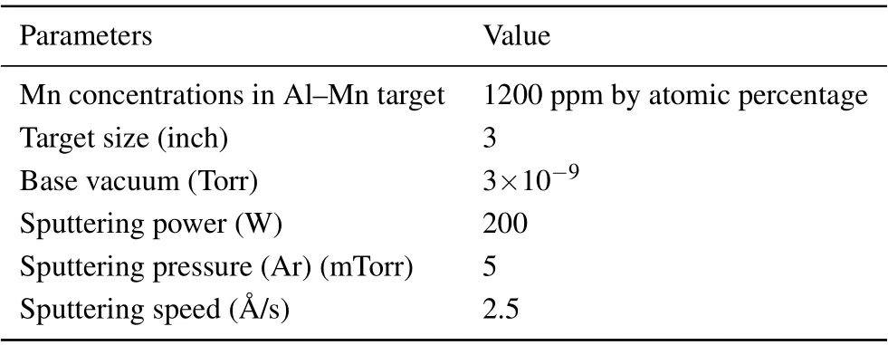
Table 1. Parameters of deposition process.
The substrate was a silicon wafer with a 1.0-μm-thick low-stress silicon nitride film grown on its top. The deposited samples had different Mn concentrations. The samples with 1200-ppm Mn concentration were cooled by a He-3 refrigerator with a base temperature of 335 mK. The He-3 refrigerator was equipped with 64 DC wires (Mn-Cu alloy twisted pairs) from mK range to room temperature. Schematic diagram of electric connection is shown in Fig.1(a). TheTcvalues of films with 2000-ppm Mn concentration were between 100 mK-200 mK,and these samples were cooled by a dilution refrigerator,which could reach a base temperature of 50 mK.The electrical resistance values of films were measured using the four-terminal method[25]with a DC current source in I terminals and voltage read out between V terminals as illustrated in Fig.1(b).
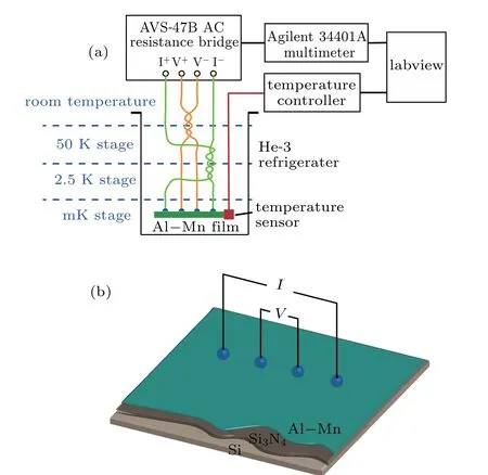
Fig.1. Schematic diagram of R-T measurement set-up of Al-Mn films. (a)Schematic diagram of electric connection. Samples are cooled by He-3 refrigerator. AVS-47B bridge is used to read out film resistance, which can provide μA-level current to test low temperature resistance accurately. Agilent 34401A digital multimeter is used to transform analog signals into digital signals. A temperature sensor and a temperature controller are used to monitor actual temperature of film. (b)Electrical resistance of film is measured using four-terminal method with a DC current source in I terminals and voltage sensor between V terminals.Substrate is silicon wafer with 1.0-μm-thick silicon nitride layer grown on the top.
3. Results and discussion
We study the effect of thickness of film on superconductivity as shown in Figs. 2(a) and 2(b). Films with thickness varying from 50 nm to 300 nm,are deposited on seven wafers.The deposition parameters are listed in Table 1. From theR-Tcurves, it can be observed that both the square resistanceRsqandTcdecrease as the thickness increases, which is in contrast to the scenarios of most elemental[26]and compound superconducting films,[27,28]but similar to behaviors of pure Al films.[29,30]Figure 2(b)indicates that the value of ΔTcis below 1.0 mK for thickness between 70 nm and 300 nm.
The Al-Mn films are deposited under different sputtering pressures ranging from 1 mTorr to 15 mTorr. The thickness is controlled at 150 nm(±10 nm). The other deposition parameters are the same as those listed in Table 1. Figure 3 shows the sputtering pressure dependence ofTcand ΔTcobserved inRTcurves. There occurs a minimum ΔTcof 0.7 mK at pressure around 8 mTorr.
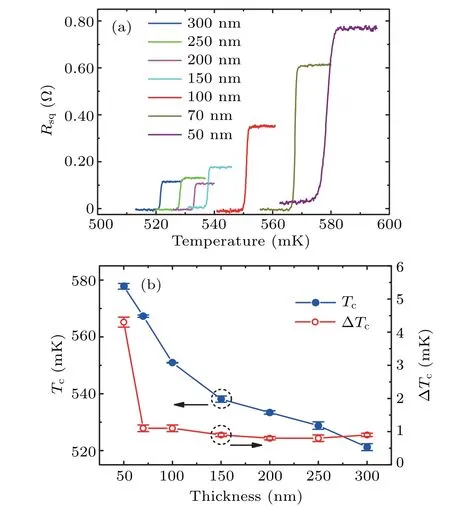
Fig. 2. (a) R-T characteristics of Al-Mn films of different thicknesses; (b)thickness dependence of Tc and ΔTc observed in R-T curves,where each data point is an average of several measurements and error bars are also shown.
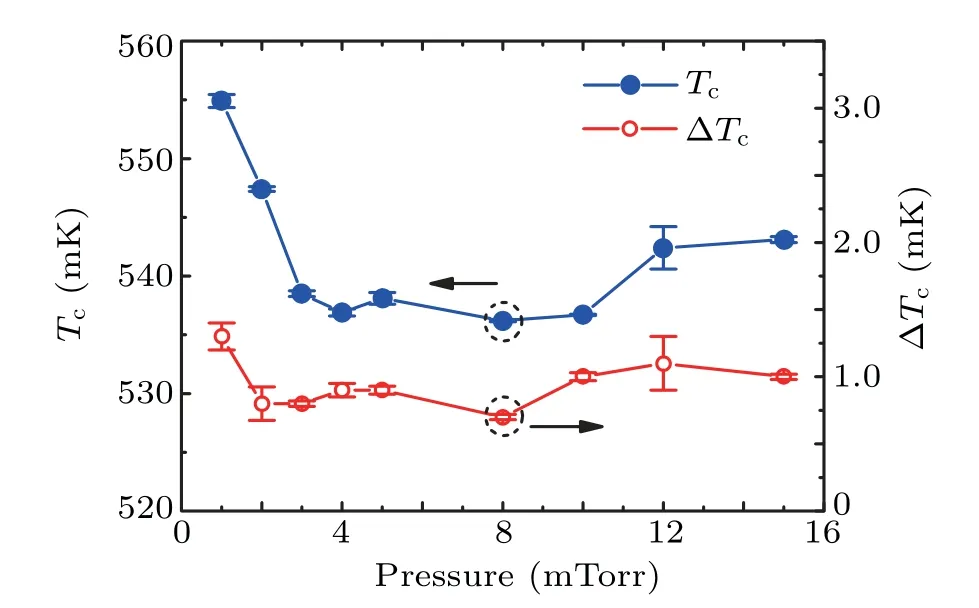
Fig. 3. Sputtering pressure dependence of Tc and ΔTc observed in R-T curves, where sputtering pressure varies from 1 mTorr to 15 mTorr. Thickness is controlled at 150 nm(±10 nm). Other deposition parameters are the same as listed in Table 1. Data point and error bars are obtained by averaging several measurements of the same sample.
In the photolithography process of the microfabrication of TES, it is common to bake the wafers to remove moisture or to harden the photoresist. The influence of annealing process on superconducting properties ought to be verified. The wafers are cut into pieces and annealed on a hot plate at temperatures from 90°C to 330°C for 10 min. The changes ofTcand ΔTcare shown in Figs.4(a)and 4(b),indicating the results of annealing in 1200-ppm and 2000-ppm Mn concentrations,respectively. When films are baked at 120°C in 1200-ppm concentration regime, theTcvalue drops from the 540 mK to~400 mK.As the annealing temperature increases to 330°C,Tcthen reaches 640 mK. And for films annealed in a 2000-ppm concentration, theTcvalue drops from the~190 mK to~130 mK at 120-°C baking temperature, and then increases to 400 mK at 330-°C baking temperature as illustrated in Fig.4(b). The change trend ofTcvalue is in consistent with that in the literature.[8]When the baking temperature reaches 300°C,the value of ΔTcis higher than 4.0 mK,indicating that the superconducting properties start to become worse. Hence it is necessary to avoid heating the substrate to an excessively high temperature in fabrication process. Annealing treatment has a great influence onTcand ΔTc, due possibly to the recrystallization behavior,the change of Mn distribution and the transform of mechanical stress properties, which needs to be studied further. To verify the process repeatability,two wafers with different doping concentrations are deposited and baked. The difference inTcvalue between the two wafers is within 50 mK,which may be due to the minor heating uniformity.
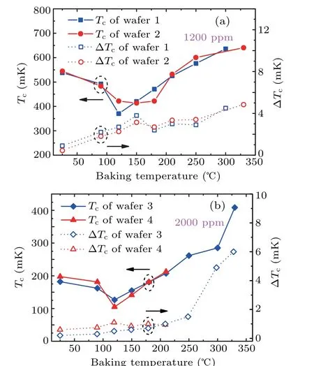
Fig.4. Curves of Tc and ΔTc versus annealing temperature,where(a)wafer 1 and wafer 2 are deposited with 1200-ppm Mn doping concentration, with deposition parameters shown in Table 1 and deposited layer thickness being 150 nm (±10 nm), and (b) wafer 3 and wafer 4 are deposited with 2000-ppm Mn doping concentration,with deposition power being 200 W,pressure being 5 mTorr,and deposited layer thickness being 240 nm(±10 nm).
4. Conclusions
In this work, we have studied the effect of deposition and annealing process on superconducting properties of Al-Mn films for their applications in TES bolometers. TunableTcis accomplished by varying thickness of film or by annealing. The value of ΔTccan be steadily controlled below 1.0 mK to guarantee a sharp normal-to-superconductor transition. The superconducting properties deteriorate by annealing at an excessively high temperature.
Acknowledgement
The authors thank Zhengwei Li for his great help in the deposition experiments.
- Chinese Physics B的其它文章
- Projective representation of D6 group in twisted bilayer graphene*
- Bilayer twisting as a mean to isolate connected flat bands in a kagome lattice through Wigner crystallization*
- Magnon bands in twisted bilayer honeycomb quantum magnets*
- Faraday rotations,ellipticity,and circular dichroism in magneto-optical spectrum of moir´e superlattices*
- Nonlocal advantage of quantum coherence and entanglement of two spins under intrinsic decoherence*
- Universal quantum control based on parametric modulation in superconducting circuits*

