High-responsivity solar-blind photodetector based on MOCVD-grown Si-doped β-Ga2O3 thin film*
Yu-Song Zhi(支钰崧), Wei-Yu Jiang(江为宇), Zeng Liu(刘增),5, Yuan-Yuan Liu(刘媛媛),Xu-Long Chu(褚旭龙),4, Jia-Hang Liu(刘佳航), Shan Li(李山), Zu-Yong Yan(晏祖勇),Yue-Hui Wang(王月晖), Pei-Gang Li(李培刚),†, Zhen-Ping Wu(吴真平), and Wei-Hua Tang(唐为华),5,‡
1Laboratory of Information Functional Materials and Devices,School of Science&State Key Laboratory of Information Photonics and Optical Communications,Beijing University of Posts and Telecommunications,Beijing 100876,China
2Center of Materials Science and Optoelectronics Engineering,University of Chinese Academy of Sciences,Beijing 100049,China
3The Engineering Research Center for Semiconductor Integrated Technology,Institute of Semiconductors,Chinese Academy of Sciences,Beijing 100083,China
4China Aerospace System Simulation Technology Co.,Ltd. (Beijing),Beijing 100195,China
5College of Electronic and Optical Engineering&College of Microelectronics,Nanjing University of Posts and Telecommunications,Nanjing 210023,China
Keywords: Si-doped β-Ga2O3,metal-organic chemical vapor deposition(MOCVD),solar-blind,high responsivity
1. Introduction
Since ultraviolet (UV) radiation was discovered by Johann Ritter in 1801, it has received extensive research for its influence on the survival and development of humankind.[1,2]According to the International Commission on Illumination,the ultraviolet spectrum could be divided into three bands:UVA, UVB, and UVC.[3]Due to the strong absorption of the protective ozone layer, the UVC region is also called as the solar-blind region, which means the noise signal of the UVC radiation in natural background is very weak and the radiation signal could be very accurately detected.[4]Thus, solar-blind photodetectors (PDs) have plenty of applications in flame sensing, information communication, chemical/biological analysis, etc.[5,6]Among various solar-blind photodetectors, Ga2O3is deemed as a promising candidate for UVC detection because of its proper bandgap(~4.9 eV),good reliability,and availability.[7,8]Up to now,various kinds of Ga2O3based PDs are extensively investigated.[9]Metal–semiconductor–metal(MSM)structured devices are fabricated on β, α, and ε phase Ga2O3films to study their photodetective abilities.[10–14]Schottky junction, heterojunction,and van der walls junction between various materials and Ga2O3films are also exploited to explore the relevant photoconductive and photovoltaic properties.[15–21]Metal–oxide–semiconductor field effect transistor structured Ga2O3PDs are also fabricated to investigate their behaviors as solar-blind phototransistors.[22,23]In addition, as the defects and doped elements affect the carrier transport properties significantly,doping could also be an effective way to enhance the performance of PDs.[24–26]For instance,Zhao et al. investigated the photoelectric characteristics of Sn-doped Ga2O3.[27]Kokubun et al.[28]and Tian et al.[29]studied the behaviors of In-doped Ga2O3based photodetector. Grundmann et al. demonstrated UV PDs based on a Si-doped(InxGa1−x)2O3thin film by PLD methods.[30]Cui et al.[31]and Wuu et al.[32]investigated the photodetector characteristics of Al-doped Ga2O3. Zhao et al.[33]and Alema et al.[34]observed the improved photoelectric performance in Zn-doped β-Ga2O3films. Guo et al. investigated the Mg-doped p-type β-Ga2O3thin film for solarblind ultraviolet photodetector.[35]Moreover,Fang et al. fabricated high quality p-type β-Ga2O3films by doping N elements and paved a novel way to fabricate super sensitive oxide semiconductor photodetectors.[36]However, although doping Si elements is as an effective way to enhance the conductivity of Ga2O3,reports about Si-doped Ga2O3PDs are limited.Currently, Kim et al.[37]and Pearton et al.[38]have studied the photoresponse properties of the Si-implanted Ga2O3. The metalorganic chemical vapor deposition (MOCVD) is an effective way to deposit Si-doped Ga2O3films.[39]More investigation about the Si-doped Ga2O3PDs is still required.
Thus,in this paper,Si-doped Ga2O3films were deposited on sapphire substrate by MOCVD methods. An MSM structured PDs device was fabricated and the electric behaviors of the device were measured under dark and 254 nm illumination. With I–V and I–t measurements,the results indicate that Si-doped Ga2O3films have great potential in solar-blind photodetector fields.
2. Experimental details
Si-doped Ga2O3films were deposited on (0 0 0 1) sapphire substrate by MOCVD methods and obtained from Beijing Gallium Family Technology Co., Ltd. Triethylgallium(TEGa), tetraethyl orthosilicate (TEOS), and high purity O2were used as metalorganic precursors for Ga elements, Si elements,and oxidation,respectively,while high purity Ar was used as the carrier gas. During the deposition, the flow rates of the TEGa and TEOS were fixed at 490 sccm and 15 sccm,respectively. The pressure of the chamber was kept at 25 Torr and the deposition temperature was set at 590°C.
To characterize the crystal structure of the deposited films, x-ray diffraction (XRD) was executed by a Bruker D8 Advance x-ray diffractometer with Cu Kα (λ ~1.5405 ˚A)radiation. Furthermore, the element contents of the deposited films were analyzed by secondary ion mass spectrometry(SIMS,TOF-SIMS,IONTOF 5)and x-ray photoelectron spectroscopy(XPS)measurements(ESCALAB 250Xi, ThermoFisher Scientific). Moreover, ultraviolet visible (UV-vis)absorption spectrum was utilized to investigate the absorbance and calculate the optical bandgap of the Si-doped Ga2O3films.Spectroscopic ellipsometry (SE) (SE-VE, Eoptics) was performed to estimate the thickness of the deposited films, and the ellipsometry measurement was performed with a wavelength ranging from 400 nm to 800 nm at an incidence angle of 65°. To further study the photoelectric behavior of the deposited films,an interdigital Ti/Au electrode was grown on the Si-doped Ga2O3films through standard photolithography,magnetron sputtering deposition, and lift-off process successively. As shown in Fig. 4(a), the interdigital electrode was composed of 54 pairs of electrode fingers, and the length,width, and space gap of the electrode fingers were designed as 3300 µm, 10 µm, and 20 µm, respectively. The Ti/Au electrode was grown by magnetron sputtering and the thickness of Ti/Au was around 20 nm/70 nm. After the device was fabricated,Keithley 4200 semiconductor characterization system was employed to investigate the electric and photoelectric properties, while a UV lamp was placed over the device to provide 254 nm illumination.
3. Results and discussion
As shown in Fig. 1(a), Si-doped Ga2O3films grown on(0001) Al2O3substrates have a monoclinic β phase crystal structure as determined by XRD θ–2θ scan (JCPDS card No. 43-1012). In addition to the diffraction peak of the sapphire substrate, three main peaks located at around 18.90°,38.32°, 59.0°are observed and can be assigned as (¯2 0 1),(¯4 0 2), (¯6 0 3)planes of β-Ga2O3.[40]Moreover, peaks with relatively low intensity are found at around 44.59°and 60.4°,which can be ascribed to the(¯6 0 1)and(¯8 0 1)planes of β-Ga2O3,indicating that the films grown by MOCVD under this deposition condition mainly are poly-crystalline with the doping of Si elements.Figure 1(b)displays the UV-vis absorbance of the Si-doped Ga2O3films.From the profiles,it can be found that the sample shows a significant absorption edge at around 268 nm while exhibiting no obvious absorbance in UV-B,UVA, and visible regions. Hence, (αhν)2is plotted against the photon energy(hν)in the inset and the optical band gap is extracted to be 4.75 eV by fitting the linear region. The results imply that the doped Si element does not significantly change the absorption edge and the optical band gap of the Ga2O3films. Moreover,XPS and SIMS measurements were utilized to further identify the chemical components of the films. Before analyzing the XPS results, the charge shift spectrum is calibrated through the core level energy of C 1s from the surface absorbate.

Fig. 1. (a) XRD scan and (b) UV-vis absorbance spectrum of the deposited Si-doped Ga2O3 films. The corresponding plot of(αhν)2 versus hν for the sample is shown in the inset.
To find of the Si signal in XPS spectra, a fine scan was carried out in the range of 90–173 eV with a measuring step of 0.05 eV,and the results are displayed in Fig.2(a).As shown in this figure, the black line-symbol plot represents the original measured data,while the red line and the green line represent the fitting curve and the background, respectively. From the fitting curve,it can be found that the XPS peaks at ~105.7 eV and ~109.3 eV could be divided into three components: Ga 3p 1/2(109.2 eV),Ga 3p 3/2(105.7 eV),and Si 2p(102.7 eV).The peak at around 161.1 eV is deduced to be Ga 3s(161 eV).In addition, a small peak at around 153.7 eV is derived from Si 2s (153.7 eV) from the XPS fitting results. Furthermore,compositions as a function of the film thickness are presented in the SIMS depth profile in Fig. 2(b), intensities of both Si and Ga ion counts remain almost constant, indicating that Si is actually uniformly distributed in the Si-doped Ga2O3film.Combined with the XRD results,it can be concluded that the deposited films are mainly composed of Ga2O3components and Si dopant instead of other element forms.

Fig.2. (a)XPS spectra fine scan of the Si-doped Ga2O3 films ranging from 90 eV to 173 eV.(b)SIMS depth profiles of Si and Ga elements in the Si-doped Ga2O3 thin films.
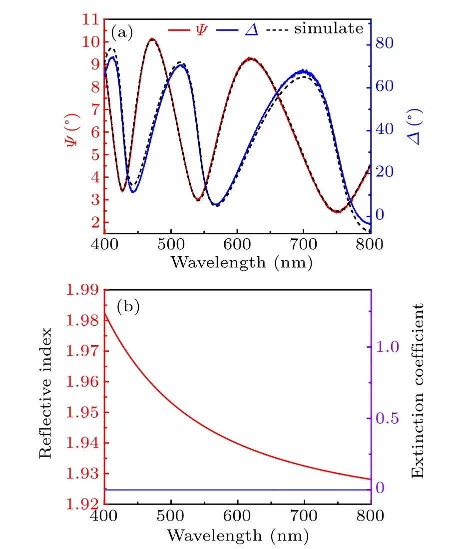
Figure 3 presents the spectroscopic ellipsometry data for the grown films. In SE measurement,as the light reflects from the sample, its polarization changes, which can be described by an amplitude ratio (Ψ) and a phase difference (∆). They are investigated by the equipment,and the film thickness and refractive index(n)could be deduced through a model fitting of the measured data.[41]As shown in Fig. 3(a),Ψ (red line)and ∆(blue line)are measured for a light wavelength ranging from 400 nm to 800 nm. Due to the excellent transparency of the Ga2O3films in the measured wavelength range, Cauchy relation is used as the ellipsometric analysis model to simulate the SE results[42]

where λ is the wavelength,and A,B,and C are the correlated coefficients. As seen in Fig. 3(a), a nonlinear curve simulation (black short dash curve) is performed perfectly when A,B, and C are equal to 1.916, 0.007, and 0.0005, respectively.Moreover,the variations of the refractive index(n)and extinction coefficient (k) with wavelength are obtained during the SE analysis. As shown in Fig.3(b),the extinction coefficients of the Si-doped Ga2O3films are set to zero and the refractive index n decreases slightly from 1.98 to 1.92, which are in agreement with the reported results.[41,43]With the SE measurement and analysis,the thickness of the deposited Si-doped Ga2O3films is estimated to be 532.4 nm. The thickness of the films suggests that the device could efficiently absorb the illumination in the UVC range.[44]

Fig.3. (a)SE signals Ψ (red line)and ∆(blue line)for β-Ga2O3 films at an incidence angle of 65.48°. The black short dash curve represents the simulated data produced by Cauchy model. (b)Refractive index n and extinction coefficient k of the β-Ga2O3 thin films.
As for the photoelectric properties, the carrier transport behavior of the device is measured by 4200 sourcemeter instrument under various illumination environments,and the results are plotted in Fig. 4. Figure 4(b) displays the current–voltage correlations under dark, 365 nm, and 254 nm radiation. It can be seen in the inset of Fig.4(b)that the dark current (Idark) of the device increases linearly with the voltage,suggesting good Ohmic contact between Ti/Au electrode and Si-doped Ga2O3films. The resistivity of the device is calculated to be 0.55 MΩ, which is smaller than the majority of undoped Ga2O3films(~TΩ). Hence it can be concluded that the dopant Si elements have efficiently enhanced the electric conductivity of the Ga2O3films. Moreover,the device shows slight photo-response under 365 nm illumination with a phototo-dark current ratio of ~6. When the films are exposed under 254 nm radiation, the photo-current approaches 16 mA under 20 V bias, which is two orders of magnitude larger than that measured in dark. Figure 4(c)illustrates the detailed photo-electrical characteristics of the device under different illumination intensities. As the light intensity increases from 200 µW/cm2to 2000 µW/cm2, the photo-current Iphotoincreases gradually from 11.2 mA to 21.7 mA at the bias of 20 V.In order to quantitatively gauge the optoelectrical properties of the photodetector,the responsivity of the device is calculated,and the results are drawn in Fig.4(d). The responsivity,which is a basic parameter to evaluate how well the photo-generated electron–hole pairs are generated, can be figured out by the following equation:[15]

where P is the light intensity and S is the effective irradiated section of the device. According to the schematic diagram of the device, the effective area is calculated to be 3.57×10⁻²cm2. As seen in Fig. 4(d), when the device is exposed under 254 nm UV illumination with a light intensity of 200µW/cm2,the responsivity ranges from 5.6 A/W to 788.9 A/W with the increase of the voltage. As the responsivity results are compared under the same applied voltage, it is found that the responsivity declines slightly with the increase of the light intensity. This phenomenon could be ascribed to the larger phonon–electron scattering and higher electron–hole recombination possibility induced by the self-heating behavior at the higher light intensity and the larger concentration of non-equilibrium carriers.[20,45]From these phenomena,it can be concluded that the Si-doped Ga2O3films exhibit excellent photo-response properties in the solar-blind region.
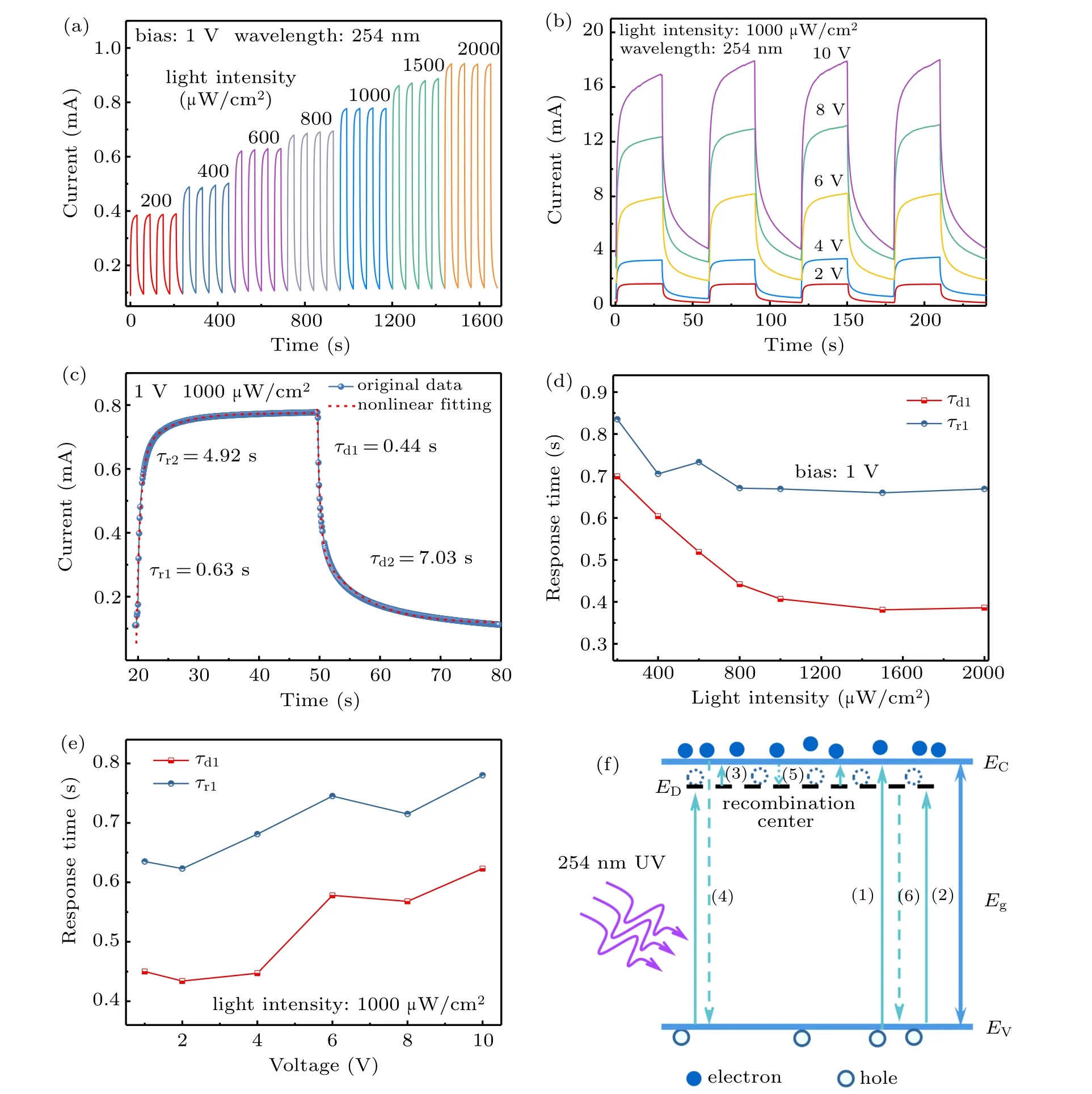
To assess the transient response time of the device, the time-dependent photo-response of the device is investigated with on/off switching of 254 nm light under various conditions,and the results are present in Fig.5.
Figure 5(a)illustrates the current of the device under varied light intensities at the forward voltage of 1 V. When the 200 µW/cm2254 nm radiation is turned on, the current goes up instantaneously to 0.39 mA. After the light is turned off,the current descends immediately. With the increase of the 254 nm light intensity, the photo-current of the detector rises monotonically from 0.39 mA to 0.94 mA.Moreover,when the films are exposed to 254 nm illumination with the light intensity of 1000 µW/cm2, the time-dependent photo-response diagram with various applied voltage is depicted in Fig.5(b).

Fig.4. (a)Schematic diagram of the MSM structured Si-doped Ga2O3 photodetectors. (b)Semi-logarithmic I–V characteristics of the device under dark,365 nm,and 254 nm illumination,the inset shows the corresponding I–V curve under the dark condition in linear scale. (c)Linear scale I–V behaviors of the device under 254 nm illumination with the intensity increased from 200 µW/cm2 to 2000 µW/cm2. (d) Detailed responsivity of the photodetector to 254 nm radiation under various light intensities.

Fig.5. The time-dependent photo-response of the detector(a)at 1 V bias under 254 nm illuminations with various light intensities,(b)under 1 mW/cm2 254 nm UV light illumination at various biases. (c) The original transient response data and nonlinear fitting about the rise and decay time of the device. (d) Response time of the device under various light intensities at a bias of 1 V. (e) Response time of the device under various voltages under 1000µW/cm2 254 nm illumination. (f)Schematic diagram illustrating the photoelectric mechanism in Si-doped Ga2O3 films.
With the increase of the applied voltage, the photo-current of the Si-doped Ga2O3films increases from 1.5 mA to 17.9 mA correspondingly. Stable photo-response characteristic in Figs.5(a)and 5(b)shows that the device exposed under various light intensities can be switched between on and off states with good reproducibility. Furthermore, the response time could be deduced by the fitting rise and decay edges of the time-dependent photo-response curve with a biexponential relaxation equation[10]

where I represents the stable photo-current, A and B are constants, τ1and τ2are two relaxation time constants. The rise time and decay time of the photodetector are denoted by τrand τd, respectively. To quantitatively extrapolate the response time in rise edge and decay edge, one cycle of the time-dependent photo-response of the device at 1 V bias and 1000 µW/cm2circumstance is extracted, and the fitting results are shown in Fig.5(c). It is clear that the rise time(τr1)and decay time (τd1) of the Si-doped Ga2O3films are 0.63 s and 0.44 s,respectively,indicating the decent response speed in UV detection. In addition, the response time of the device under various voltage and light intensity is figured out,and the results are plotted in Figs. 5(d) and 5(e). It can be found that the response time (τd1and τr1) decreases slowly with the increase of the light intensity,which may be attributed to the large carrier transport velocity.[46]Furthermore,the response time(τd1and τr1)increases gradually with the increase of the applied voltage, which could be ascribed to the persistent photoconductivity effect of the Si-doped Ga2O3films under high voltage.[47]To further elucidate the excellent photoresponse performance of the device, a schematic diagram is illustrated in Fig. 5(f). As Si elements are doped to Ga2O3films,Si prefers substituting to the tetrahedral coordination of the Ga1 site, leading to systematical increase of free electron density.[48]Moreover,Si dopants also behave as efficient shallow donor levels (less than 50 meV) in the energy band diagram. In Fig. 5(d), the upward solid arrows represent the generation of non-equilibrium carriers, while the downward dashed arrows denote the pathway for the carriers’ recombination. As the 254 nm UV illuminate on the Si-doped Ga2O3films,electron–hole pairs are generated and drifted to the electrode by the outside voltage. During this process,some photogenerated electrons jump from the valence band to the conduction band(process(1)),some electrons jump to the donor level (process (2)) and then transit to the conduction band(process (2)) because of the relatively low activation energy(≤50 meV). Hence more electron–hole pairs could be more easily generated. Meanwhile, doping Si elements may effectively reduce the contact resistance,and more photo-generated carriers could be transferred to the outside electrode before recombination again. Thus,the device exhibits a larger photocurrent and responsivity. Ga2O3film-based PDs are summarized in Table 1.[27,30,31,34,35,37,49]Compared with pure Ga2O3and Ga2O3doped with various impurities, Si-doped Ga2O3films in this work give decent response time and large photocurrent(up to mA order of magnitude), leading to large responsivity (up to 788 A/W). It is noted that the performance of the Si-doped Ga2O3based photodetector may also be enhanced by optimizing the fabrication parameters of the films or the structure of the photodetector.

Table 1. A brief summary of film-based Ga2O3 photodetectors.
4. Conclusion
The Si-doped Ga2O3films based MSM structured solarblind photodetector is demonstrated. The refractive index of the grown films is extracted to be 1.98–1.92 by spectroscopic ellipsometry measurement. The device gives large photocurrent ranging from 11.2 mA to 21.7 mA at 20 V bias and high photo-responsivity of 788 A·W−1under the illumination of 200 µW·cm−2intensity. Moreover, the rise and decay relaxation times are found to be 0.63 s and 0.44 s,indicating a decent response to UV illumination.All these results suggest the promising future in solar-blind photodetectors.
- Chinese Physics B的其它文章
- Process modeling gas atomization of close-coupled ring-hole nozzle for 316L stainless steel powder production*
- A 532 nm molecular iodine optical frequency standard based on modulation transfer spectroscopy*
- High-throughput identification of one-dimensional atomic wires and first principles calculations of their electronic states*
- Effect of tellurium(Te4+)irradiation on microstructure and associated irradiation-induced hardening*
- Effect of helium concentration on irradiation damage of Fe-ion irradiated SIMP steel at 300 °C and 450 °C*
- Optical spectroscopy study of damage evolution in 6H-SiC by H+2 implantation*

