Compact SPAD pixels with fast and accurate photon counting in the analog domain
Zhiqiang Ma,Zhong Wu,and Yue Xu,
1College of Electronic and Optical Engineering &College of Microelectronics,Nanjing University of Posts and Telecommunications,Nanjing 210023,China
2National and Local Joint Engineering Laboratory of RF integration &Micro-Assembly Technology,Nanjing 210023,China
Abstract:A compact pixel for single-photon detection in the analog domain is presented.The pixel integrates a single-photon avalanche diode (SPAD),a passive quenching &active recharging circuit (PQARC),and an analog counter for fast and accurate sensing and counting of photons.Fabricated in a standard 0.18 μm CMOS technology,the simulated and experimental results reveal that the dead time of the PQARC is about 8 ns and the maximum photon-counting rate can reach 125 Mcps (counting per second).The analog counter can achieve an 8-bit counting range with a voltage step of 6.9 mV.The differential nonlinearity(DNL) and integral nonlinearity (INL) of the analog counter are within the ± 0.6 and ± 1.2 LSB,respectively,indicating high linearity of photon counting.Due to its simple circuit structure and compact layout configuration,the total area occupation of the presented pixel is about 1500 μm2,leading to a high fill factor of 9.2%.The presented in-pixel front-end circuit is very suitable for the high-density array integration of SPAD sensors.
Key words:single-photon avalanche diode (SPAD);passive quenching &active recharging circuit (PQARC);analog counter;nonlinearity
1.Introduction
Measurement of weak optical signals utilizing singlephoton avalanche diode (SPAD) detectors have shown broad application prospects in different fields,such as quantum cryptography[1,2],Raman spectroscopy[3],light detection and ranging (LiDAR)[4,5],and 3-D imaging[6],etc.In some 2D array imagers like fluorescence lifetime imaging[7,8],a SPAD pixel usually consists of a quenching and recharging circuit,followed by an analog or a digital counter to sense and count photon avalanche events.To improve the detectable photon rate,a high-speed and high-reliability quench/recharge circuit is in great demand.Meanwhile,a compact photon counter is also greatly required to reduce the occupying area and enhance the pixel integration.
A simple quenching method is performed through a large integrated resistor,called a passive quenching circuit[9].However,the slow quenching speed,long recharging time,and high afterpulsing probability (AP) limit its applications.Although the literature reports many fast active quenching &recharging circuits (AQRCs)[10−13],all these solutions are based on the same approach that,to exploit a quick quenching for low AP probability,it needs a complex circuit structure with a large area occupation.
On the other hand,multi-pixel photon-counting applications require a high signal-to-noise ratio (SNR) and wide dynamic counting range.Although the digital photon counter attains significant advantages of high reliability,wide counting range,and high readout speed[14],it usually occupies a large area due to the use of a large number of transistors[15],resulting in a low fill factor.Fortunately,the analog counter as a promising alternative to the traditional digital counter has great potential to offer a high fill factor owing to simple circuit structure,however,it also faces the negative factors of mismatch,nonlinearity,noise,and parasitic effects[16−21].For example,a SPAD image sensor with analog counting pixel was reported for time-resolved fluorescence detection in 035-μm high-voltage CMOS technology,achieving a fill factor of 20.8%[18],nevertheless,the analog counter shows high pixel non-uniformity and the strong pulsewidth dependence of the output voltage step.Further,a compact analog counter was proposed based on the charge transfer method[19],reducing the influences of pulsewidth and period on the step size of the counter.However,the large MOS integral capacitance in the analog counter limits the pixel fill factor.Later,a 160 ×120 pixel analog-counting single-photon imager for fluorescence lifetime imaging was presented[20]using a 0.35μm standard CMOS process.A high fill factor of 21% is obtained,but the counting range is only 6-bit and the integral non-linearity deviation is also relatively large.After that,a 13-bit large dynamic range analog counter was implemented[21]with a count resolution of only 0.16 mV.
The purpose of this work is to achieve fast avalanche quenching and accurate photon-counting through a simple circuit structure.A high-speed PQARC for driving the SPAD device is presented,meanwhile,a compact analog counter with high linearity and large dynamic range is proposed,which are well verified through simulation analysis and experimental results.The main content of the paper is as follows.In Section 2,the circuit structure and principle of the pixel circuit are introduced.Section 3 analyzes the simulation and test results.Section 4 compares the circuit performance with the reported literature.Finally,conclusions are drawn in Section 5.

Fig.1.A front-end circuit diagram of SPAD pixel,including a PQARC and an analog counter.
2.Circuit description
The complete schematic of the SPAD pixel is shown in Fig.1,which includes a SPAD device and a front-end circuit consist of a PQARC and an analog counter.The PQARC for driving the SPAD device is composed of three transistors (MN1,MN2,and MN3),an inverter (INV1),and a delay line composed of multiple inverters in series.Fast passive quenching is achieved by a positive feedback loop formed by the transistors MN1,MN2,and the inverter INV1.The diode-connected MN1 provides an initial passive quenching resistance in the positive feedback loop.The function of the transistor MN3 and delay line is to recharge the SPAD device to the initial excess voltage state.The inverter INV2 shapes the avalanche pulse and outputs it to the analog counter.The analog counter consists of seven transistors (MP1,MP2,MP3,MN4,MN5,MN6,and MN7),two inverters (INV3 and INV4),and a capacitanceC.Among them,the reset circuit is composed of transistors MP1 and MP2,which plays the role of recharging node ‘b’ and the integral capacitanceC,respectively.Charge transfer is controlled by a pair of complementary transistors MP3 and MN4,inverter INV4,and transistor MN5.The inverter INV3 adjusts the input signal of the counter and isolates the PQARC from the counter.Transistor MN6 and MN7 act as the source follower and the column select switch,respectively,delivering the counting voltage on the integral capacitance to the column bus.
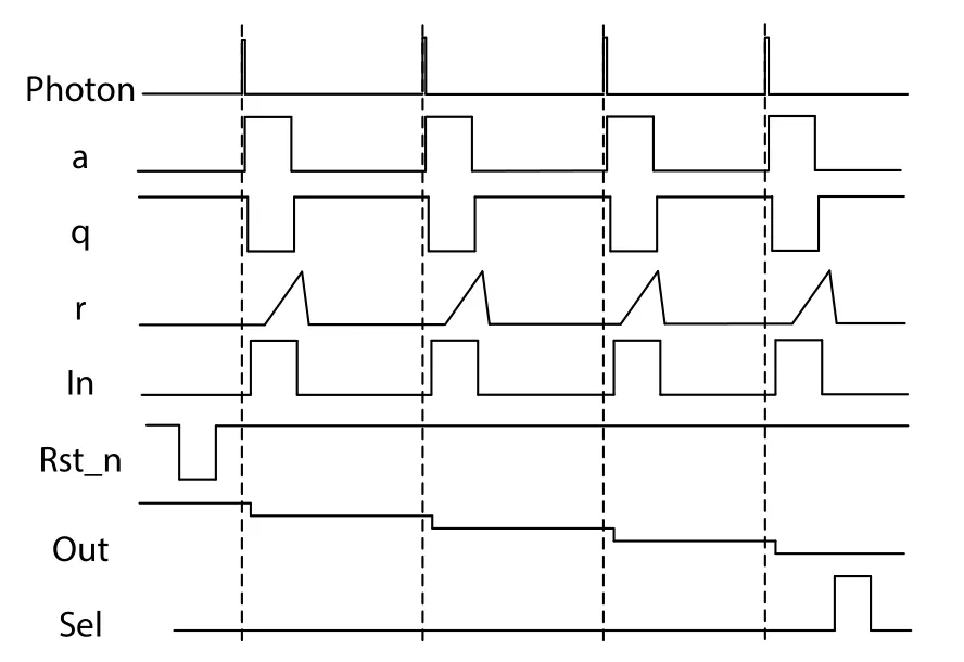
Fig.2.The timing diagram of pixel signals.
The operating principle of the pixel circuit is described as follows.Before the photon detection,the reset signal of the counter is valid (Rst_n=Low),the capacitanceCis charged to supply voltage.At this moment,the SPAD device is biased at an excess voltage state,and then the PQARC outputs a low level at node ‘i’.Once an incident photon is detected by the SPAD device,an avalanche event is triggered,and then the avalanche current quickly flows through the diode-connected transistor MN1 and transistor MN2.So,the anode voltage of the SPAD (at node ‘a’) begins to go up.Since the transistor MN2 provides a low-resistance path with its gate connected to high level,a current mirror between the NMOS in the inverter INV1 and the NMOS MN1 is established.The avalanche current is mirrored on the output of INV1,making the output voltage at node ‘q’ drop.With the reduction of the output voltage at node ‘q’,the channel resistance of transistor MN2 begins to increase,thus the SPAD anode voltage also increases.Due to the positive feedback loop,the rising speed of the SPAD anode voltage is accelerated.When the transistor MN2 is completely turned off,the avalanche current path is cut off and the SPAD device is rapidly quenched.After a short delay,the positive reset signal at node ‘r’ is generated,then the transistor MN3 is turned off and the anode voltage of SPAD is grounded,enabling the SPAD to return to the initial excess voltage state for next photon detection.This process will produce a sharp positive pulse at node ‘i’ for photon counting.The timing diagram of the pixel internal signals at different nodes is shown in Fig.2.
The analog counter determines the number of photons by recording the number of avalanche pulses.During the quenching period,SPAD anode node ‘a’ goes high,hence,a rising edge pulse is generated at node ‘i’ to drive transistors MP3 and MN4 to turn on and off,respectively,slightly delays the driving signal of the transistor MN4,avoiding the formation of a direct current path between the node ‘Out’and ‘Vc’,hence achieving charge transfer.As transistor MN4 turns on,a voltage change of (Vdd–Vc–VTH,MN4) will generate at node ‘c’.Accordingly,the amount of transferred charge ΔQis equal to
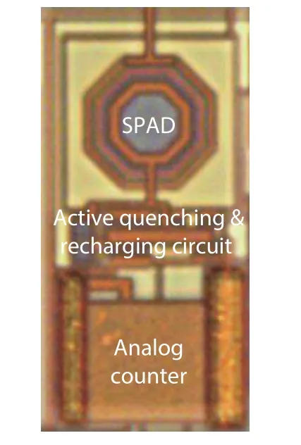
Fig.3.(Color online) Die micrograph of the compact SPAD pixel.

whereVTHMN4andCpare the threshold voltage of transistor MN4 and the parasitic capacitance from note ‘c’ to ground,respectively.After that,each avalanche event will draw a certain amount of charge ΔQfrom capacitanceC,and the voltage change ΔVouton capacitanceCis equal to

It can be found that the output voltage step of the analog counter is determined by the ratio of the parasitic capacitanceCpand the capacitanceC,and the value of the parasitic capacitanceCpis decided by the transistors MN4 and MN5.The circuit uses the smallest size transistors MN4 and MN5 to minimize the parasitic capacitanceCp.
During the reset of the PQARC circuit,node ‘i’ will go low,therefore the transistor MN5 is turned on,and the node‘c’ is recharged to the reference voltageVcagain.As a result,the counter goes back to its initial state and then repeats the counting operation as the photons arrive.The charge on the capacitanceCis thus gradually released,resulting in a descending step at the node ‘Out’.After the counting process is completed,the output voltage will be transmitted to the column bus through the source follower when select is valid (Sel=High).Finally,the number of photons is calculated based on the output voltage.
3.Experimental results
The presented SPAD pixel was designed and fabricated in SMIC 0.18-μm standard CMOS technology.Transistors MN1 and MN2 are designed to a minimum size (W=2Wmin,L=Lmin),which can effectively reduce the parasitic capacitance and enables high quenching speed.To accelerate the reset process of the SPAD,transistor MN3 selects a high aspect ratio (W=24Wmin,L=Lmin).Transistor MP3 acts as the switch for charge transfer,in which the minimum size (W=2Wmin,L=Lmin) is devised to reduce the effects of clock feedthrough and charge injection.Transistor MN4 selects a wide channel length (W=2Wmin,L=6Lmin) to lower leakage of charges on the capacitance,while transistors MN5 choose a minimum size (W=2Wmin,L=Lmin) to decrease parasitic capacitanceCp.Finally,the minimum MIM capacitanceCof 400 fF is adopted to ensure an 8-bit counting range while reducing the area occupation.
Fig.3 shows a micrograph of the proposed SPAD pixel,including an octagonal SPAD device with a 25-μm pitch,an AQRC,and an analog counter.To effectively save the area of the SPAD pixel,the MIM capacitance covers the layers of MOSFET transistors of the analog counter.Due to the simple circuit structure and compact layout,the areas of the AQRC and the analog counter are only 221 and 500μm2respectively,achieving the fill factor of the pixel up to 9.2%.
According to theI–Vcharacteristic curve,the avalanche voltage of the SPAD device is about 15.5 V and the test excess bias voltage is set to 3 V.Under this condition,the dark count rate (DCR) is about 6.9 kHz at room temperature,and the AP values are only 0.38%.The in-pixel PQARC was measured by illuminating SPAD with 532 nm incident-light,the photon detection efficiency (PDE) is approximately 23%.The transient avalanche pulses over a certain time window were observed by using a Tektronix MDO 3104 oscilloscope.Taking into account the load capacitance of the oscilloscope,the AQRC is followed by an internal output buffer to enhance the load driving capacity of the circuit.To precisely characterize the in-pixel analog counter,the input test signals of the analog counter are provided by XILINX's KINTEX-7 series FPGA and the output results of the analog counter are measured by a 12-bit off-chip analog-to-digital converter.
3.1.Characterization of quick quenching
The tested transient output waveform of the PQARC at an excess voltage of 3 V is shown in Fig.4(a).The output avalanche pulse of PQARC through the on-chip buffer is measured,showing a rising and falling edge time of 10.72 and 11.68 ns,respectively.Due to the load capacitance of the oscilloscope,the rising edge and falling delay time of the output avalanche pulse is greatly increased.To verify the correctness of the output avalanche waveform,the post-simulation of the PQARC was performed at the same excess voltage,considering an approximately 15 pF load capacitance from the chip PAD and oscilloscope probe.In this circuit simulation,a SPAD Verilog-A model was used to accurately emulate the avalanche behavior of SPAD devices[22].The simulated transient output waveform of Fig.4(b) is completely consistent with the tested waveform,indicating the correctness of the circuit function.Further,the simulated avalanche waveform without considering the on-chip buffer and the load capacitance is illustrated in Fig.4(c).Multiple consecutive avalanche pulses can be observed with 8 ns dead time,suggesting that the maximum photon-counting rate can reach 125 Mcps (counting per second).
3.2.Non-linearity estimation of the analog counter
To observe the linear photon counting mode,the readout voltage of the analog counter as a function of the photon pulse number was tested,as shown in Fig.5.Here,the input photon signal is generated by FPGA,with a pulsewidth of 40 ns for a period of 1μs.A very good linear relationship between the readout voltage and the photon number is observed.The readout voltage is linearly reduced from 3.24 to 1.49 V in the photon countering range from 0 to 256.An 8-bit counting resolution is achieved in the output voltage swing of 1.75 V,meaning the voltage step is about 6.9 mV per counting.It is also found that the measured data accords with the simulation results and there is only a slight difference between them.
The non-linearity was further characterized by using the tested data in Fig.5.The differential nonlinearity (DNL) and integral nonlinearity (INL) were calculated by the following formulas:
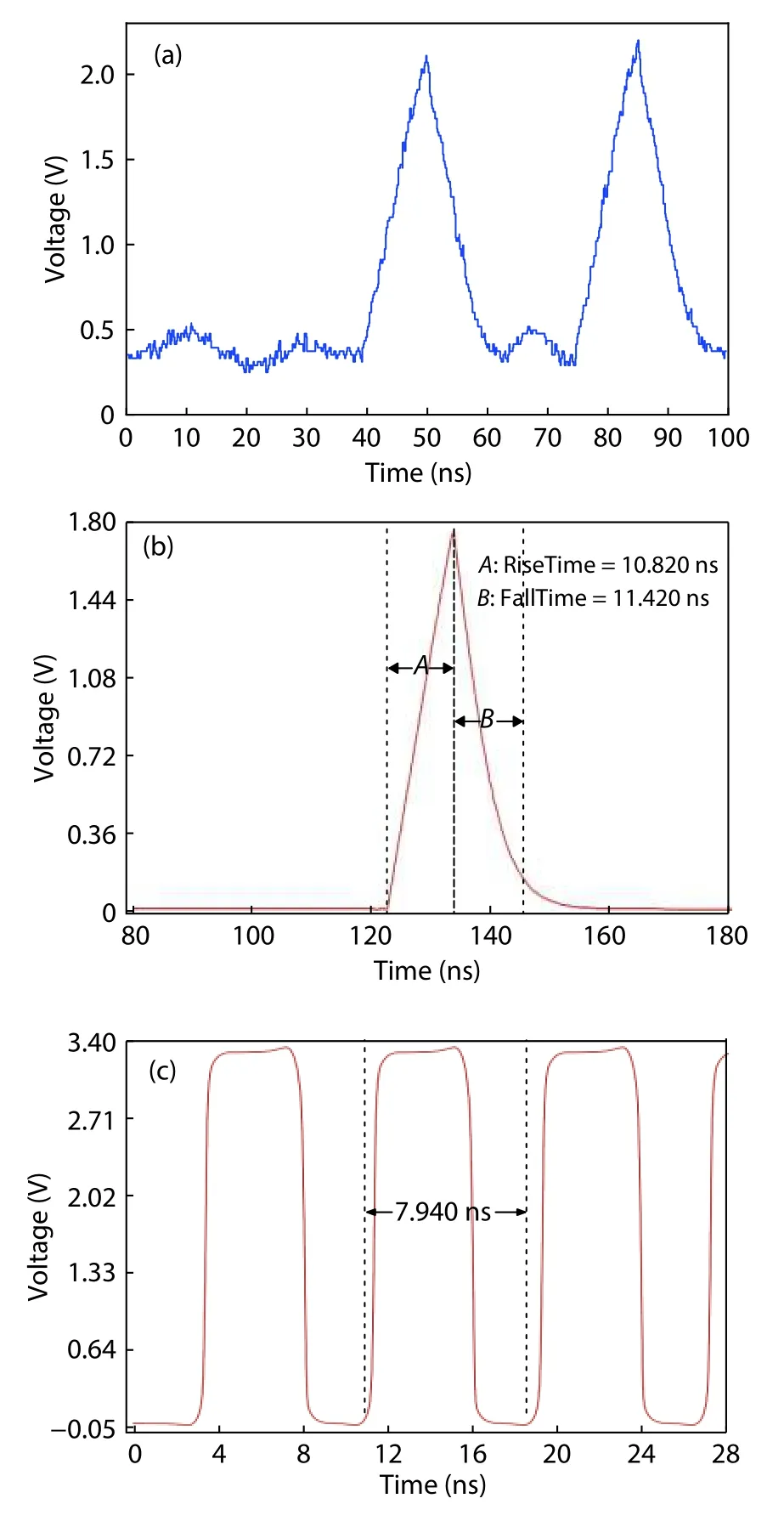
Fig.4.(Color online) Transient output avalanche pulse of the proposed quenching and recharging circuit.(a) Tested waveform.(b) Simulated waveform with on-chip buffer.(c) Simulated waveform without buffer.
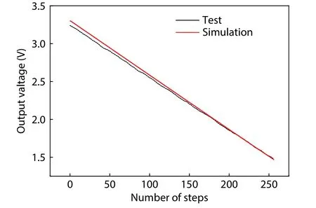
Fig.5.(Color online) Readout voltage of the analog counter as a function of the photon-counting number.


in which,ViandVLSBare thei-th output voltage value and average voltage step of the analog counter,respectively.
Fig.6 shows the DNL and INL of the analog counter.It can be seen that in the 8-bit counting setting,the DNL and INL are respectively less than ± 0.6 and ± 1.2 LSB,while the simulated DNL and INL are within ± 0.1 and ± 0.5 LSB,respectively.The larger tested nonlinearity is mainly due to the existence of power supply noise and ADC measurement errors in the actual measurement process.If excluding these factors,the circuit could achieve a lower nonlinearity,ensuring high precision counting of photons.
3.3.Pulsewidth and period dependence for the analog counter
It should be noted that the occurrence of avalanche events is random,therefore,the readout voltage step of the analog counter can be affected by the frequency of the avalanche pulses.To assess the influence,changing the input pulsewidth from 5 ns to 1μs and keeping the constant pulse period of 2μs,the pulsewidth dependence of the output voltage step was tested,as shown in Fig.7(a).In this wide range,the step size of testing and simulation increased by about 8.5% and 8.4% respectively,thus the test results are in good agreement with the simulation ones.Additionally,when the pulse width is maintained at 40 ns,the output voltage step as a function of the period of input pulses was measured with a varied period from 1 to 1000μs.The test results are shown in Fig.7(b).In the whole time range,the step changes of test and simulation are about 3.6% and 1.65% respectively and the test and simulation results are very close,which proves that the circuit performance reaches the desired results.
4.Discussions
Table 1 compares the key performance of the pixel presented in this work with the reported literature.The proposed pixel applies a simple circuit structure to achieve a high photon count rate,high linearity,low power consumption,and high fill factor.The passive quenching circuit senses the avalanche current through current sensing,which has a faster response speed than the voltage sensing method in Ref.[10].Also,during the quenching period,the quenching transistor MN2 is turned off through a positive feedback loop,directly breaking the avalanche current path to accelerate quenching for a minimum dead time of 8 ns.Compared with Ref.[13],the circuit structure of the PQARC is simpler and suitable for high-density array integration.The analog counter based on the charge transfer method achieves a count range of 8 bits,which is higher than that in Refs.[16,20].The analog counter uses a pair of complementary transistors MP3 and MN4 as charge transfer switches and uses a delay inverter INV4 to control the conduction of the transistors,effectively preventing short-term charge leakage during circuit conversion,and realizing charge transfer to improve output linearity.Compared with the implementation in Ref.[18],the counting method based on charge transfer solves the problem of the input analog count step being affected by the input avalanche pulsewidth,and the dependence on the input avalanche pulsewidth within the count range of 8 bits is reduced from 9.4% in Ref.[19]to 8.5%.At the same time,the voltage swing of 1.75 V guarantees a high voltage resolution,which has higher noise immunity compared to the photon resolution of 0.16 mV in Ref.[21].Due to the simple circuit structure,the entire pixel circuit occupies a layout area of 1500μm2and achieves low power consumption,obtaining a high fill factor of 9.2% and low power consumption of 38.2μW,which is superior to the results reported in the literature[20,21].
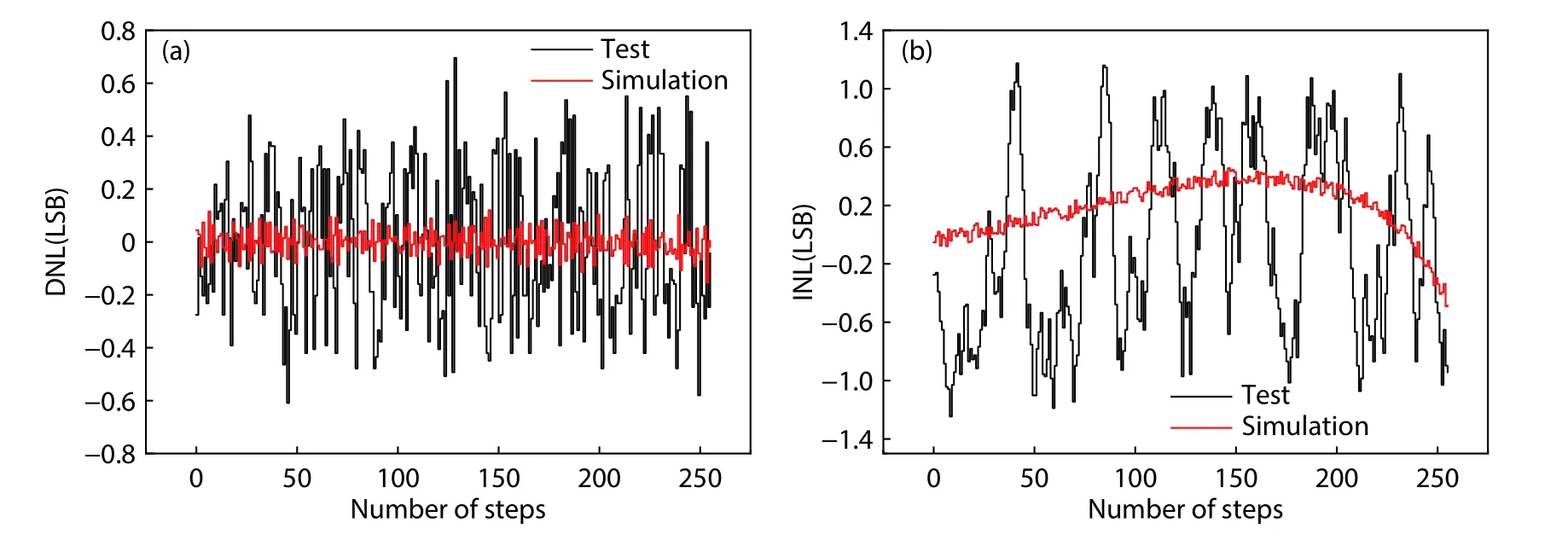
Fig.6.(Color online) Non-linearity characteristics of the analog counter.(a) Differential non-linearity (DNL).(b) Integral non-linearity (INL).
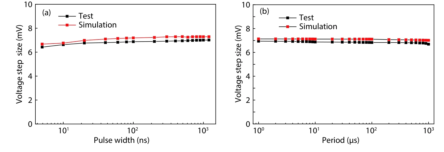
Fig.7.(Color online) Output voltage step size as a function of (a) pulsewidth and (b) period for the analog counter.

Table 1. Summary of performance Comparison with SPAD pixels reported in the literature.
5.Conclusion
A compact pixel including a SPAD,a PQARC,and an analog counter is proposed for single-photon detection in the analog domain.Fabricated in SMIC 0.18μm standard CMOS process,the test results show that the PQARC can reach a maximum photon counting-rate of 125 Mcps and the analog counter can achieve an 8-bit counting range with a voltage resolution of 6.9 mV.The DNL and INL are lower than ± 0.6 and ± 1.2 LSB,respectively,and the pulse width and period dependence of voltage steps are less than 8.5% and 3.6%,respectively,which ensures the high-precision counting.Due to the simple circuit structure and compact configuration,the area occupation of the SPAD pixel is about 1500μm2,the fill factor is up to 9.2%,and the power consumption is as low as 38.2μW.Owing to the high photon counting-rate,high counting linearity,small area,and low power consumption,the proposed pixel is particularly suitable for a high-density SPAD array integration based on standard CMOS technology.
Acknowledgements
This work was supported by the National Natural Science Foundation of China (No.61571235,61871231) and the Key Research &Development Plan of Jiangsu Province,China(No.BE2019741),and the Natural Science Foundation of Jiangsu Province,China (No.BK20181390).
 Journal of Semiconductors2021年5期
- Journal of Semiconductors的其它文章
- WO3 passivation layer-coated nanostructured TiO2:An efficient defect engineered photoelectrode for dye sensitized solar cell
- A complete small-signal HBT model including AC current crowding effect
- Facile fabrication of heterostructure with p-BiOCl nanoflakes and n-ZnO thin film for UV photodetectors
- Morphology and crystalline property of an AlN single crystal grown on AlN seed
- A crossover from Efros–Shklovskii hopping to activated transport in a GaAs two-dimensional hole system at low temperatures
- Recent progress of physical failure analysis of GaN HEMTs
