WO3 passivation layer-coated nanostructured TiO2:An efficient defect engineered photoelectrode for dye sensitized solar cell
Arya Babu,Arya Vasanth,Shantikumar Nair,and Mariyappan Shanmugam
Amrita Centre for Nanosciences and Molecular Medicine,Amrita Vishwa Vidyapeetham,Kochi,Kerala -682041,India
Abstract:Major loss factors for photo-generated electrons due to the presence of surface defects in titanium dioxide (TiO2)were controlled by RF-sputtered tungsten trioxide (WO3) passivation.X-ray photoelectron spectroscopy assured the coating of WO3on the TiO2nanoparticle layer by showing Ti 2p,W 4f and O 1s characteristic peaks and were further confirmed by X-ray diffraction studies.The coating of WO3on the TiO2nanoparticle layer did not affect dye adsorption significantly.Dye sensitized solar cells (DSSCs) fabricated using WO3-coated TiO2showed an enhancement of~10% compared to DSSCs fabricated using pristine TiO2-based photo-electrodes.It is attributed to the WO3passivation on TiO2that creates an energy barrier which favored photo-electron injection by tunneling but blocked reverse electron recombination pathways towards holes available in highest occupied molecular orbital of the dye molecules.It was further evidenced that there is an optimum thickness (duration of coating) of WO3to improve the DSSC performance and longer duration of WO3suppressed photo-electron injection from dye to TiO2as inferred from the detrimental effect in short circuit current density values.RF-sputtering yields pinhole-free,highly uniform and conformal coating of WO3onto any area of interest,which can be considered for an effective surface passivation for nanostructured photovoltaic devices.
Key words:charge transport;recombination;tungsten oxide;solar cell;interface;defects
1.Introduction
The most important technological arrival of nanotechnology has endorsed multifarious nanostructured functional materials for energy conversion applications[1−4].Nanostructured functional materials have been showing superior characteristics in terms of structural,optical,electrical and mechanical perspectives[5−8].Size-dependent properties of nanomaterials and their consequences on various applications have been realized as a potential possible approach to improve performance of resulting products including photovoltaics,sensors,batteries and light-emitting diodes[2,9−11].However,it has been observed that nanostructures,such as particles,fibers and planar materials,exhibit surface sensitive characteristics due to the presence of chemically unsaturated defect states which are established through the modified surface-tovolume ratio[12−16].Such remarkable changes over the surface of functional materials lead to unavoidable degeneracies,including surface states which can have energy distribution throughout the bandgap of resulting materials[17−21].Surface states in a material plays a critical role on charge transport and recombination as they are electronically active mostly in the vicinity of band-edges[22,23].However,nanostructured functional materials cannot be avoided in energy conversion devices as they show dominant optical and electrical transport characteristics which are highly preferred specifically for light-matter interaction[24−26].Thus,alternate measures are required to employ such attractive materials for energy-related applications and those measures are expected to control the detrimental effects of surface defects on charge transport to minimize the recombination loss.A surface with active unsaturated dangling bonds is highly sensitive to charge transport in solar cells and thus it is an essential factor to passivate/modify using appropriate methods[27−30].
A variety of metal oxides and dielectrics were used in DSSCs to control the recombination at TiO2/dye/electrolyte interfaces[30−38].Thickness,dielectric properties,surface coverage and electronic quality of the passivation layers have been studied and reported to be considered as dominant factors which determine the ability to control the defects[39−44].Wetchemical methods such as hydrothermal process,physical vapor deposition techniques,including RF/DC sputtering,electron beam/thermal evaporation and chemical vapor deposition,were widely used to apply passivation on functional materials such as TiO2in DSSCs[45−49].Atomic layer deposition has been identified as a superior technique to passivate nanostructured defective material as it often yields ultra-thin (few atomic layers) high-quality dielectrics which can be conformally coated onto any randomly distributed nanostructures[50,51].The highly conformal surface coverage results in efficient passivation which controls the detrimental role of defects on charge transport in DSSCs[52−54].
The present work identified tungsten oxide (WO3) as a possible wide bandgap material which can be used for effective surface passivation on TiO2to modify the surface to achieve better control over defects.Resultsshowed the possibility of improving DSSC performance by coating WO3via RF-sputtering on TiO2in which defects are most dominating in terms of interfacial recombination.

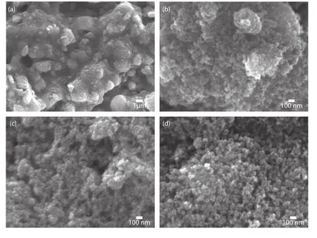
Fig.1.Surface morphology of pristine TiO2at the magnifications of (a) 1000× and (b) 40 000× showing macroscopic clusters and agglomerated particles respectively,(c,d) WO3coated TiO2nanoparticles layer showing randomly distributed TiO2nanoparticles and the porous nature.
2.Experimental section
Commercially available fluorine-doped tin oxide (FTO)glass substrates were used for DSSC fabrication process.The FTO-coated glass substrates were cleaned by sonicating them in soap solution for 15 min,then in DI water and finally with ethanol for 15 min to remove all sort of contaminations.The cleaned FTO-coated glass substrates were kept in an oven for drying at 72 ˚C.Colloidal TiO2paste was prepared by mixing the required amount of TiO2powder (Sigma Aldrich,99.9% purity) and polyethylene glycolate (PEG).Both were mixed and ground thoroughly using a mortar and pestle until a required form of colloidal paste was obtained.TiO2colloidal paste was doctor-bladed onto FTO-coated glass substrates using adhesive tape as a shadow-mask,which were removed after making the TiO2films.Colloidal TiO2films coating the FTO samples were then annealed at 450 ˚C for 3 h with a ramp rate of 3 ˚C per minute.
WO3thin film was coated on TiO2nanoparticle films using the RF sputtering technique.Samples were fixed on the substrate holder using temperature-sustainable,vacuum-compatible Kapton tape.They were placed in the RF-sputter chamber in which tungsten was used as target with oxygen as a bombarding process gas.The oxygen gas flow rate was maintained at 70 sccm with a FR-power of 25 W.To assess the effect of thickness of WO3surface passivation on TiO2,the present study varied the thickness values of WO3to 15,22,and 30 nm on TiO2.This thickness variation was achieved by varying the duration of WO3coating on TiO2for 7,10,and 15 min.The WO3-coated TiO2nanoparticle layer on FTO was removed from the RF-sputter chamber and annealed at 120 ˚C.
In the present work,two categories of DSSCs were fabricated using (i) pristine TiO2and (ii) WO3-coated TiO2to validate the effect of WO3passivation on TiO2nanoparticle layer in DSSC performance.Ruthenium-based N719 dye was prepared using a mixture of 50 mL of tert-butyl alcohol and 50 mL of acetonitrile.Then,0.5 mM of N719 dye (59.43 mg for 100 mL) was added and stirred for 30 min to make the required homogeneous N719 dye.The pristine TiO2and WO3-coated TiO2samples prepared on FTO-coated glass substrates were immersed in dye solution to sensitize.DSSCs were fabricated using N719-adsorbed pristine TiO2and WO3-coated TiO2as photo-anodes to compare the effect of WO3passivation.Hole-transporting iodide/tri-iodide was used as an electrolyte along with a platinum counter electrode for the DSSCs.The only difference between the two categories of DSSCs was the WO3passivation on the TiO2nanoparticle layer.
Surface morphology of the pristine and WO3-coated TiO2samples were characterized using a JSN 7610S Plus JEOLJSM-6490-LA scanning electron microscope (FESEM).X-ray photoelectron spectroscopy (XPS) used a Kratos Analytical unit.X-ray diffraction (XRD) patterns of the WO3coated samples were obtained using PANalytical X’Pert PRO X-Ray Diffractometer.UV–visible optical spectra of the samples were obtained in a Perkin Elmer Lambda-750 UV–visible spectrometer.The fabricated DSSCs were characterized under 1-Sun illumination (AM 1.5 G) in a Newport Oriel Class A solar simulator to measure requiredJ–Vcharacteristics using a Keithley-2420 digital source meter.
3.Results and discussion

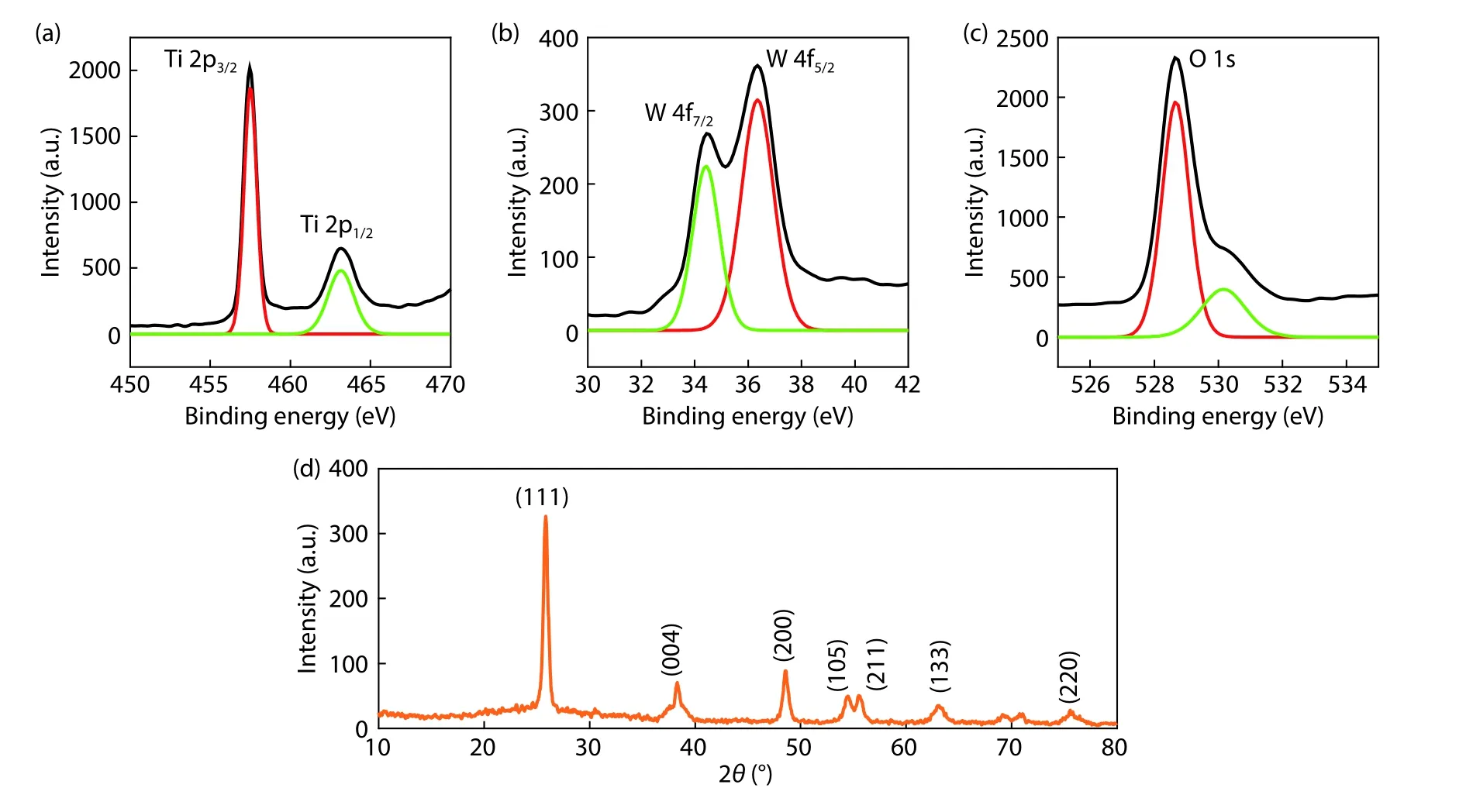
Fig.2.(Color online) (a–c) High resolution XPS scans showing Ti 2p,W 4f and O 1s peaks from the WO3coated TiO2sample.(d) XRD pattern obtained from the same sample.
Figs.1(a) and 1(b) show surface morphology of the TiO2nanoparticle layer coated on the FTO substrate for DSSC fabrication.Macroscopic clustered TiO2was observed at the low(1000×) magnification in Fig.1(a),and a further magnified image exhibited smaller size TiO2particles agglomerated on the macroscopic clusters as shown in Fig.1(b) which was obtained at the magnification of 40 000×.While the lower magnified image exhibited a macroscopic cluster film,the higher one showed the nanoparticles agglomerated as clusters.Figs.1(c) and 1(d) were obtained from the TiO2nanoparticle layer after coating the WO3passivation layer at 15 and 30 nm,respectively.It is evident that the coating of thin WO3on the TiO2nanoparticle layer did not change the morphology significantly in terms of surface morphology.The WO3coating was performed by RF-sputtering,which is a gas-phase plasma assisted physical vapor deposition process to achieve uniform coating of functional material.The surface morphology images shown in Figs.1(c) and 1(d) clearly addressed the pristine nature of the TiO2nanoparticle layer was not modified as the RF-sputtering process uniformly covered the TiO2nanoparticles and the coating did not block the porosity of the TiO2,as can be seen in Figs.1(a) and 1(b).In general,the surface passivation coating is applied on nanostructured functional materials in which defects are playing a dominated role on charge transport characteristics and deteriorates the performance of the resulting solar cells.Thus,it is essential to coat the surface passivation layer but if it is too thick or not uniform then the surface passivation layer itself might block the charge transport and thus recombination would dominate.In the present study,the surface morphology images prove that WO3did not affect TiO2morphology as it was thin enough and uniform.
Fig.2 shows results from XPS and XRD studies performed on the WO3-coated TiO2nanoparticle layer.Fig.2(a)shows a high-resolution XPS scan obtained from the sample showing Ti 2p peaks.Specifically,Ti 2p3/2and Ti 2p1/2were 457.4 and 463.1 eV respectively,showing the spin-orbital splitting of photoelectrons. The binding energy difference between two peaks was 5.7 eV.Fig.2(b) shows a high-resolution XPS scan of tungsten (W) which belongs to the WO3passivation layer on the TiO2nanoparticle layer.The spin-orbital splitting of photoelectrons exhibited W 4f7/2and W 4f5/2at the binding energy values of 34.4 and 36.3 eV respectively.The energy difference between the two peaks was observed to be 1.9 eV.The high-resolution XPS scan showing O 1s spectrum obtained from the sample is shown in Fig.2(c).The peak occurred at 528.7 eV.All these characteristic peaks,identified with respect to their binding energy values,confirmed the WO3coating on the TiO2nanoparticle layer.Fig.2(d)shows XRD pattern of the WO3-coated TiO2nanoparticle layer.The XRD peak appeared at 2θof 25.8° represents (101)which corresponds to the anatase TiO2phase and this was confirmed from JCPDS-84-1286.The TiO2is considered to be phase pure as it did not show the rutile phase at 2θvalue of 27.36°.Further the XRD peaks at 2θvalues of 38.3° (004),48.5° (200) and 55.6° (211) also assert the TiO2nanoparticle layer.The indices (105),(133) and (220) at 2θvalues of 54.4°,63.1°,75.5° represent the WO3thin film coating on the TiO2nanoparticle layer.Thus,the XRD pattern obtained from the WO3passivation thin film-coated TiO2nanoparticle layer also confirmed both the functional materials with respective to their characteristic peaks.

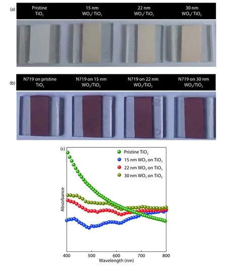
Fig.3.(Color online) Digital photographic images of (a) TiO2nanoparticle layer coated on FTO covered glass substrates showing the deposition of WO3surface passivation layer with different thickness values.(b) Photographs of the samples after N719 dye coating confirming the WO3did not affect the loading much.(c) UV–visible absorption spectra of the samples.
Fig.3(a) shows photographs of the pristine TiO2nanoparticle layer along with 15,22,30 nm WO3-coated TiO2.It was very obvious that WO3passivation was thin enough,which did not change the TiO2much in terms of the color.However,it was very clear from the picture that WO3was coated on the surface of the TiO2nanoparticle film.In this study,WO3was coated on TiO2to modify/suppress the defects which are actively participating in the charge transport process in DSSCs.Thus,it was a genuine expectation that WO3should not affect the dye adsorption on the surface of TiO2.The photograph shown in Fig.3(b) shows the pristine TiO2nanoparticle layer along with 15,22,and 30 nm WO3-coated TiO2after the dye loading process.It provided evidence that coating of WO3on the TiO2nanoparticle layer did not affect the dye loading significantly.In general,a surface passivation layer is expected to control the defects in semiconductors to improve the charge transport characteristics to yield high performance photovoltaic devices.If the dye loading into the TiO2nanoparticle layer is impeded by WO3,then exciton generation will be reduced significantly which,in turn,would result in lower photo-current and overall performance.Fig.3(c) shows UV–visible optical absorption spectroscopic measurements performed on the pristine TiO2nanoparticle layer in comparison with TiO2samples coated with the 15,22,and 30 nm WO3surface passivation layer.As shown in the Fig.3(c),the pristine and WO3-coated TiO2did not show any significant absorption in the spectral window of 400–800 nm in which a major portion of visible energy photons are available.Thus,passivating TiO2by WO3will not impede visible spectral photons to reach dye molecules to generate excitons.Thus,WO3coating on TiO2can be categorized as an advantage for DSSC operation in terms of defect passivation but has no disadvantage in terms of absorption loss due to the optimum band structure characteristics.In DSSCs,incident photons enter through a transparent electrode,FTO,and travel through the TiO2nanoparticle layer to reach organic dye to generate excitons.Passivation layers are coated on TiO2in DSSCs to control defects.If the passivation layer scatters or disperses photons between TiO2and dye,it will lead to major optical loss which would affect the photocurrent generation.Thus,it is important to confirm the passivation layer does not interact with incident photons in the visible spectral range.Further,UV–visible spectra of WO3-coated TiO2samples exhibited that absorption at the high energy spectral region was significantly suppressed after WO3coating.WO3exhibits an optical bandgap in the range of 2.6–3 eV.When pristine TiO2showed absorption in the high energy range,WO3coating suppressed the exciton generation at this specific range due to the heterostructure alignment in the band-structure[55].It could be attributed to the thermalization effect which also contributed to the increment in the absorption of photons in the longer wavelength regions.This effect was observed in all three TiO2samples with WO3coating.

Fig.4.(Color online) (a) J–V characteristics of the DSSC with and without WO3passivation on TiO2.(b) Comparison of PMAXof DSSCs,dark current characteristics of DSSCs in (c) linear and (d)semi-log scale showing the saturation current values.

Table 1. Photovoltaic parameters of the DSSCs measured under AM1.5 illumination level.
Fig.4(a) shows illuminatedJ–Vcharacteristics of the DSSCs which used pristine TiO2as a photo-anode along with the WO3passivation layer-coated TiO2.The illuminatedJ–Vcharacteristics of the DSSCs showed that coating of WO3on the TiO2nanoparticle played a significant role in terms of all photovoltaic parameters including open circuit voltage (VOC),short circuit current density (JSC),fill factor (FF) and efficiency(η).All the key photovoltaic parameters measured under AM 1.5 illumination are listed in Table 1 along with standard deviation inη.The reference DSSC,which used a pristine TiO2-based photo-anode (no WO3coating),resulted inVOC,JSC,FFandηof 745 mV,9.3 mA/cm2,59.0%,and 4.1% respectively.The DSSC,which used 22 nm coating of WO3on TiO2as a photo-anode,resulted inVOC,JSC,FFandηof 712 mV,11.1 mA/cm2,57.2%,and 4.5%,respectively.This is approximately 10% enhancement in η due to the increment inJSC.As can be seen in Table 1,further increment in the duration of WO3coating on TiO2affected photovoltaic parameters significantly.It can be directly attributed to the reduction inJSCby creating a thicker energy barrier between the TiO2and dye where the charge carrier injection occurred.It is well known that if the energy barrier thickness increases,then tunneling probability would decrease.Thus,an optimum thickness of the passivation layer is required to passivate the defects.In the present study,it was found that 10 min WO3coating on TiO2performed better than other DSSCs.

Fig.5.(Color online) Schematic illustration of (a) FTO/TiO2/dye/electrolyte and (b) FTO/TiO2/WO3/Dye/electrolyte interfaces in DSSCs showing electron–hole transport and recombination mediated by defects in TiO2.
Fig.4(b) shows power density–voltage characteristics of the reference DSSCs along with DSSCs used WO3passivation showing the maximum power point (PMAX) values.It was noticed that DSSC used 10 min of WO3passivation on TiO2resulted in 4.5 mW/cm2while the reference DSSC exhibited 4 mW/cm2.This is one of the parameters along with the increment inJSCimproved the~10% enhancement inηfor the DSSC with 22 nm WO3passivation on TiO2.The DSSC with 15 min of WO3passivation showed 3.8 mW/cm2.It clearly indicated that increasing thickness of WO3affected thePMAXand thus the detrimental effect on photovoltaic performance.Fig.4(c) shows dark current–voltage characteristics of the DSSCs with a semi-log plot of the same in the higher applied range of 0.7 to 1 V.It is possible to assess the electronic quality of interfaces in DSSCs through dark saturation current (IO)which can be obtained from the generalID=IOexp(qV/kT–1),whereIDandIOare current density and saturation current respectively under dark conditions.The parameters in equationq,V,kandTare electronic charge,applied bias to the DSSCs,Boltzmann constant and temperature at which the DSSCs work respectively.It is well known that DSSCs with good quality interfaces exhibit higherIOvalues at higher applied bias regions,lowerIOvalues at lower and medium forward bias regions.IncreasingIOin the low and medium forward bias regions can directly be attributed to the defect dominated charge transport.Thus,the parameter (IO) needs to be suppressed to obtain a DSSC with improved photovoltaic performance.Inset in Fig.4(c) clearly showed the DSSC with 10 min WO3coating resulted in higherIOvalue compared with other DSSCs.Fig.4(d) shows semi-log plots of dark current characteristics of the reference DSSC along with DSSC used WO3passivation.We have chosen the applied bias region close to 0.3 V to consider theIOvalues for the DSSCs.It is evident that DSSC with 10 min of WO3passivation on TiO2exhibited 1 × 10⁻⁷A,which is 20 times lower than theIOvalues showed by reference DSSC which was 2 × 10⁻⁶A.In this calculation,0.3 V applied bias has been considered to extract theIOvalues for all DSSCs for the reason that a linear dark current increment was observed in the semi-log plot as shown in Fig.4(d).If the dark current is highly linear in the log-scale,it is a perfect exponential diode characteristic feature.Thus,the applied bias of 0.3 V has been used to extractIOvalues.
Figs.5(a) and 5(b) show the energy level diagram representing FTO/TiO2/dye/electrolyte and FTO/TiO2/WO3/Dye/electrolyte interfaces respectively.The only difference between the two categories of DSSCs examined in the present work was WO3passivation on TiO2.Thus,the variation in photovoltaic performance is directly attributed to the ability of WO3to passivate defects in TiO2.Photo-generated electrons in the lowest unoccupied molecular orbital (LUMO) of the dye need to be injected into the conduction band edge of TiO2(EC) in which they are all transported to reach the FTO electrode by diffusion as represented by process (1).Meanwhile,the holes from the highest occupied molecular orbital (HOMO) of the dye will be regenerated by the electrolyte as shown in process (2).These two categories are electron and hole transport,which eventually contribute to photo-current in DSSCs.However,the photo-electrons in the bulk of TiO2nanoparticle layer can be trapped by defects present in the bandgap of TiO2as illustrated by process (3).If the trap states,which are close to the trapped electron,can trap a hole from the HOMO of the dye as shown in process (4),then electron-hole recombination will occur at the bandgap of TiO2mediated by defects.Fig.5(b) shows the possible changes that can occur at the electron–hole transport and recombination kinetics after coating the WO3surface passivation layer on TiO2.The photo-generated electron injection from the LUMO of the dye will be injected through the WO3surface passivation layer by tunneling as the thickness is facilitating such a transport process.Photo-generated electrons in the TiO2further can be trapped by defects but the probability of hole trapping,process (4),is rather difficult as the WO3will not allow the trap states in TiO2to interact with holes at the HOMO of the dye.Thus,hole trapping will not occur at the TiO2/dye interface after coating the passivation layer.The photo-generated electron will not be lost without having a hole in the bulk vicinity of TiO2.The probability of recombination loss is expected to be suppressed by coating a thin WO3film on TiO2.This situation will lead to improved DSSC performance.
4.Conclusion
A dominant recombination pathway at the TiO2/dye interface was significantly suppressed by passivating the TiO2surface using RF-sputtered WO3film.RF-sputtering is a versatile technique to coat WO3surface passivation on the TiO2nanoparticle layer without blocking the porosity.DSSC with WO3passivation exhibited~10% enhancement in performance.Results from DSSCs confirmed that there is an optimum thickness of WO3,at which the electron-hole transport was facilitated while the recombination probability was reduced.
Acknowledgements
We thank the Amrita Centre for Nanosciences for providing us with the PVD cluster equipment to coat various functional thin films for the energy conversion technology development.
 Journal of Semiconductors2021年5期
- Journal of Semiconductors的其它文章
- Compact SPAD pixels with fast and accurate photon counting in the analog domain
- A complete small-signal HBT model including AC current crowding effect
- Facile fabrication of heterostructure with p-BiOCl nanoflakes and n-ZnO thin film for UV photodetectors
- Morphology and crystalline property of an AlN single crystal grown on AlN seed
- A crossover from Efros–Shklovskii hopping to activated transport in a GaAs two-dimensional hole system at low temperatures
- Recent progress of physical failure analysis of GaN HEMTs
