
A complete small-signal HBT model including AC current crowding effect
2021-05-19 06:40:28JinjingHuangandJunLiu
Journal of Semiconductors 2021年5期
Jinjing Huang and Jun Liu
Key Laboratory of RF Circuits and Systems,Ministry of Education,Hangzhou Dianzi University,Hangzhou 310018,China
Abstract:An improved small-signal equivalent circuit of HBT concerning the AC current crowding effect is proposed in this paper.AC current crowding effect is modeled as a parallel RC circuit composed of Cbiand Rbi,with distributed base-collector junction capacitance also taken into account.The intrinsic portion is taken as a whole and extracted directly from the measured Sparameters in the whole frequency range of operation without any special test structures.An HBT device with a 2 × 20 μm2 emitter-area under three different biases were used to demonstrate the extraction and verify the accuracy of the equivalent circuit.
Key words:small-signal model;HBT;AC current crowding effect
1.Introduction
Heterojunction bipolar transistors (HBTs) have been extensively used in high-speed analog,digital and mixed-signal integrated circuits (ICs)[1−4].There are several small-signal equivalent circuit topologies for microwave HBT devices’ modeling and the accuracy of small-signal model plays a crucial role in the design of ICs.
However,most of the reported topologies ignore the AC current crowding effect[5],which is a critical factor for predicting the AC performance of HBT devices,especially in high frequency range.AC current crowding occurs in the high frequency range related to the bypassing effects of base-emitter capacitance.As the small-signal voltage drops along the intrinsic base region,the diffusion capacitance at the edge of the emitter is proportionally higher than that at the center.This phenomenon can cause the small-signal emitter current to crowd near the edge of the base-emitter junction as frequency increases.Therefore,the intrinsic base capacitance is physically connected with the AC current crowding[6].
In recent years,different small-signal equivalent circuits have been proposed with various extraction methods,in which π[7]or T[8,9]topologies were used to represent the small-signal equivalent circuits.Heunget al.[10]proposed a simple extraction method by using the RC circuit to characterize the AC current crowding effect.However,a simple π-type topology was adopted to extract the intrinsic base capacitance (Cbi) through theZ-parameter equations.In addition,other papers[11−14]have proposed a more complete small-signal model compared with Ref.[10].Although their methods have shown good accuracy in the extraction process,more cumbersome analytical methods and calculation cost were needed.Zhanget al.[15]proposed a rigorous but concise peeling extraction algorithm.While this method failed to consider the AC current crowding effect,this paper proposes an accurate extraction method with a complete π-type small-signal equivalent circuit considering the AC current crowding effect.This new equivalent-circuit topology is developed based on the small-signal equivalent circuit of an AHBT (agilent heterojunction bipolar transistor) model which has considered the distributed base-collector junction capacitance.Based on the peeling algorithm in Ref.[15]and the T-π transformation presented in Refs.[16–18],a novel method is proposed.In Section 2,an integral small-signal model taking into account the AC current crowding effect is introduced.The parameter extraction procedure is presented in detail in Section 3.Section 4 validates the model performance and a comparison between the proposed model and the conventional model withoutCbi.Finally,a conclusion is given in Section 5.
2.Small-signal model
The complete small-signal equivalent circuit of the HBT device considering the AC current crowding effect is given in Fig.1.
In Fig.1,Rbx,Rcx,Reare the base,collector,and emitter parasitic resistances,respectively.RbcxandRbexare the extrinsic base-collector and base-emitter resistances,andCbcxandCbexare the extrinsic base-collector and base-emitter depletion capacitances.RbiandRciare the intrinsic resistances,andCbiis the intrinsic base capacitance.The parallel RC circuit composed ofCbiandRbicharacterizes the AC current crowding effect.Rbci,Rbei,CbciandCbeiare the intrinsic resistances and capacitances,respectively.gmandgm0are the small-signal and DC transconductances,respectively.τis the delay time.
Circuit topology demonstrated in Fig.1 can be simplified to facilitate calculation.We introduce three parameters,Arbe,ArcandAbexwith a value range of (0,1) and stipulateRbex=RbeArbe,Rbei=RbeRcx=RcArc,Rci=RcCbex=CbeAbex,andCbei=Cbe
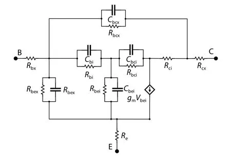
Fig.1.Complete small-signal equivalent circuit of HBT device including Cbi.gm=gm0e−jωτ.
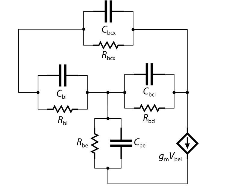
Fig.2.Small-signal equivalent circuit after de-embedding the extrinsic parameters.
3.Extraction procedure
3.1.Parasitic resistances
Since the parasitic resistancesRbx,RcandReare independent of the bias condition,we extract them under zero biasing conditions in this work.The calculation equations are given as follows[19]:Rbx=realRc=realandRe=realThe extractedRbx,RcandRefor the 2 × 20μm2HBT device are 6.186,2.561,and 5.526 Ω,respectively.The impedance matrixZmafter de-embeddingRbx,RcandRefrom the total two-portZ-parametersZcan be written as

ThroughY–Ztransformation,Ymcan also be expressed as

whereZbe=jωRbeCbe),Zbci=Rbci/Zbi=
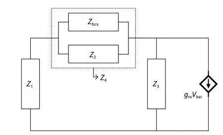
Fig.3.Final circuit after T-π transformation.
3.2.Intrinsic part parameters
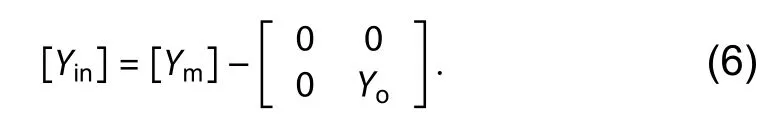
Once the parasitic resistances are known,the extraction of the intrinsic parameters can be carried out[20].The circuit is presented in Fig.2,and the admittance parameter of the intrinsic partYincan be written as
The circuit in Fig.2 can be converted to that in Fig.3 after T-π transformation[21]withThe parametersZ1,Z2,andZ3can be derived from Eq.(6) as follows
Combining Eqs.(6)–(9),Yincan also be represented byZ1,Z2,Z3,andZ4,which are expressed as[16]
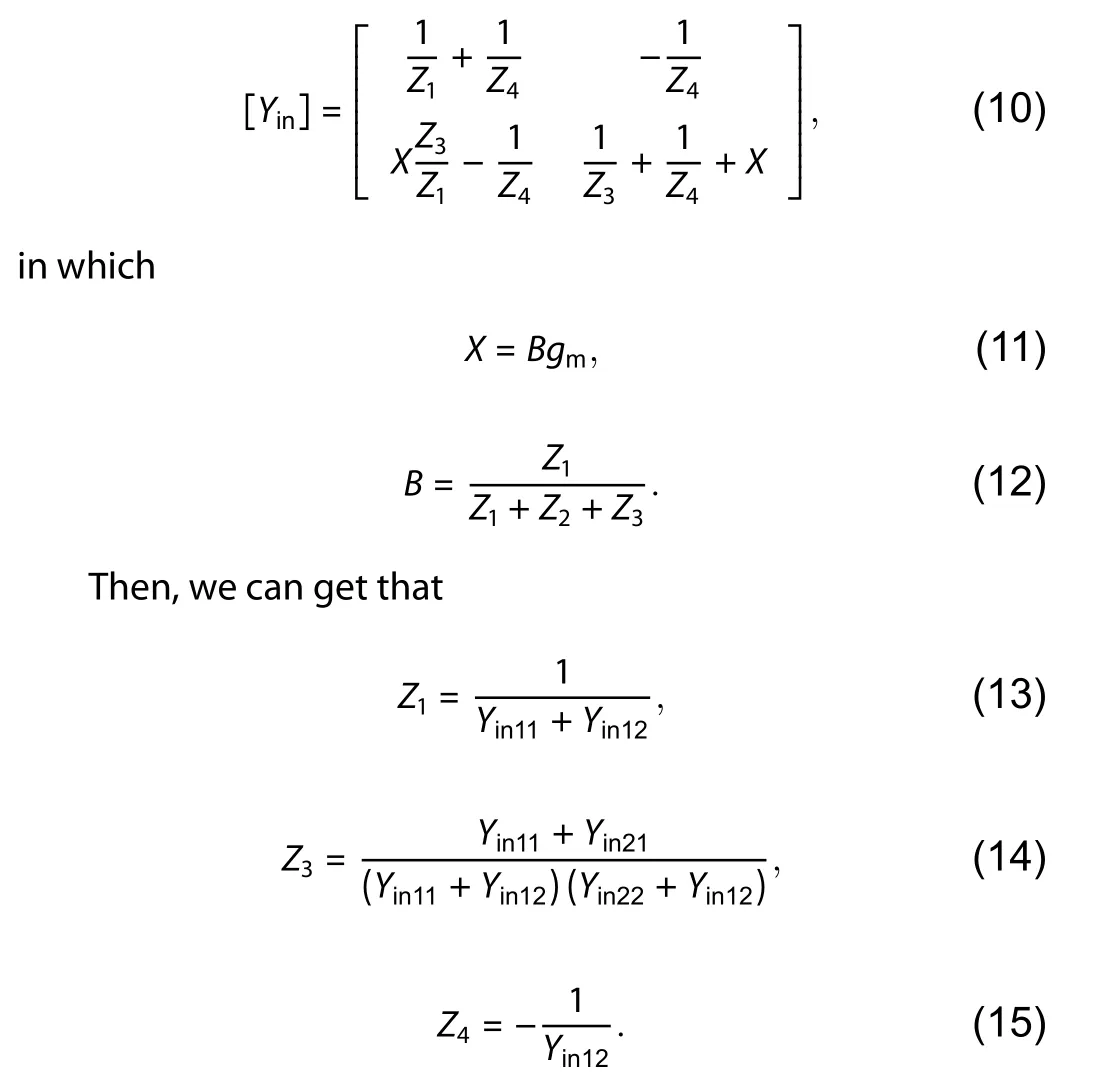
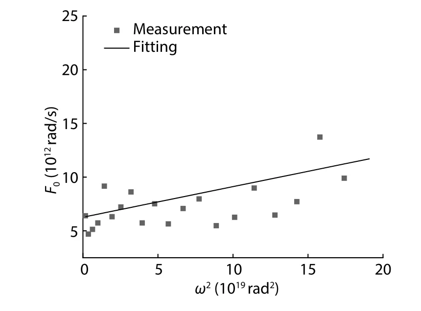
Fig.4.Frequency of F0versus ω2.
Based on the above relationship betweenYinandZ1,Z2,Z3,the extraction method reported in Ref.[18]is used to extract the parameters.From Eqs.(13) and (14),we can get

SinceZ1andZ3are given in Eqs.(13) and (14),theω2dependence ofF0can be easily plotted in Fig.4.ThenA0andB0can be determined.Tbiis defined as

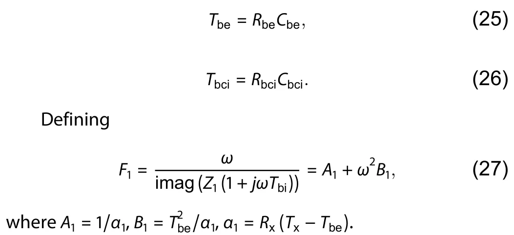
A1andB1can be obtained by using the straight-line fitting method.Then,Tbecan be determined as
Based on Eqs.(22) and (25),we can get

By extracting the real and imaginary parts ofF2,RxandTxcan be acquired from Eqs.(30) and (31).
Based on Eqs.(23) and (24),the expressions ofRxandRxTxcan be written as
Rbe,Rbican be determined from Eqs.(17),(18),(20),(28),(30),and (31).WhenRbeandRbiare obtained,Rbc,Cbc,CbeandCbican be obtained from Eqs.(17),(18),(25),and (26),respec-tively.In the end,the remaining parameters are written asCbcx=imaggm0andτare obtained from Eqs.(11) and (12):andτ=−phase(X/B/gm0)/ω.
4.Model verification
An GaAs HBT with 2μm emitter linewidth was used to validate the accuracy of the equivalent circuit.The adopted device was manufactured in a commercial foundry.The method in Section 3 is applied to extract the parameters of an HBT device with a 2 × 20μm2emitter-area under bias points of Bias1 (Vce=1 V,Ib=15μA),Bias2 (Vce=1 V,Ib=30μA) and Bias3 (Vce=3 V,Ib=17.5μA) in the frequency range from 100 MHz to 20 GHz.After extracting all parameters,the Keysight ICCAP software is used to optimize the extracted parameters to further reduce the error between the simulated and measured data.Here,the initial values ofArbe,ArcandAbexare set to 0.5 for optimization.Results of the extraction are compared with the extracted from the small-signal equivalent circuit of an AHBT (agilent heterojunction bipolar transistor) without consideringCbi.Table 1 shows the initial extraction and optimization results of the HBT device under Bias1 and Bias3.The comparisons of the real part and the imaginary part between the simulated and measuredS-parameters are plotted in Fig.5.The accuracy ofS-parameters versus frequency shows in Table 2.

Fig.5.S-parameters comparisons in the frequency range from 100 MHz to 20 GHz under the biasing condition:(a) Bias1 (Vce=1 V,Ib=15 μA),(b) Bias2 (Vce=1 V,Ib=30 μA),(c) Bias3 (Vce=3 V,Ib=17.5 μA).
Due to the inaccurate initial value of 0.5 for the partition parametersArc,Arbe,andAbexdefined before extraction,the extracted and optimized values ofRcx,Rci,Rbcx,Rbex,CbcxandCbexare slightly larger.From Fig.6,it can be seen that the proposed model withCbishows more accuracy than the one withoutCbi,which verifies the effectiveness of the introduced AC current crowding effect.
Fig.6 shows the decrease ofCbiwithIbandVce.Results present thatCbidecreases with increasingIbandVce,which is consistent with the result shown in Ref.[18].The experimental results show that the dependence betweenCbiand biases accords with the basic capacitance equation.
5.Conclusion
An improved small-signal equivalent circuit of the HBT device considering the AC current crowding effect is proposed in this paper.This effect is modeled as a parallel RC circuit withCbiandRbi.By comparing between the simulated and measuredS-parameters under three different biases,the results validate the reliability and availability of the proposed model and the developed extraction method.
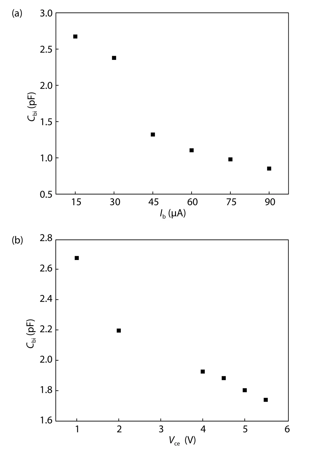
Fig.6.(a) Plot of Cbiversus Ib.(b) Plot of Cbiversus Vce.
Acknowledgements
This work was supported by the National Natural Science Foundation of China (Grant No.61934006)

Table 1. The initial extraction and optimization results of the HBT under Bias1 (Vce=1 V,Ib=15 μA) and Bias3 (Vce=3 V,Ib=17.5 μA).Error=|Extracted– Optimized|/ Extracted × 100%.
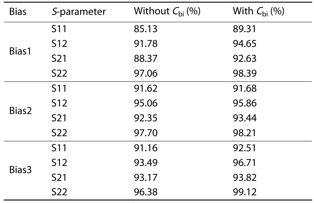
Table 2. The accuracy of S-parameters versus frequency.
 Journal of Semiconductors2021年5期
- Journal of Semiconductors的其它文章
- WO3 passivation layer-coated nanostructured TiO2:An efficient defect engineered photoelectrode for dye sensitized solar cell
- Compact SPAD pixels with fast and accurate photon counting in the analog domain
- Facile fabrication of heterostructure with p-BiOCl nanoflakes and n-ZnO thin film for UV photodetectors
- Morphology and crystalline property of an AlN single crystal grown on AlN seed
- A crossover from Efros–Shklovskii hopping to activated transport in a GaAs two-dimensional hole system at low temperatures
- Recent progress of physical failure analysis of GaN HEMTs