
Development of a seven-cell S-band standing-wave RF-deflecting cavity for Tsinghua Thomson scattering X-ray source
2021-05-06 03:20XianCaiLinHaoZhaJiaRuShiLiuYuanZhouShuangLiuJianGaoHuaiBiChen
Nuclear Science and Techniques 2021年4期
Xian-Cai Lin· Hao Zha· Jia-Ru Shi· Liu-Yuan Zhou·Shuang Liu· Jian Gao· Huai-Bi Chen
Abstract A 2856-MHz, π-mode, seven-cell standingwave deflecting cavity was designed and fabricated for bunch length measurement in Tsinghua Thomson scattering X-ray source (TTX) facility. This cavity was installed in the TTX and provided a deflecting voltage of 4.2 MV with an input power of 2.5 MW. Bunch length diagnoses of electron beams with energies up to 39 MeV have been performed.In this article,the RF design of the cavity using HFSS, fabrication, and RF test processes are reviewed.High-power operation with accelerated beams and calibration of the deflecting voltage are also presented.
Keywords Deflecting RF cavity·Standing wave·Bunchlength measurement · Thomson X-ray source
1 Introduction
The Tsinghua Thomson scattering X-ray source (TTX)was used as a tunable monochromatic X-ray source for advanced X-ray imaging experiments [1]. A photocathode RF electron gun provided 3-ps, 3.5-MeV Gaussian bunches, which were further accelerated to 50 MeV and compressed to 1 ps before interacting with the laser.During the experiments, it was crucial to diagnose the spatial and energy distribution of the bunch.A longitudinal distribution measuring system based on a three-cell deflecting cavity has been designed previously [2].Recently, an upgrade plan to boost the beam energy with X-band high gradient structures [3] and provide greater than 5-MV deflecting voltage with 4-MW power input was proposed,and a seven-cell standing-wave-deflecting cavity(SDC) was developed and fabricated to provide a higher deflecting voltage and better measurement accuracy.
When the deflecting cavity operates, the electron bunches enter the cavity center at zero phase. A deflecting force, approximately linear to the longitudinal location,acts on the bunch.As a result,the longitudinal distribution of the bunch is converted to a transverse distribution on the screen after drifting some distance.From the perspective of beam transmission, the bunch undergoes a linear shear transformation in the system. Therefore, the RF-deflecting cavity provides a direct method to measure the bunch length, as well as high resolution.
In recent years,many deflecting cavities for bunch-length measurement have been designed and fabricated, including traveling-wave-deflecting structures(TDSs)and SDCs.Various deflecting structures have been reported,such as L-band TDS at PITZ[4];L-band SDC for the Cornell ERL injector[5];S-band TDS at SLAC(LOLA IV[6,7])and IHEP[8,9];S-band SDC at FERMI SPARC [10], Tsinghua University[11],and Waseda University[12];C-band TDS at Spring 8 for X-FEL (RAIDEN [13, 14]) and at PSI for SwissFEL [15];C-band SDC at Tsinghua University[16,17];X-band TDS at SLACforLCLS[18,19],atShanghaiforSXFEL[20,21],and atPSIfor SwissFEL(PolariXTDS[22,23]);and X-bandSDC at UCLA [24]. Generally, a higher operation frequency can provide better measurement accuracy. In our design, a frequency of 2856 MHz was chosen based on the existing RF system in TTX. Although TDSs can provide a stronger deflecting voltage, an SDC is selected because it is more compact and efficient. Increasing the cell number could enhance the deflecting ability of the cavity; we chose 7 to provide a targeted deflecting voltage.
This paper presents an intact process for designing and testing a seven-cell SDC.The theory of SDCs is reviewed,and a simple and quick method is used to optimize a multicell SDC working in π mode.The influence of the end-cell length on the transverse shunt impedance is also explored.RF tests after fabrication are shown,including the unloaded Q values,external Q values,and field distribution.Finally,high-power operation with accelerated beams and calibration,as well as their underlying principles,is demonstrated.
2 Basic properties of SDCs for bunch-length measurement
From the perspective of how the microwave propagates inside the cavity, deflecting cavities are divided into traveling- and standing-wave structures.Both have advantages and disadvantages. For traveling-wave structures, there is negligible power reflection from the structure, and the structure can be stacked until very long. A formula can be used to estimate the deflecting voltage Vdefversus input power P0and structure length L for the S-band disk-loaded traveling structure [7].

For standing-wave structures, because the microwave is trapped and coherently stacked inside the cavity, less power is needed to yield the same field level as that of the traveling-wave structure. A similar formula can be concluded from Ref. [11] for an S-band disk-loaded standingwave structure.

The disadvantage of the standing-wave structure is that power is reflected during the filling process, and a circulator is needed to direct this power to the load to avoid influencing the power source. Furthermore, to avoid mode aggregation, the standing-wave structure cannot be too long.According to the upgrade plan to provide more than 5 MV of deflecting voltage with a 4-MW input, the shortest structure lengths using Eqs. (1) and (2) are 1.6 m and 0.34 m for traveling- and standing-wave structures,respectively. The latter is only one-fifth that of the former.Considering the existing room for the TTX beamline and moderate input power for the deflecting cavity,a standingwave structure was adopted.The SDC operates in the TM110-like mode.For an ideal cylindrical cavity, there is only a transverse magnetic field along the z axis. In this study, we set the direction of the transverse magnetic field as the x axis. With this convention,the charged particles moving along the z axis suffer a deflecting force in the y direction. Owing to the beam tunnel at a realistic cavity for charged particles to go through as well as coupling between cells, there is an Eycomponent in the z axis to satisfy the boundary condition.The field distribution in a single cell operating in the TM110-like mode is shown in Fig. 1.For a particle moving at a velocity near the speed of light,its momentum change approximately equals the energy change divided by c, i.e.,Δp=∫Fdt ≈∫Fdz/c=eV/c. Therefore, the voltage is used to describe the momentum change. The transverse voltage can be calculated as the integration of the electric and magnetic fields along z axis, as shown in Eq. (3).
where φ is the phase of the microwave when the particle arrives at z = 0. ~Eyand ~Hxare the complex electric and magnetic fields, respectively, and η is the free-space wave impedance. Re{ } represents the real components. The concept of deflecting voltage is used to describe the maximum transverse voltage a charged particle can gain,which can be calculated as
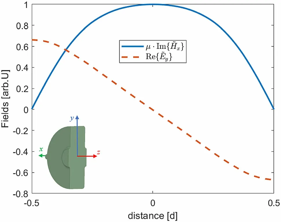
Fig.1 Magnetic and electric fields of a single cell in a standing-wave cavity
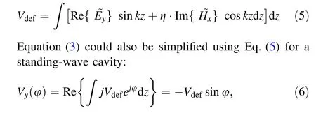
where || represents the magnitude of the enclosed value.For the standing wave, ~Eyand ~Hxhave a 90° difference in phase. Therefore, an appropriate phase can be selected to yield ~Ey=Re{ ~Ey} , ~Hx=j·Im{ ~Hx} .It is noted that the results from simulation software, such as HFSS, have this form. Considering the symmetry of fields in a single cell(z = 0 is set at the middle of the cell),∫Re{ ~Ey} cos kzdz=∫Im{ ~Hx} sin kzdz=0,,where k is the wavenumber of the microwave. Therefore, Eq. (4) can be simplified for a standing-wave cavity as Eq. (5).
It should be noted that Eq. (5) could be simplified further with the Panofsky–Wenzel theorem by integrating longitudinal electric field off z axis [2], but Eq. (5) could provide more physical information. For example, the calculation using the data shown in Fig. 1 with Eq. (5)shows that both the magnetic and electric fields attributed to the deflecting voltage accounted for 64% and 36%,respectively.
For deflecting cavities used to measure bunch lengths,the center of the bunch experiences zero transverse voltage,which means that the bunch center arrives at the cavity center at phase φ=0. Therefore, a charged particle at a distance Δz from the center would arrive at the cavity center at a phase φ=-kΔz. Its transverse voltage can be calculated by

which shows that a force approximately linear to the longitudinal location of the particle is applied to the bunch.The deflecting voltage represents the ability to transform the longitudinal location of the bunch to the transverse location. The original three-cell deflecting cavity at TTX can provide a 3.4-MV deflecting voltage with a 4-MW input [2]. The goal of the upgrade plan is to increase the deflecting voltage to 5 MV. According to the definition of transverse shunt impedance,
This is also the derivation of Eq. (2). Because R⊥/L remains almost the same with different cell numbers for identical cell shapes, the deflecting voltage with the same input power is nearly proportional to the square root of the cell number.In our design,this number is chosen to be 7 to provide an approximately 5.2-MV deflecting voltage with an input power of 4 MW.
3 RF design of seven-cell SDC
The cavity shape is a disk-loaded structure. The polarization degenerated mode of the TM110 mode is separated by a pair of cylindrical slots on the sidewall of the cells.The magnitudes of the electric and magnetic fields of the working mode and degenerated polarized mode at the xy plane(z = 0)are shown in Fig. 2.In this figure,(a,b)show that the polarization of the working mode is on the y axis,while the degenerated mode is at the x axis.(c,d)show that the working mode has little field at the slot, while the degenerated mode has a comparatively strong magnetic field at it. According to perturbation theory, the existence of slots reduces the frequency of the degenerated mode,while it has little influence on the working mode. The frequencies of these two modes versus the slot radius are shown in Fig. 2e. The center of the slot was located at the side faces of the cavity.A quadratic function is appropriate for describing the relationship because the frequency perturbation amount is nearly proportional to the perturbation volume. In our model, the slot radius is 5 mm, and the frequency of degenerated mode is 6.5 MHz lower than the working mode, which is larger than the frequency bandwidth of the working mode and variation of the microwave power source and therefore adequate for operation. It should be noted that slots do not need to be set at the center cell because the power coupler can separate the degenerated mode.
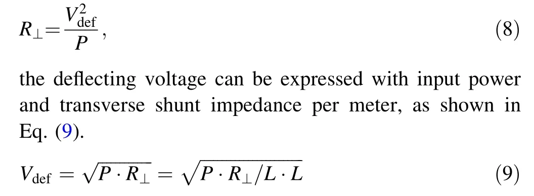
The design goal of an SDC is to settle its eigenmode frequency and optimize its magnetic field distribution along the z axis,as the magnetic field provides a major part of the deflecting voltage. The radius of each cell was adjusted to achieve this goal.For an n-cell cavity,this is an n-dimensional optimization problem. The symmetry of the cavity means that cells can be divided into three types:the center cell with the coupler, the inner cells, and the end cells with beam tunnels,corresponding to part 1—in Fig. 3.Therefore, this n-dimensional problem is simplified to a three-dimensional one. Furthermore, because the cavity works in the π mode,each cell can be separated as a single cavity with a perfect H boundary (the transverse magnetic field is zero) at the intersection plane. The optimization of each type of cell can be performed individually to make them work at the designed frequency. After combining these three parts, only a precise adjustment was needed to generate a flat field distribution. The parameters of the cavity after optimization are listed in Table 1, where a is the radius of the beam pipe as well as the iris, biis the radius of each cell, diis the cell length, and t is the thickness of the disk,as shown in Fig. 3.The subscript i is the index of the cells, numbered 1–7 from left to right.

Fig.2 (Color online)a Electric field amplitude of the working mode at xy plane; b electric field amplitude of the degenerated polarized mode; c magnetic field amplitude of the working mode; d magnetic field amplitude of the degenerated polarized mode;e frequency of the working mode and the polarized degenerated polarized mode versus slot radius. The center of the slot is located at the side faces of the cavity
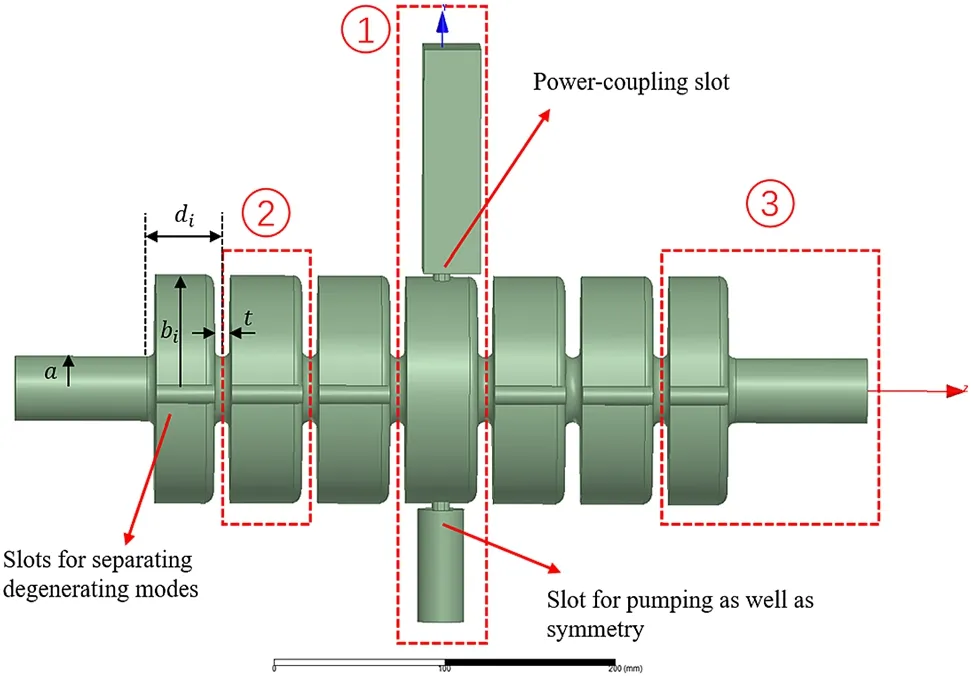
Fig.3 (Color online)3D model of the seven-cell deflecting cavity in HFSS

Table 1 Parameters of the seven-cell deflecting cavity
The RF power was fed into the cavity with a BJ-32 (or WR-284)waveguide through a coupling slot.The coupling factor of the cavity was set to 1.1,with the experience that the Q0value after fabrication was approximately 85% the simulated value [25]. According to the definition, the coupling factor was set to 1.1 × 7 in the isolated center cell model. The calculation and optimization process was accomplished using high-frequency simulation software[26]. Two methods were utilized: the modal solution,where power is fed from the waveguide and the coupling factor is calculated from the S11 parameter; and the eigenmode solution, where the absorption material is placed at the end of the waveguide.The relative difference between the two solutions is less than 1 × 10⁻³, whereas the latter requires less CPU time.The RF parameters of the cavity are listed in Table 2. The final size of the coupling slot was 28.66 × 10.00 mm2. An identical slot was placed at the other side of the center cell for pumping, as well as for symmetry, as shown in Fig. 3.
The wideband frequency response of the cavity calculated in the HFSS,as well as the identification of modes,is shown in Fig. 4. Because the power is fed through themiddle cell, only the symmetric mode, i.e., π mode, 2π/3 mode, π/3 mode, and 0 mode, is activated. The magnetic field patterns at the yz plane (x = 0) are also plotted in Fig. 4.The nonsymmetric modes of this cavity,i.e.,the 5π/6, π/2, and π/6 modes, are suppressed. The nearest mode,2π/3 mode, is 13 MHz from the working mode, which is adequate for practical operation.

Table 2 Simulation results of the seven-cell deflecting cavity
Owing to the large apertures of the deflecting cavity,there was obvious field leakage in the end cells. In other words, there was a long tail at the end of the cavity in the magnetic field distribution along the z axis. This could be compensated by shrinking the iris at the two ends. However, considering that the bunch’s transverse size became larger after deflection, this idea was abandoned. Instead,shortening the length of the cells at the two ends was adopted. To study the influence of end-cell length, the transverse shunt impedance and transverse shunt impedance per meter versus end-cell length were calculated in HFSS, as shown in Fig. 5a. In each end-cell length case,the cell radius and coupler hole were adjusted to maintain the working frequency, field flatness, and coupling factor.Two cases of end-cell lengths of 45 and 52.52 mm were selected to plot their magnetic field distribution, as shown in Fig. 5b.According to Fig. 5a,b,although the full width at half maximum(FWHM)at the end cell is shortened with decreasing end-cell length, the shunt impedance is decreased. This could be explained by two effects on the shunt impedance when shortening the end-cell length.First,less energy was needed for the end cells,which could lead to higher power allocation in other cells.This led to an increase in the field distribution. Second, the location of Hmaxat the end cell moved and deviated from its best location to synchronize with the bunch. In other words,when the particle arrived at the location of Hmax,the fields in the cavity were not at their maximum moments, which led to a decrease in shunt impedance. The simulation results show that the second effect outweighs the first effect. As a result, shortening the end cell leads to a slight drop in the transverse shunt impedance. However,because of the decrease in length, the shunt impedance per meter increased.As a compromise between the cavity length and deflecting voltage, an end-cell length of 45 mm was chosen, where the shunt impedance per meter was the maximum value.
Fig. 4 (Color online) S11 curve of the seven-cell deflecting cavity and magnetic field plot of different modes at yz plane (x = 0)
4 Cavity fabrication and RF measurement
The final CAD model for fabrication is shown in Fig. 6.A series of cells was formed by stacking the bowl cavities.This bowl cavity is similar to the normal cavity as an accelerating structure, except for two cylindrical slots in the x direction for polarized mode separation. Because the bowl cavity is not circularly symmetric, alignment slots were notched outside for assembly. A pair of tuning holes was made for each bowl cavity on the outer wall for tuning after brazing and during operation. Tuning holes were placed in the y direction, where the power coupler was located, because the frequency sensitivity was the largest there. On the center cell, owing to the existence of the power coupler, four tuning holes were placed at an angle from the y axis. The power-feeding waveguide used an SLAC-type female flange, whereas the beam pipe and pumping port used CF-35 flanges. The feedthrough was placed in the vacuum pipe for an RF pickup to measure the signal inside the cavity. Four cooling pipes were welded near the alignment slots.The length of the whole model in the z direction, including beam pipes and flanges, was 431.35 mm.where t0is the operation temperature, t1is the environmental temperature of the microwave measurement, εris the relative permittivity of air,and α is the linear expansion coefficient of copper. The measurement data before brazing, after tuning compared with the designed value, are shown in Table 3. The Q0value after fabrication was only approximately 2% less than the design value. The comparison of the measured and simulated S11 curves, displayed in Fig. 7, also shows good consistency between the simulation and fabrication.
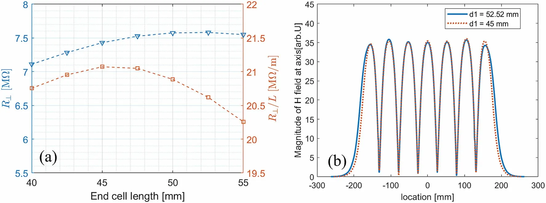
Fig. 5 (Color online) a Transverse shunt impedance and transverse shunt impedance per meter versus end-cell length; b comparison of field distribution with two different end-cell length cases at 52.52 mm and 45 mm

Fig. 6 (Color online) CAD model for fabrication
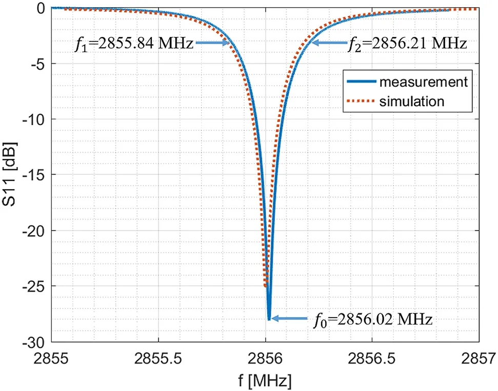
Fig.7 Measured(solid line)and simulated S11(dotted line)curve of seven-cell cavity
The field distribution was measured using the bead-pull method, as shown in Fig. 8. The cavity was placed vertically and connected to a vector network analyzer through a coaxial-to-waveguide adapter. The perturbation bead was made from a copper sheet and wound with nylon wires.The motion of the bead was controlled using a stepping motor.
According to the perturbation theorem, the relationship between the frequency perturbation and field amplitude is given by Eq. (11) [16].

where α and β are coefficients determined by the shape of the bead and the material attribute. At the location where the magnetic field reaches its maximum,the electric field is zero. Therefore, the maximum frequency shift representsthe maximum magnetic field. Only the relative field magnitude was considered in the test.Owing to the polarization of the working mode, the rotation of the bead changes the coefficients and causes errors in field measurements. A two-line bead-pull method was proposed in Ref. [16] and used in this experiment to prevent rotation of the bead.The bead was wound with two nylon wires,and a special pulley was fabricated to separate these two lines, as shown in Fig. 8.
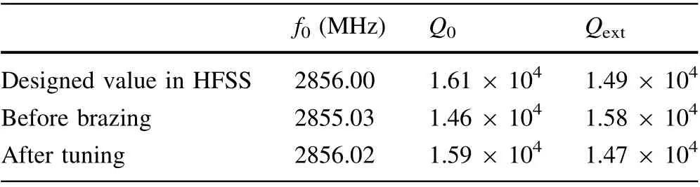
Table 3 Frequency, unloaded quality factor, and external quality factor of different stages

Fig. 8 (Color online) Field distribution measurement platform
After brazing, the frequency was 500 kHz lower than the designed value, and the field distribution was not flat.The frequency and field distribution were tuned simultaneously to avoid repeatedly pushing and pulling the tuning hole. When tuning, pushing the hole of one cell would increase the frequency of the working mode as well as the field in this cell decline. The motion of the bead was controlled using a stepping motor. However, during the tuning process,it was suggested to control it manually and only collect the maximum frequency shift for each cell.This could reduce the time to perform the entire field measurement. The results of the bead-pull measurements before and after tuning are shown in Fig. 9.The frequency change Δf was normalized to that of the center cells, Δf0.In the field distribution, there are seven crests above the baseline, which indicate the peak magnetic field in the middle of the cells, and six valleys below the baseline,which indicate the peak electric field at the iris location along the axis.Before tuning,the relative frequency change indicated that the magnetic field varied from 1.0 to 1.5.Because the magnitude of the field is proportional to the square root of the frequency change, the maximum variation of the cell-to-cell magnetic field before tuning was approximately 25%. After tuning, the relative frequency change varied from 0.9 to 1.1, and the maximum variation in the cell-to-cell magnetic field after tuning dropped to approximately 6%.
5 High-power operation with accelerated beam
After fabrication and tuning, this deflecting cavity was installed at the TTX beamline. A photograph of the deflecting cavity at the platform is shown in Fig. 10a. The layout of the RF system in the TTX is shown in Fig. 10b.The entire RF system is fed by a 2856-MHz klystron,which can provide a 2-μs, 40-MW high-power microwave pulse with a repetition rate of 10 Hz. The power from the klystron is first divided by a 5-dB directional coupler.Then, a 13-MW pulse travels to the photocathode RF gun,which is triggered by a laser to provide a 3-MeV highquality electron beam at its exit. The remaining 27-MW pulse is further divided by a 10-dB directional coupler. A 24-MW pulse travels to the main acceleration section, a 3-m S-band traveling structure,which can boost the bunch to approximately 50 MeV. The remaining 2.7-MW power goes through a circulator to feed the deflecting cavity. It should be noted that all these power values were calculated without transmission loss. Attenuators, phase shifters, and dry loads are also used to adjust the microwave power,control the microwave phase, and absorb the residual power. Directional couplers are placed before each RF structure to measure the input and output pulses. Before operation, the cavity is subjected to an 18-h conditioning process. The input power of the cavity reached 2.5 MW,which is the maximum value our RF system can provide.
As shown in Fig. 10b, the electron bunch generated by the photocathode was accelerated by the 3-m structure.Then, the accelerated bunch entered the deflecting cavity.When the deflecting cavity is switched on,a force linear to the offset of the electron, relative to the bunch center, acts on the bunch. The relative momentum change in the y direction can be calculated by Eq. (12).

where p is the momentum of the bunch,W is the energy of the bunch,and Δz is the particle’s z location relative to the bunch center.After exiting the deflecting cavity,the bunch drifts for a distance of D before colliding with the screen.The relationship between the y position of a particle at the location of the screen and its original position is

Fig. 9 a Bead-pull measurement result of the seven-cell deflecting cavity before tuning, b bead-pull measurement result of the seven-cell deflecting cavity after tuning
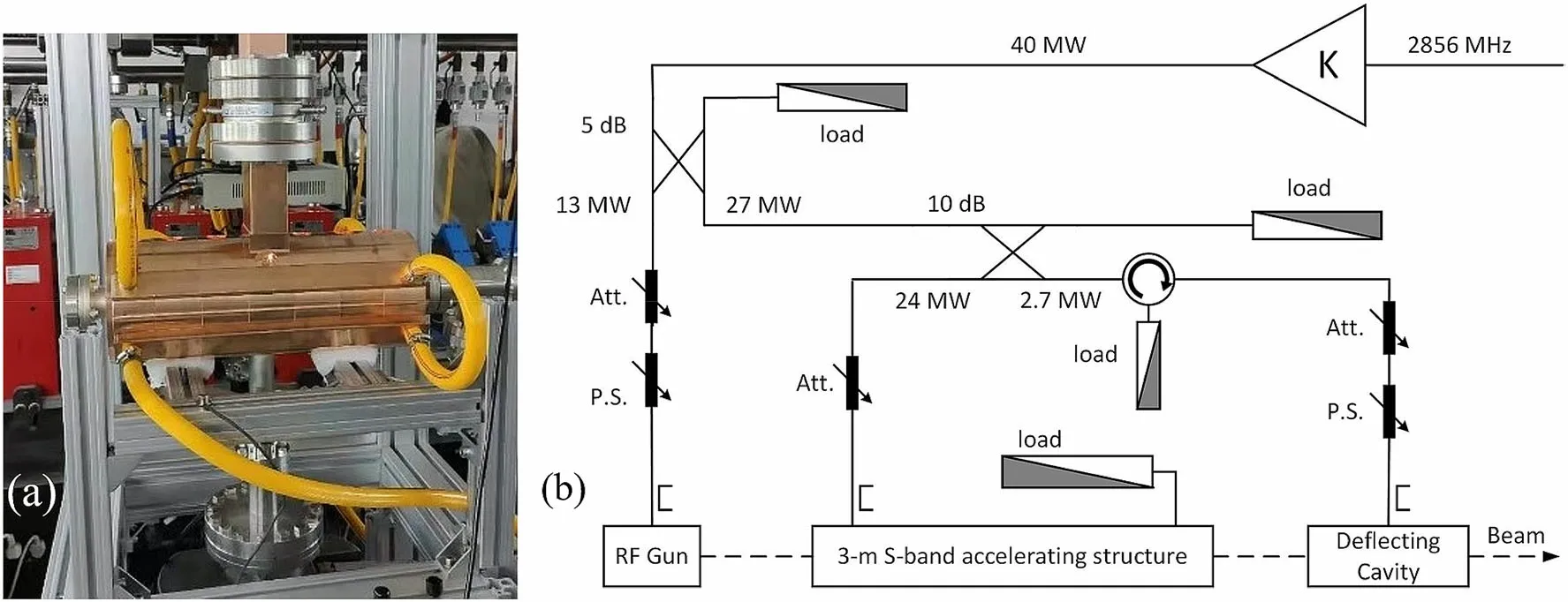
Fig. 10 (Color online) a Photograph of the deflecting cavity at the platform; b RF power-feeding system of the TTX. Att. and P.S. stand for attenuator and phase shifter, respectively. The power value was calculated without transmission loss
In this experiment at the TTX beamline,40-pC bunches emitted from the photocathode cavity were accelerated to 39 MeV, which was measured using a magnetic analyzer.Bunch projections were collected onscreen as the deflecting cavity was switched off and on. When the deflecting cavity was switched off, the bunch had a small transverse size, leaving a small beam spot on the screen, as shown in Fig. 11a.The transverse RMS bunch size in the y direction was σy,0=1.17 mm. When the deflecting cavity was switched on,the longitudinal distribution was converted to a transverse distribution,and the beam spot became a long strip,as shown in Fig. 11b.The transverse RMS bunch size after deflection in the y direction was σy=5.50 mm.
Before using Eq. (15) to calculate the longitudinal bunch length, Vdefmust be known or measured, but it can also be calculated using the measured input power and the simulated transverse shunt impedance.In the experiment,it was measured by calibrating the deflecting cavity. The calibration process involves shifting the input microwavephase and measuring the displacement distance of the bunch center. When the phase is offset, the bunch center deviates from its zero-phase location.According to Eq. (6),the deflecting voltage of the bunch center becomes Vy(Δφ )=-Vdefsin Δφ ≈-VdefΔφ, where Δφ is the phase shift of the input microwave. It should be noted that this is equivalent to offsetting the bunch center at a distance Δz=-Δφ/k.The relation between the displacement distance of bunch center and the offset phase is

Fig. 11 (Color online) a Bunch projection with the deflecting cavity switched off; b bunch projection with the deflecting cavity switched on

where Δy is the displacement distance of the bunch center,and Δφ is the offset phase controlled by the phase shifter.The calibration coefficient eVdefD/W can be used directly to calculate the longitudinal bunch length using Eq. (15).In our experiment, the calibration coefficient was used to calculate the deflecting voltage and transverse shunt impedance, which were compared with the simulated values.
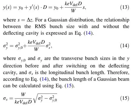
The projection of the bunches with and without phase offset during calibration is shown in Fig. 12.The blue solid line is the outline of the bunch that enters the deflecting cavity at the zero phase.The green dotted line is the outline of a bunch that enters the cavity at a 1° phase offset. The distance between their bunch centers in the y direction is 4.4 mm. Therefore, according to Eq. (16), the calibration coefficient was eVdefD/W =0.253 m/rad. The measured bunch length of the beam σsin this experiment is 0.354 mm, or 1.18 ps, using this calibration result. The parameters of the measurement condition and calibration results are listed in Table 4.The measured transverse shunt impedance is 7.1 MΩ/m. It should be noted that this is a preliminary experiment using two RF phases.Experiments including more phases and error analyses will be performed in the future.
Fig.12 (Color online)Projection of bunches without and with phase offset during calibration. The blue solid line is the outline of the bunch that enters the deflecting cavity at zero phase.The green dotted line is the outline of a bunch that enters the cavity at a 1°phase offset.The distance between the bunch centers in the y direction is 4.4 mm
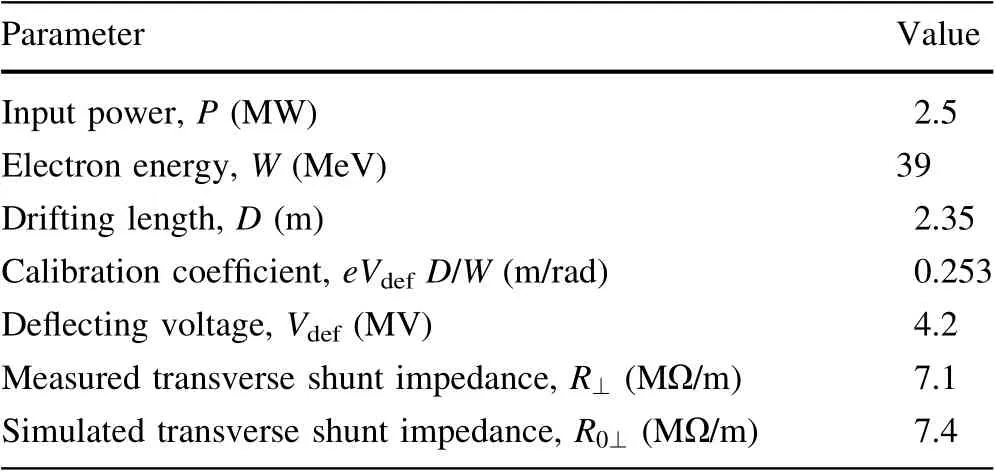
Table 4 Bunch-length measurement condition and calibration results
6 Conclusion
This paper presents the design, RF testing, and bunchlength measurement of a 2856-MHz, π-mode, seven-cell SDC in the TTX platform. The theory of the SDC and its bunch-length measurement and calibration have been reviewed. Compared with the TDS, the SDC is more compact,with its length only one-fifth that of the traveling wave,in our case.A simple and quick method was used to optimize the multicell SDC working in π mode. The transverse shunt impedance per meter was optimized by adjusting the end-cell length,which can guide the design of a multicell deflecting cavity. After fabrication and tuning,the parameters of the cavity correspond well to the simulation results in the HFSS.
This cavity was installed in a TTX and provided a deflecting voltage of 4.2 MV with an input power of 2.5 MW. Bunch-length diagnosis of electron beams with an energy of 39 MeV was performed. In the near future,this cavity will be used for bunch-length measurement in a new beamline in Tsinghua, which will generate terahertz radiation with a laser-modulated electron bunch for research.
Author contributionsAll authors contributed to the study conception and design. Material preparation, data collection and analysis were performed by Xian-Cai Lin, Liu-Yuan Zhou, Jian Gao, and Shuang Liu.The first draft of the manuscript was written by Xian-Cai Lin, and all authors commented on previous versions of the manuscript. All authors read and approved the final manuscript.
 Nuclear Science and Techniques2021年4期
- Nuclear Science and Techniques的其它文章
- Charge resolution in the isochronous mass spectrometry and the mass of 51Co
- Design, fabrication, and cold test of an S-band high-gradient accelerating structure for compact proton therapy facility
- Simulation of proton-neutron collisions in inverse kinematics and its possible application
- Sinogram denoising via attention residual dense convolutional neural network for low-dose computed tomography
- Secondary and activated X(γ)radiation of SPHIC particle therapy facility
- Analysis of influencing factors on the method for determining boron concentration and dose through dual prompt gamma detection