P hotonic devices based on thin-film lithium niobate on insulator
Shuai Yuan, Changran Hu, An Pan, Yuedi Ding, Xuanhao Wang, Zhicheng Qu, Junjie Wei, Yuheng Liu,Cheng Zeng, and Jinsong Xia
Wuhan National Laboratory for Optoelectronics, Huazhong University of Science and Technology, Wuhan 430074, China
Abstract: Lithium niobate on insulator (LNOI) is rising as one of the most promising platforms for integrated photonics due to the high-index-contrast and excellent material properties of lithium niobate, such as wideband transparency from visible to mid-infrared, large electro-optic, piezoelectric, and second-order harmonic coefficients. The fast-developing micro- and nanostructuring techniques on LNOI have enabled various structure, devices, systems, and applications. In this contribution, we review the latest developments in this platform, including ultra-high speed electro-optic modulators, optical frequency combs,opto-electro-mechanical system on chip, second-harmonic generation in periodically poled LN waveguides, and efficient edge coupling for LNOI.
Key words: thin-film lithium niobate; modulator; PPLN; edge coupler
1.Introduction
Compared to traditional microwave links, microwave photonic links have a series of advantages such as instantaneous broadband processing capability, light weight, low loss,anti-electromagnetic interference, etc., and in recent years,they have been widely used in radar and other fields.However, most of the current microwave photonic systems are built using discrete optoelectronic components, so there are shortcomings such as low integration, high link loss, large noise coefficient, which seriously hinders the performance of microwave photonic technology. So there is an urgent need to enable the on-chip integration of microwave photonic systems[1].
Research of integrated photonics has progressed rapidly in the last decade. Researchers have built low-loss optical waveguides, lasers, modulators, detectors on materials such as silicon[2,3]and indium phosphide[4], and have achieved monolithic integration of multifunctional devices. The advantages of these integrated photonic chips are small footprint,high integration, low power consumption, and high gain due to reduced link loss, while allowing for more complex functions. However, materials such as silicon and indium phosphide have some drawbacks of their own, which make the above-mentioned research results unable to meet the requirements for the integration of microwave photonic systems.For example, electro-optical modulators based on silicon-on-insulator (SOI) and InP materials have temperature sensitivity,nonlinear distortion, two-photon absorption and other shortcomings[5], which are not suitable for microwave photonic systems. Therefore, there is an urgent need for researchers to find a new integration platform for broadband optoelectronic devices.
Lithium niobate on insulator (LNOI) materials are structurally similar to SOI materials. It can be divided into three layers, the substrate layer (silicon), a low refractive index oxide layer (silicon dioxide) and a high refractive index device layer (lithium niobate film). Due to the high refractive index contrast between lithium niobate and silicon dioxide, thin-film lithium niobate waveguides allow for a strong limitation of the optical field and tight waveguide bending radii, thereby reducing the size of photonic devices. We believe that LNOI materials have the following advantages over silicon, indium phosphorus, silicon oxide, and silicon nitride materials.
(1) Due to the large refractive index difference between the waveguide core and the outer cladding, the dimensions of both SOI and InP waveguides are small, and there is a significant overlap between the inner mode and the waveguide sidewalls, which makes it difficult to reduce the scattering loss of light waves due to rough sidewalls.
(2) Si3N4and SiO2materials lack intrinsic electro-optical effects, and can only achieve modulation of optical phase through thermal-optical effects, so the optical switching speed realized on Si3N4and SiO2platform is slow (about submillisecond magnitude) with high power consumption.
(3) The refractive index contrast of the LNOI platform is high, which allows the construction of low-loss waveguides.The electro-optical effect of lithium niobate has femtosecond response speed, enabling ultra-wideband electro-optical modulators[6]. Thin film lithium niobate also has a high nonlinear coefficient, which can be used for coherent light source generation[7]and optical parameter amplification[8].

Fig. 1. (Color online) The structure of the EO modulator made by Wang et al.[6].

Fig. 2. (Color online) (a) Optical image of the modulators on the chip fabricated in our group. (b) SEM image of the electrode of the modulator.(c) SEM image of the cross section of the modulator’s waveguide. (d) SEM image of the area where the electrode stepping over the waveguide.
LNOI inherits the excellent material and optical properties of the bulk lithium niobate, and has the ability to integrate photonic devices similar to the SOI platform, which is very suitable for building a new generation of broadband,low-power microwave photonic RF front-end chips. In the second part, we will introduce the broadband electro-optical modulator, which is one of the core devices in the microwave photonic system. Its key parameters such as bandwidth, insertion loss, half-wave voltage and extinction ratio directly affect the performance of the whole microwave photonic link. In the third part, we will introduce the optical comb devices, including the electro-optical comb and the Kerr optical comb. In the fourth part, we will introduce how the coupling of multi-physics fields such as optical, acoustic, and electric fields can be achieved on thin-film lithium niobate chips,and discuss the possible applications. In the fifth part, we will introduce the thin film periodically poled lithium niobate(PPLN) waveguides, which play an important role in second harmonic generation (SHG), all-optical wavelength conversion and optical parametric amplification (OPA). In the sixth part, we will introduce the efficient coupling between thinfilm lithium niobate waveguides and optical fibers, which is one of the prerequisites for the practical application of thinfilm lithium niobate devices.
2.High-speed lithium niobate modulator
As early as 2007, Guarinoas et al. shows the electro-optically tunable microring resonators in thin film lithium niobate[9]. Different kinds of modulators on lithium niobate have been intensively studied[10-12]. But it was not until 2018 that Wang et al. of Harvard University demonstrates a very high performance EO modulator based on LNOI in 2018[6], as is shown in Fig. 1. A modulator with the electro-optic bandwidths over 100 GHz as well as the relatively low driving voltage is realized. This research shows the high-speed application potential of LNOI. In addition, an integration of a Kerr frequency comb, a tunable filter and a modulator has been shown in a single LNOI chip[13]. The combination of the Pockels effect and the Kerr effect reveals the prospect of the multichannel transmitting module based on LNOI. A lithium niobate photonic-crystal electro-optic modulator which features a small footprint is made by Li et al.[14]. So, the higher level of integration of LNOI chips is also promised. Besides,He et al. of Sun Yat-sen University shows a hybrid silicon and lithium niobate modulator which proves the compatibility between silicon and LNOI[15]. This report implies that several mature Si-based devices are available when we construct the LNOI-based photonic integrated circuit (PIC). It provides more flexibility of the PIC design. Then Xu et al. of the same group realize the coherent optical modulating on a single LNOI chip[16].
In our group, the modulator is fabricated on a commercially available X-cut LNOI substrate (NANOLN) through a standard semiconductor process. The optical and the scanning electron microscope (SEM) images of the modulators are shown in Fig. 2.
The transmission spectrum and the driving voltage test result of the modulator is indicated in Fig. 3(a). The measured free space range is about 3 nm and the VπL is about 2.75 V·cm. The measured EO response of the modulator are shown in Fig. 3(b), which exhibits a 3 dB EO bandwidth of about 40 GHz. In addition, the insertion loss of the whole device is about 3 dB when measured with high numerical aperture fiber (HNAF) and refractive index matching liquid.
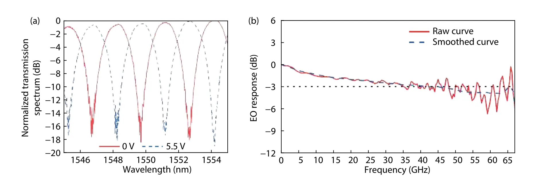
Fig. 3. (Color online) (a) The transmission spectrum of the modulator with and without the voltage applied. (b) The measured EO response of the modulator.
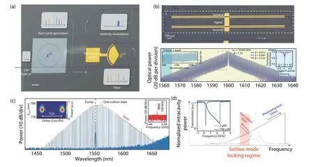
Fig. 4. (Color online) (a) Monolithic integrated photonic circuit for frequency comb generation and manipulation[13]. (b) Integrated EO comb generator[22]. (c) LN microring mode-locked Kerr solitons. (d) Photorefractive and optical Kerr effect[7].
3.Optical frequency comb
Micro-resonator Kerr optical frequency combs characterized by discrete and equally spaced frequencies and high-repetition rate has provided miniaturised solutions for many applications, such as optical metrology, pulse shaping, light detection and ranging (LiDAR) and sources for quantum entanglement[17,18].
At present, almost all on-chip micro-resonator Kerr frequency comb generators rely on Kerr (third-order, χ(3)) nonlinear optical process. A continuous-wave laser source is injected in an optical micro-resonator which has a large Kerr nonlinear coefficient and low optical loss. They have been realized in various material platforms, including crystalline fluorides,Si3N4, SiO2, diamond, aluminium-gallium arsenide (AlGaAs), aluminium nitride (AlN) and Gallium phosphide (GaP)[18,19].
LN has been widely used in nonlinear optics, as it simultaneously possesses electro-optic (χ(2)= 30 pm/V) and Kerr (χ(3)=1.6 × 10⁻²¹m2/V2) nonlinearities[20]. Thin-film LNOI, which offers attractive material properties of LN and stronger optical confinement, has become commercially available. In the past,the main challenge for the monolithic approach relying on direct etching of LN often suffers from a relatively high propagation loss. Recently, Wang Cheng et al. has overcome the difficulty of fabricating and realized ultra-low loss waveguide with propagation losses as low as 2.7 dB/m and microring resonators with quality factors up to 107[21]. This further promotes the development of on-chip optical frequency combs.Represented by the research teams of Harvard University and University of Rochester, they have successfully implemented Kerr frequency comb generation and modulation[13], electrooptical combs[22]and optical soliton[7]on LNOI.
As we all know, the above-mentioned platforms that have realized the generation of optical frequency comb such as silicon nitride usually possess large χ(3)but near zero χ(2)coefficients. As a result, they are restricted in the applications which required further on-chip manipulation of the generated combs. Due to the superior properties and low optical losses of LNOI, Wang et al. has achieved monolithic LN photonic circuits for Kerr frequency comb generation and modulation[13]. As illustrated in Fig. 4(a), broadband Kerr frequency combs is generated and a single comb line is selected using an electrically programmable add-drop filter and the intensity of the selected one is modulated. Their results and methods could pave the way towards the integration of multi-unit devices on the same chip which could be used for on-chip signal processing etc.
Previous EO combs were generated through a sequence of discrete phase and amplitude modulators. They have been limited to narrow widths caused by a weak EO interaction strength and a lack of dispersion engineering in free-space systems. In Fig. 4(b), the EO comb with over 900 frequencies spaced by 10.453 GHz, spanning 80 nm over part of the telecommunication C-band, the entire L-band and part of the Uband is demonstrated leveraging the large χ(2)nonlinearity of LN, dispersion engineering, strong microwave and optical field overlap, and ultralow-loss optical waveguides. The device has a loaded Q up to 1.5 million. Furthermore, compared with the optical frequency comb produced by the Kerr effect, the main advantage of the electro-optical frequency comb is that its spectrum is not sensitive to the power of the input light, and there is no threshold for input power[22]. This method greatly reduces the footprint and can be offered as an alternative frequency-comb-generation method.
In addition, a soliton micro-comb in an LN microresonator is demonstrated by He et al.[7]. As is shown in Fig. 4(c), the single-soliton state with a smooth sech2-shaped spectral envelope is observed. A very different phenomenon is shown in Fig. 4(d), the photorefractive effect of lithium niobate causes an intensity-dependent decrease of refractive index (opposite to the thermos optic effect). This photorefractive-induced behavior stabilizes the laser-cavity detuning when the pump is red-detuned. This verifies the possibility of achieving stable optical soliton demonstration on LNOI and can be acted as stable light sources.
Our research group has also achieved some progress in the generation of on-chip optical frequency combs. The devices were fabricated on a 700-nm-thick x-cut congruent single-crystalline LN thin film sitting on a 1.8-μm-thick buried silicon dioxide layer (NANOLN). We utilize grating couplers for fiber-to-chip light coupling. As illustrated in Fig. 5,the micro-ring resonator has smooth surface with loaded factor up to 1.78 million. The inset shows TE fundamental mode. Fig. 6 shows the generated comb spectrum with a comb line spacing of ~ 200 GHz[23].
4.Opto-electro-mechanical system on chip
One of the most important challenges in optical communications, sensing and imaging is controlling the propagation of light, which can be achieved from the basic principles of electromagnetism, either by varying the refractive index in a given medium, or by displacing the physical boundaries between media of different indices. However, the tuning range for the refractive index, provided by changes in electric fields[24], temperature[25], carrier injection[26]or strain[27], is limited to 10-2in most materials, and usually causes considerable static power consumption. By comparison, mechanical displacements, which is easily obtained by exploiting electrostatic or piezoelectric forces, can produce large effects on controlling the propagation of light. Micro-opto-electro-mechanical systems (MOEMS, or optical MEMS) are hybrid systems that couple optical, electrical and mechanical degrees of freedom in microscale devices[28].
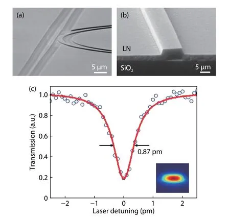
Fig. 5. (Color online) SEM images of the microring resonator. (a) Coupling region of micro-ring. (b) Cross-section of waveguide. (c) Lorentz fitting of the resonance peak at 1572.6 nm, the Q-factor is 1.78 million[23].

Fig. 6. (Color online) Optical spectrum of a frequency comb pumped at 1549.927 nm.
LN is a kind of material with diversified properties such as piezoelectric, acousto-optical, electro-optical, nonlinearoptical, photorefractive, photovoltaic, photo-elastic and pyroelectric effect[29]. It is stable, easy to process, and has a large piezoelectric coupling coefficient, which means wider bandwidth[30], more efficient energy transfer, and lower impedance. LN bulk material has been widely used in filters,transducers, microelectromechanical systems (MEMS)[31]and other devices, and its performance and reliability have been fully verified. In recent years, the emergence of LNOI technology[32], simultaneously demonstrating high optical and mechanical quality factors, large opto-mechanical coupling, good piezoelectric coupling efficiency, provides a new idea for the development of high Q and compact OEMS devices.
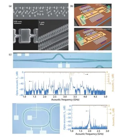
Fig. 7. (Color online) (a) SEM of the one-dimensional optomechanical crystal (OMC) design[33]. (b) Schematic layouts of MZI- and resonator-type AOMs[34]. (c) Microscope image of a suspended acousto-optic MZI and a suspended optical racetrack cavity with a thin-film acoustic resonator and these acoustic S11 and opto-acoustic S21 spectra[35].
Amir H. Safavi-Naeini's Lab at Stanford University make important progress in the optomechanical crystal (OMC) device by demonstrating a photonic crystal resonator on LNOI that simultaneously supports high-Q optical and mechanical modes, where the mechanical modes are coupled piezoelectrically to microwaves. Optical quality factors above 300 000 and mechanical quality factors of 17 000 at cryogenic temperature are measured, leading to opto-mechanical coupling rates g0/2π ≈ 120 kHz by leveraging the photo-elastic effect.This LN OMC platform will open up opportunities for integrated ultra-low-power modulators, quantum microwave-to-optical converters and hybrid systems with densely integrated electrical, mechanical and optical elements[33].
In 2019, Piazza et al.[34]demonstrated the first acousto-optical modulators fabricated on a 500-nm-thick LN thin film sitting on an insulator. This work exhibited the MZI-type acousto-optical modulator and the racetrack-resonator type acousto-optical modulator, as shown in Fig. 7(b). The interdigital transducers (IDTs), acoustic cavity, and low-loss photonic waveguides are fully integrated on chip. In order to maximize the modulation efficiency, the distance between the two arms(DW-W) in the MZI type acousto-optical modulator was set to be at an odd multiple of Λ/2 to enable push-pull operation.The separation DW-Wbetween the two straight waveguide arms of the racetrack-resonator was set to be an even multiple of Λ/2 to maximize the accumulated optical phase change. The effective photo-elastic coefficient was extracted to be 0.053 in the MZI-type AOM, which agrees well with the theoretical value and indicates that the elasto-optic properties are well preserved in the thin film implementation. Much stronger amplitude modulation was achieved in a high Q (>300 000) optical resonator due to the higher optical sensitivity, which exhibits stronger modulation than that of MZI-type AOM and any other integrated platform (e.g., thin film GaAs).
In 2019, Marko et al.[35]demonstrated an integrated acousto-optic platform on thin film LN, which converts acoustic waves in the microwave domain to optical light by a generalized acousto-optic interaction. The author used an interdigital transducer that drives a freestanding 100 μm-long thinfilm acoustic resonator to modulate light traveling in a Mach-Zehnder interferometer or racetrack cavity as shown in Fig. 7(c). The S21spectrum of Mach-Zehnder interferometer features several peaks indicating enhanced microwave-to-optical conversion at acoustic resonances, with the strongest responses measured at the 2.24 and 3.33 GHz acoustic modes,the corresponding Vπ = 4.6 V at the resonance frequency of 3.33 GHz, which means VπL = 0.046 V·cm. The microwave-tooptical conversion efficiency can be further improved by using the acoustic-optic racetrack cavity with Q factor of 2.2 ×10⁶. The author observed a high S21= -7.5 dB at the acoustic resonant frequency of 2 GHz, resulting in a much lower effective Vπ of 0.77 V than MZI, then estimated the acousto-optic single photon coupling strength to be g0~ 1.1 kHz between the 2.17 GHz acoustic mode and the fundamental TE optical mode.

Fig. 8. (Color online) (a) Schematic of poling electrodes and silicon nitride (SiN) strip on 700 nm thick x-cut MgO:LN thin film. (b) Zoomed-in view of poling electrode tip showing 160 nm chromium (Cr) on top of 100 nm SiO2. (c) Poling circuit; pulses generated from an arbitrary waveform generator (AWG) are amplified by a high voltage amplifier (HVA) and applied to a sample covered with silicone oil[37].
5.Second-harmonic generation in PPLN waveguides
PPLN is widely used in second-harmonic generation(SHG)[36], all-optical wavelength conversion, optical parametric amplification (OPA)[8]because of its unique nonlinear effect. Compared with the traditional bulk material PPLN, thin film PPLN has a higher conversion efficiency, because the conversion efficiency of PPLN is inversely proportional to the cross-sectional area, while the cross-sectional area of the thin-film PPLN is much smaller than that of the bulk material PPLN. In addition, thin-film PPLN is easy to process and integrate, and has good process compatibility.
The group from The Ohio State University presented the poling electrodes as Fig. 8(a) shows. Fig. 8(b) provides a zoomed-in view of an electrode with a rounded tip. Fig. 8(c)is a schematic diagram of the polarization circuit. The signal generator generates a voltage pulse waveform, and then amplifies the voltage signal through a high-voltage amplifier. The+z direction of the PPLN adds a positive voltage, and the -z direction adds a negative voltage. Rsis the current limiting resistor, and the oscilloscope is used to monitor the polarization current in the process.
Fig. 9 shows the top-view SEM of a poled MgO-LN waveguide fabricated in our group after etching in hydrofluoric acid. It can be seen that the duty ratio of the inverted domain after polarization is about 1 : 1.
In recent years, many groups have realized efficient second harmonic generation and optical parametric amplification on thin-film PPLN. For example, Harvard University used a nanostructured PPLN waveguide to demonstrate an ultrahigh normalized efficiency of 2600% W-1cm-2for second-harmonic generation[38], as shown in Fig. 10. The highest measured absolute conversion efficiency in their devices is 53%, corresponding to the generation of ~117 mW at 775 nm in the waveguide using a pump power of 220 mW, as shown in Fig. 11. For Nanjing University and Sun Yat-sen University,their periodically poled LNOI waveguide was characterized by SHG at 1470 nm with the normalized conversion efficiency being 3061% W-1cm-2[39]. In addition, DFG was realized with a pumping wavelength at 730 nm in the visible part of the spectrum, and the spectral tuning range of the generated idler in the C-band was 50 nm. The group from University of Central Florida presented thin-film-based ultra-efficient PPLN nonlinear waveguides with 4600% W-1cm-2conversion efficiency for SHG, pumped around 1540 nm[40].
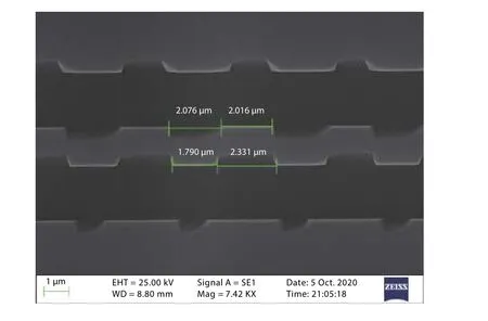
Fig. 9. Top-view SEM of a poled MgO-LN mesa after etching in hydrofluoric acid.
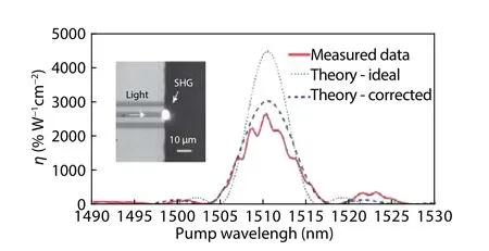
Fig. 10. (Color online) Zoomed-in view of the SHG spectral response of the 1440-nm-wide device (solid curve), together with the theoretically predicted responses[38].
Not only the PPLN waveguide can reach high efficiency SHG, the microring resonators based on PPLN can also achieve higher SHG efficiency than a traditional waveguide.For instance, the group from Yale University demonstrated high-efficiency SHG of 250 000%/W in dual-resonant, periodically poled z-cut LN microrings, where quasi-phase matching is realized by field-assisted domain engineering[41], as shown in Figs. 12 and 13. Otherwise, the group from Stevens Institute of Technology demonstrated quasi-phase-matched frequency conversion in a chip-integrated LN microring resonator, whose normalized efficiency reaches 230 000%/W[42].

Fig. 11. (Color online) SHG total conversion efficiency as a function of input power in the pump-depletion region. The inset shows the inputoutput power relation in the low-conversion limit[38].
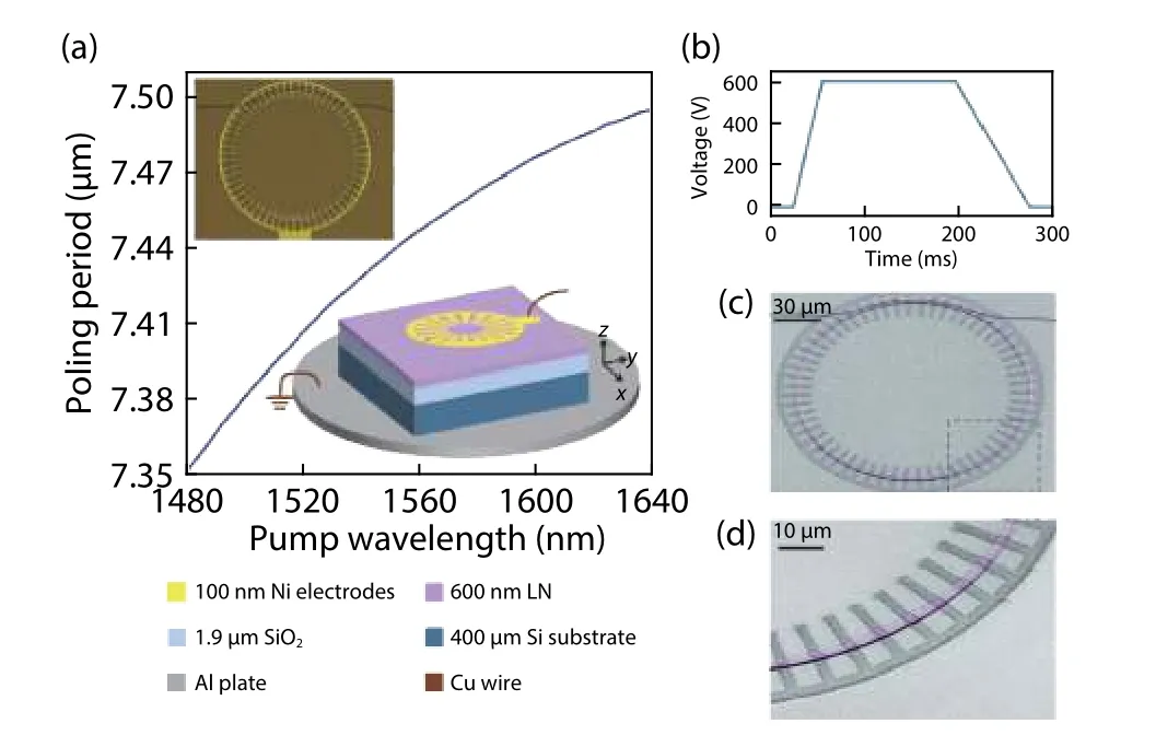
Fig. 12. (Color online) (a) Numerical simulation of the poling period for QPM between the pump TE 00 and SH TM 00 modes using the Sellmeier equation for congruent LN. (b) Applied poling pulse shape. (c, d)False-color SEM images of a PPLN microring resonator etched with hydrofluoric acid and its zoomed-in view, revealing a poling duty cycle of ~35%[41].
In summary, based on the realization of high SHG efficiency of thin-film PPLN, the published work has three extensions. One is to combine with microcavity to increase the frequency doubling slope efficiency by two orders of magnitude to achieve microwatt pumping. The second is to combine with temperature control to achieve tunable center wavelength. The third is to combine with waveguide dispersion engineering to achieve broadband frequency doubling.
At present, our group have produced an MgO-PPLN waveguide with SHG efficiency of 408% and absolute conversion efficiency of 8.32%, but there is still much room for improvement. In the next step, we will try different polarization periods to achieve the best quasi-phase matching.
6.Efficient edge coupling for LNOI
In traditional bulk lithium niobate platform, directly-coupling is widely used. But the huge gap between mode-field-diameter (MFD) of standard-single-mode-fiber (SSMF, ~10 μm)and integrated waveguide on LNOI (< 1 μm) introduces a great coupling loss. The lensed taper fiber is used to reduce the coupling loss, but the experiments does not show a good result[6,38,43]. To realize fiber-chip coupling, various kinds of edge couplers based on LNOI have been reported. For example, chemical-mechanical polishing (CMP) is utilized to fabricate waveguide covered with tantalum oxide[44], but it is hardly compatible with general ridge waveguide. Mode matching between ridge waveguide and tapered and lensed fiber(TLF) through a single ridge taper[45]is also demonstrated,but the coupling loss is still relatively high. To solve these problems, bilayer taper couplers have been proposed to improve the performance[46]. But the mode field distribution of the coupler controlled only by the geometry of the taper’s tip is different with that of fiber. So, it is difficult to further improve the coupling efficiency in that configuration. Recently,researchers reported an edge coupler consisting of a bilayer taper and a cladding waveguide (CLDWG) which was made up of polymer showing a coupling loss of 1.5 dB per facet[47].But the existence of the polymer in the coupler structure can bring mechanical and thermal instability, thereby limiting its application scenarios.
Figs. 14(a) and 14(b) illustrate the schematic structure of the proposed coupler by our group. We fabricated the coupler on a commercially available X-cut LNOI substrate(NANOLN) through standard semiconductor process. The top LN thin film is 500-nm thick. The measured transmission spectrum of the single coupler with HNAF is indicated in Fig. 15(a). At 1550 nm, the coupling loss is 0.54 and 0.59 dB/facet for TE and TM light and the polarization extinction ratio is low than 0.05 dB. The coupler has the coupling loss lower than 1 dB/facet for both TE and TM light at wavelengths longer than 1527 nm. It is expected that the coupler keeps lower than 1 dB/facet in the whole C+L-band (1530 to 1625 nm) according to the curve trend of the transmission spectrum. Comparatively, the coupling loss between edge coupler and SSMF (~10 μm) is 5.7 dB at 1550 nm for TE mode.
Couplers with various tip widths of the lower LN inversed taper were fabricated and tested. The simulated and measured coupling loss at 1550 nm versus different tip widths taper were shown in Fig. 15(b). As expected, the loss rises when the tips get wider, while the loss is still as low as 0.72 dB when the tip width reaches 400 nm. Comparing with the simulation result, the measured additional loss of the coupler might come from the imperfections induced in fabrication process.
7.Conclusion
The recent developments of photonic devices on the LNOI platform were reviewed. A variety of key building blocks for highly integrated photonic integrated circuits(PICs) have been established on this platform. Apart from the extraordinary electro-optical modulation and optical nonlinear generation characteristics, the excellent piezoelectric and acousto-optic properties of LNOI have also been demonstrated in opto-electro-mechanical systems. Furthermore,edge couplers consist of bilayer taper and cladding waveguide have been used to provide efficient fiber-to-chip coupling with loss lower than 1 dB/facet in the whole C+L-band.
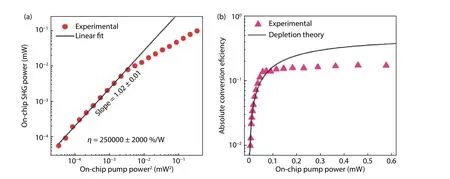
Fig. 13. (Color online) (a) PSHG-Pp2 relation. A linear fit is applied to the experimental data in the low-power region. A fitted slope of 1.02 implies a quadratic dependence of SHG power on the pump power. An SHG conversion efficiency of 250 000%/W is extracted. (b) Absolute conversion efficiency as a function of pump power, including the experimental data and theoretical fit[41].

Fig. 14. (Color online) (a) Structure of the edge coupler. (b) Overhead view of the edge coupler[48].

Fig. 15. (Color online) (a) Transmission spectrum of the fabricated single coupler. (b) Coupling loss versus different tip widths of the lower LN inversed taper (TE mode)[48].
However, a few challenges need to be overcome to make LNOI a commercially attractive and competitive integrated optical platform. (1) Systems on LNOI. Despite the great success in electric-optical and nonlinear devices, LN’s indirect bandgap limits its applications in light sources and photodetectors. Hybrid integration of III-V and Ge optical circuits on LNOI seems to be one of the most promising ways. (2)The limited wafer sizes and high cost per wafer, makes LNOI less competitive as compared with a more mature and cost-efficient wafer platform such as SiN and SOI. Whether LNOI could be widely adopted as a fundamental photonic integration platform is still hard to say. The demonstration of hybrid Si and LN MZI modulator shows another way as integrating local islands of thin film LN onto SOI. (3) Most of the LNOI fabrication techniques are only suitable for prototyping of optical devices in academic laboratories, such as electron-beam lithography and focused ion beam milling, which are incapable of mass production of LNOI-based devices. High performance LNOI optical circuits based on photolithograghy techniques could be expected, with improved photonic designs.
Acknowledgements
This work is supported by the National Key Research and Development Program of China (2019YFB2203800) and the National Natural Science Foundation of China under Grant No.61835008, 61905079, and 61905084. We thank the Center of Micro-Fabrication and Characterization (CMFC) of WNLO and the Center for Nanoscale Characterization & Devices (CNCD),WNLO of HUST for the facility support.
 Journal of Semiconductors2021年4期
- Journal of Semiconductors的其它文章
- Beyond the 100 Gbaud directly modulated laser for short reach applications
- Organic perovskites
- Orthogonally polarized RF optical single sideband generation with integrated ring resonators
- Recent progress in integrated electro-optic frequency comb generation
- Monolithic DWDM source with precise channel spacing
- L atest advances in high-performance light sources and optical amplifiers on silicon
