Recent progress in integrated electro-optic frequency comb generation
Hao Sun, Mostafa Khalil, Zifei Wang, and Lawrence R. Chen
Department of Electrical and Computer Engineering, McGill University, Montreal. QC H3A 0E9, Canada
Abstract: Optical frequency combs have emerged as an important tool enabling diverse applications from test-and-measurement, including spectroscopy, metrology, precision distance measurement, sensing, as well as optical and microwave waveform synthesis, signal processing, and communications. Several techniques exist to generate optical frequency combs, such as mode-locked lasers, Kerr micro-resonators, and electro-optic modulation. Important characteristics of optical frequency combs include the number of comb lines, their spacing, spectral shape and/or flatness, and intensity noise. While mode-locked lasers and Kerr micro-resonators can be used to obtain a large number of comb lines compared to electro-optic modulation, the latter provides increased flexibility in tuning the comb spacing. For some applications in optical communications and microwave photonics, a high degree of integration may be more desirable over a very large number of comb lines. In this paper, we review recent progress on integrated electro-optic frequency comb generators, including those based on indium phosphide, lithium niobate, and silicon photonics.
Key words: electro-optic frequency comb generation; integrated photonics; silicon photonics; integrated lithium niobate; indium phosphide
1.Introduction
An optical frequency comb (OFC), defined as a series of equally spaced and phase correlated discrete optical spectral lines[1], was first reported in the 1960’s with the study of mode-locked lasers (MLLs)[2]. An OFC can be used as an optical frequency ruler for precision spectroscopy and was recognized with half of the 2005 Nobel Prize in Physics awarded to Hänsch and Hall[3,4]. Over the years, the generation of OFCs has been studied intensively and their use in diverse applications have been reported, including optical frequency metrology[5], spectroscopy[6,7], precision distance measurement (Li-DAR)[8], astronomical spectrograph calibration[9,10], optical synthesis[11], RF and microwave photonic (MWP) signal processing[12-14], and optical communications[15-17], amongst others. For example, in optical communications, OFCs can be used to generate sinc-shaped Nyquist pulses which, in turn,can be applied to Nyquist OTDM transmission. Here, the number of comb lines and comb spacing determine the duration of the sinc-shaped Nyquist pulses (more comb lines results in shorter pulses) and the repetition rate of the pulse train, respectively; the spectral flatness of the comb and mutual coherence of the comb lines determine the quality of the pulses in terms of how close they resemble the ideal sinc shape as well as the stability of the pulse train, e.g., in terms of root-meansquare (rms) timing jitter. In MWP signal processing, OFCs can be used to implement tap delay line structures for MWP filtering or for RF channelization. A large number of comb lines will enable a larger number of taps to provide increased flexibility in controlling the MWP filter response or for very broadband RF channelization. Here, an OFC with high spectral flatness is not necessary as programmable optical filters are typically used to control the amplitudes of each tap (comb line) to obtain a specific MWP filter response. Each application has its own requirements or specification on the OFC characteristics,such as the number of comb lines, spectral bandwidth, frequency or comb spacing (or free spectral range, FSR), comb power, spectral flatness, center frequency, and coherence.
These requirements have motivated different techniques for OFC generation. Approaches include MLLs[18,19]assisted by an internal or external reference, micro-resonators with nonlinear optical effects such as four wave mixing driven by parametric oscillation[20-24]or mode locking through the formation of dissipative Kerr solitons[25,26], chaos assisted combs in deformed microcavities[27], and electro-optic (EO) modulation[14,17,28-36]. MLLs can generate broad bandwidth combs,but continuous tuning of the comb spacing is very limited and specially designed laser structures are needed[19]. Pumping a micro-resonator with a single frequency laser and exploiting the nonlinear Kerr effect can generate hundreds of comb lines with extremely broad bandwidth; this approach has also been used to obtain broadband combs in the mid-IR, e.g.,from 2.1 to 3.5 μm[24]. However, the formation dynamics can be complex and in order to obtain a comb with stable amplitude and phase, sophisticated control techniques are required. Moreover, for OFC generation with Kerr or chaos assisted combs, obtaining a flat spectrum as well as tunability of the comb spacing and/or the number of comb lines remains challenging[15].

Fig. 1. (Color online) (a) Generic setup for OFC generation. (b) Schematic of a DD-MZM.
On the other hand, EO modulation provides flexibility in tuning the comb features, such as comb spacing, the number of comb lines, spectral flatness, etc., which can be very desirable for applications in optical communications and MWP.Here, a continuous wave signal is modulated by one or more EO modulators driven by one or more RF signal generators to create multiple sidebands. The comb spacing can be tuned by controlling the frequency (or frequencies) of the RF signal(s) while the number of comb lines can be adjusted through the number of modulators used and the corresponding driving conditions. By the appropriate selection of the modulators and careful control of the RF signals and bias voltages, a flat spectrum with high optical signal noise ratio can be obtained. Moreover, there is a growing interest for large-scale integration due to features such as efficiency, compactness, and robustness. Thanks to the advances in the development of high performance integrated EO modulators, onchip generation of OFCs has been demonstrated in different platforms including thin film lithium niobite on insulator(LNOI)[20,37-41], InP[42-45], silicon organic hybrid[33], and siliconon-insulator (SOI)[17,34,46-53]. Various approaches have been considered, such as a single phase modulator (PM)[46], a single microring modulator (MRM)[47], a single dual drive Mach-Zehnder modulator (DD-MZM)[17], IQ or dual parallel MZMs[29]and cascaded modulators, e.g., cascaded MRMs[48-50], cascaded MZMs[51,53], and a combination of both phase and intensity modulators (IMs)[44,52].
In this paper, we review recent developments of integrated EO OFC generation. The purpose is not to provide a comprehensive review of the theory and different approaches,but rather to highlight some key results that have been obtained and with a specific focus on those achieved in the SOI platform. The remainder of this paper is structured as follows.We describe some basic theory of EO OFC generation in Section 2, followed by a review of the state-of-art integrated technologies in Section 3. Specifically, we describe results obtained using InP, LNOI, and SOI, including single and cascaded MRMs, single DD-MZMs, and cascaded modulators. Finally, we compare the different integrated approaches in Section 4 and conclude.
2.Electro-optic comb generation
Three main components are used for EO OFC generation:a continuous wave (CW) laser, one or more EO modulators,and RF signal generator(s), see Fig. 1(a). The output spectrum is centered at the wavelength of the CW laser and for a single EO modulator, the comb spacing is determined by the RF signal generator. Cascading two or more EO modulators leads to a greater number of comb lines and correspondingly, a larger bandwidth. The number of comb lines is dependent on the modulation depth obtained in each modulator,


Fig. 2. (Color online) (a) Schematic of an intracavity MRM. (b) Transmission spectrum of an MRM (the input laser wavelength is shown in red for illustration).
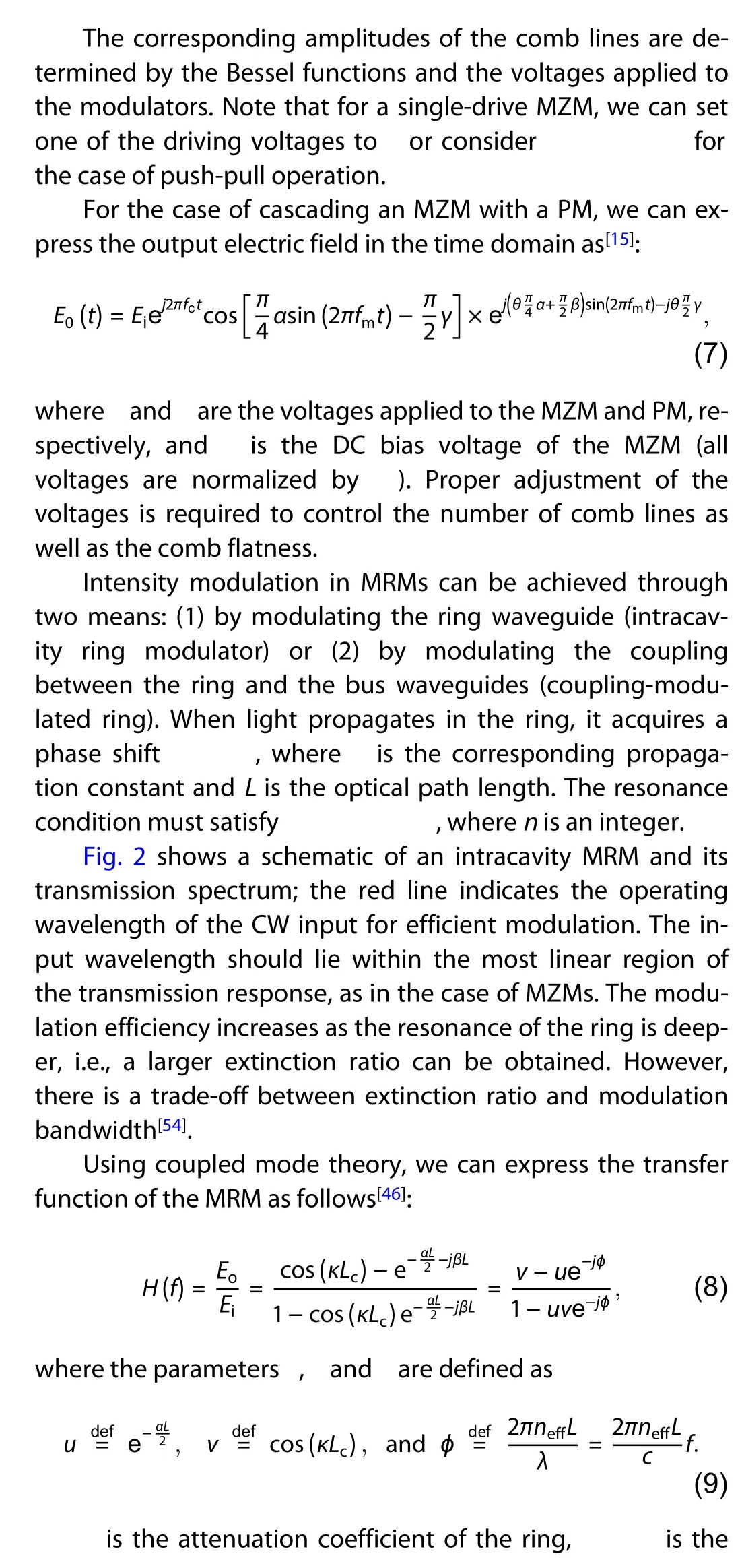
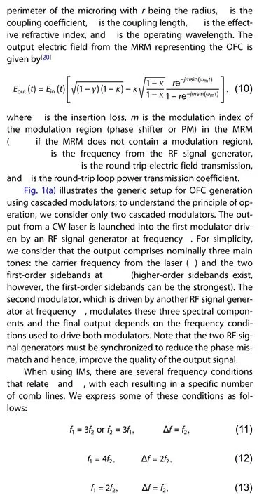

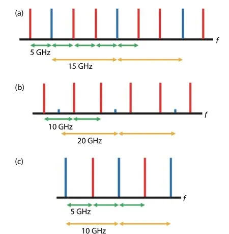
Fig. 3. (Color online) OFC generation using different driving conditions: (a) f 1 =3f2 , (b) f 1 =4f2 , and (c) f 1 =2f2. The blue and red lines depict the output from the first and second modulator, respectively.
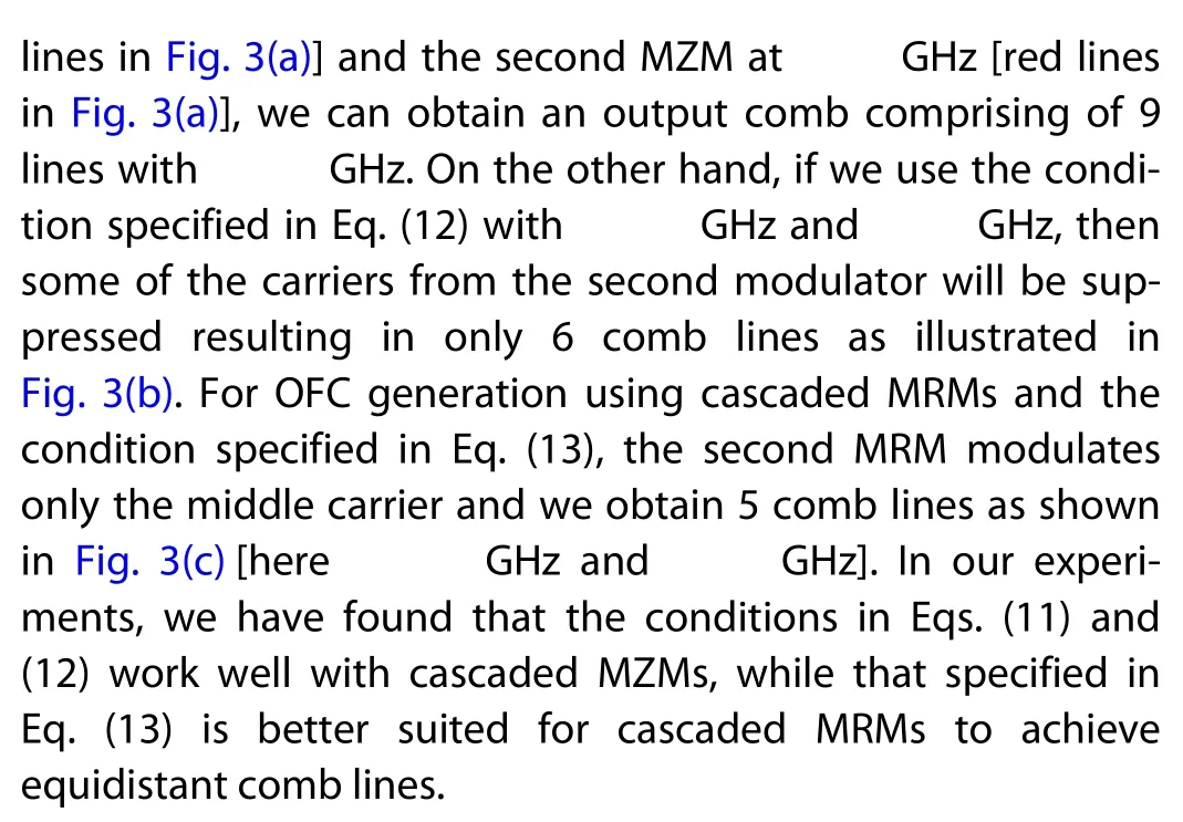
It is also possible to generate OFCs using a cascade of PMs and IMs, e.g., 3 PMs and an IM, or cascading a DD-MZM and a PM. Of course, cascading three or more optical modulators leads to a more complex system which requires greater control over tuning the phase shifters between the modulators and proper adjustment of the driving RF power[15,28].
3.Integrated electro-optic comb generation
3.1.OFC generation in InP
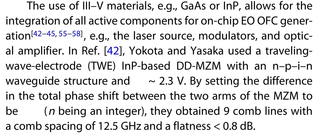
In Ref. [43], Slavík et al. realized a more compact OFC generator that comprised an integrated C-band tunable laser with a dual-electrode MZM in a single package. The output optical power of the tunable laser was 13 dBm while the total loss of the push-pull modulator was ~ 6 dB (including
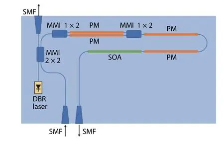
Fig. 4. (Color online) Schematic of the InP-based OFC generator in Refs. [44, 45]. SMF: single mode fiber; MMI: multimode interferometer;DBR: distributed Bragg reflector; PM: phase modulator; SOA: semiconductor optical amplifier.
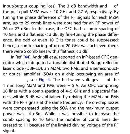
To increase the number of comb lines, Bontempi et al. exploited a dual-drive configuration[45]for the MZM using the same integrated circuit design shown in Ref. [44]. Here, one arm of the MZM was driven with an RF signal at frequency f,while the other arm and the PMs were driven by a synchronous RF signal at frequency 3f. They achieved an OFC with 44 comb lines, a comb spacing of 1 GHz, and a spectral flatness of 3 dB. By injecting multiple CW laser lines, they were able to wavelength multiplex multiple OFCs to increase the overall operating bandwidth. In particular, using an external multi-wavelength source, they generated and combined two OFCs centered at 1552 nm (~17 comb lines with ~3 dB flatness) and 1553 nm (~11 comb lines with ~3 dB flatness).
3.2.OFC generation in LiNbO3
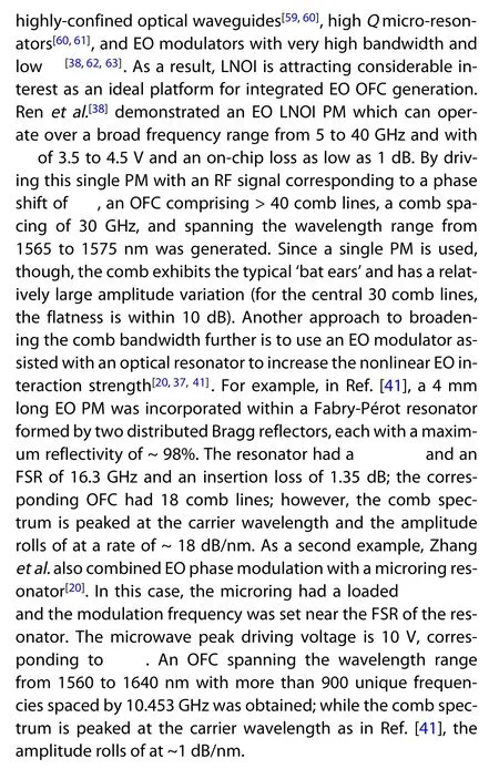
Lithium niobate is an excellent photonic material due to its advantages of large second order nonlinearity and ultrabroad transparent window from 350 to 5000 nm[59]. Recently, the rapid development of micro and nano fabrication techniques has allowed for the realization of high quality integrated optical devices based on LNOI, including low-loss and

Fig. 5. (Color online) Typical experimental setup for OFC generation using (a) single MRM, (b) cascaded MRMs.
3.3.OFC generation in SOI
3.3.1. Microring modulators
Two setups commonly employed for OFC generation with MRMs are shown in Fig. 5. In Fig. 5(a), the output from two RF signal generators, one at f and the other at 2f, is used to drive a single MRM (the phase difference between the two RF signal generators is tuned using a phase shifter).In Fig. 5(b), two cascaded MRMs are used, each driven by a separate RF signal generator. In both cases, the OFC spectrum depends on the operating conditions as described in Section 2.
In Ref. [34], a CMOS compatible process was used to fabricate an intracavity MRM. The microring had a radius of 14 μm and a coupling gap of 240 nm to the bus waveguide (for operation near the critical coupling point). The bus and ring waveguides had a width of 450 nm, a height of 220 nm, and a slab height of 90 nm. The waveguides were loaded with a PN junction implanted with phosphorus and boron to form N and P regions, respectively. For this design, a π phase shift could be obtained at critical coupling, which was achieved at a forward bias voltage of 1 V. An OFC with 5 comb lines, a comb spacing up to 10 GHz, and a flatness within 0.7 dB was obtained using a setup similar to that shown in Fig. 5(a).
In Ref. [47], an OFC comprising 12 comb lines with a comb spacing of 10 GHz was achieved using an MRM followed by a microring filter. The device was fabricated on a 220 nm SOI platform. A lateral PN junction was loaded on the circumference of the ring to deplete the free carriers. At zero bias voltage, the device had an extinction ratio of 20 dB (confirming operation near the critical coupling point). In reverse bias, the resonance exhibited a red-shift of ~ 27.5 pm/V. Both the MRM and microring filter were identical and designed with a radius of 7.5 μm and a coupling gap of 200 nm. The 3 dB bandwidth of the MRM was around 18 GHz. The microring filter was used to equalize the 5 middle lines.
In Ref. [48], Xu et al. proposed using cascaded MRMs for OFC generation using the frequency condition specified in Eq. (13). Both intracavity MRMs were identical, with a radius of 10 μm and a coupling gap of 315 nm. The lateral PN junctions covered 70% of the circumference, and the metal heater covered 95% of the circumference. The waveguides that form the microrings had a width of 500 nm, a height of 220 nm, and a slab height of 90 nm. When no bias voltage was applied, one MRM had an extinction ratio of 26 dB. The 3 dB bandwidth was measured to be about 25 GHz. Using a setup similar to that shown in Fig. 5(b) with RF signal generators at 20 and 10 GHz driving the first and second MRMs, respectively, they obtained an OFC with 5 comb lines, a comb spacing of 10 GHz, and a flatness within 8 dB.
We also investigated the use of cascaded MRMs for EO OFC generation[49,50]. In contrast with Ref. [48], our MRMs are based on a microring coupled to a 2 ×16 μm2multimode interference (MMI) coupler; the waveguide that shapes the ring is loaded with a PN junction while the MMI coupler is loaded with a PIN junction. The MMI is added to increase the fabrication tolerance and to make the modulator less sensitive to polarization variations[64]. Phosphorus and Boron were used to create the N and and P regions, respectively. The bus and microring waveguides were 500 nm in width, 220 nm in height,and 90 nm in slab height. Two 14 μm linear tapers were added between the MMI section and the input-output waveguides to reduce the mode mismatch loss. Fig. 6 shows the schematic diagram of the MRM, the cross-section of the PN junction loaded on the microring, and a microscopic image of one MRM. A voltage of 1.6 V was required to obtain a π phase shift for each 1 cm of the rib waveguide.
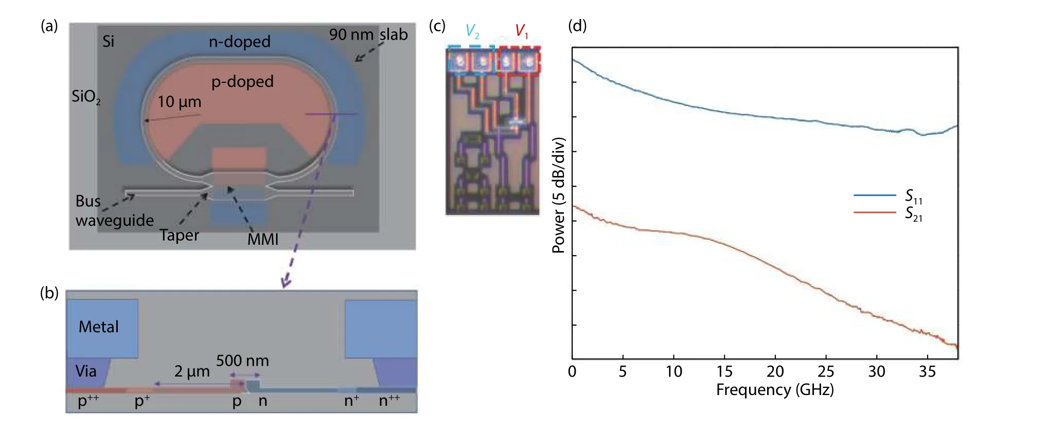
Fig. 6. (Color online) (a) Schematic of the proposed MRM. (b) Cross-section of the PN junction of the ring. (c) Microscopic image of one MRM.(d) S11 and S21 measurements of one MRM.
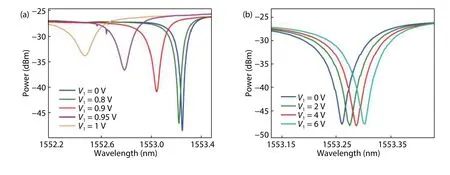
Fig. 7. (Color online) Transmission spectrum of one MRM in (a) forward bias and (b) reverse bias.
For OFC generation, we only focused on driving the PN junction (microring waveguide) with no voltage applied to the MMI. We start by identifying the DC characteristics of one MRM by applying forward bias and reverse bias in the PN junction as shown in Figs. 7(a) and 7(b), respectively. When there is no voltage applied to the microring, the device exhibits a deep resonance at around 1553.3 nm. Under forward bias,there is a blue-shift in the resonant wavelength since free carriers are injected into the PN junction causing a reduction in the refractive index. The opposite phenomenon occurs under reverse bias (red-shift). Fig. 6(d) shows the measured S11and S21responses of a single MRM; the 3 dB bandwidth normalized to the value at 1.5 GHz is ~ 5 GHz.

From the previous reported cases, the output frequency comb spectrum is limited by the 3 dB bandwidth of the MRM used. The comb amplitude variations are limited by the resonance steep (extinction ratio), namely, if the MRM operates in its critical coupling, the intensity at the resonance wavelength exhibit an abrupt π phase shift indicating a better modulation efficiency than over-coupling or under-coupling conditions. The number of comb lines depends on the frequency conditions used to drive the RF signal generators as discussed before.
3.3.2. Dual-drive MZMs
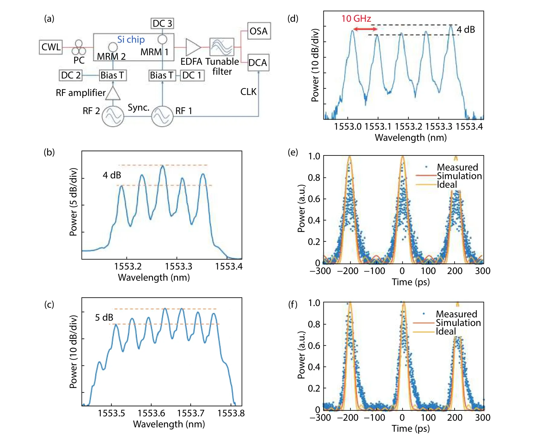
Fig. 8. (Color online) (a) Experimental setup. (b) Driving MRM 1 with 10 GHz and MRM 2 with 5 GHz. (c) Driving MRM 1 with 5 GHz and MRM 2 with 15 GHz. (d) Comb spectrum demonstrating 5 lines when driving MRM 1 at 20 GHz and MRM 2 at 10 GHz. (e) Temporal waveform of (b).(f) Temporal waveform of (c).
Recently Lin et al. explored the use of a single DD-MZM in SOI for EO OFC generation[17]. The modulator was based on depletion-mode PN junctions as phase shifters for high speed operation as well as heaters in the interferometer arms for fine-tuning the phase. Rib waveguides were used with a width of 500 nm, a height of 220 nm, and a slab height of 90 nm. The length of the phase shifters was 4.5 mm, and the half-wave voltage Vπis ~ 6 V. The modulator had a 3 dB bandwidth of 16.8 GHz at a reverse bias voltage of -3.5 V. For OFC generation, two RF signal generators at 20 and 40 GHz frequency were used to drive the upper and lower arms of the DD-MZM, respectively. 5 comb lines with a comb spacing of 20 GHz were obtained with spectral flatness within 9 dB, and a tone-to-noise ratio of 40 dB after amplification. To demonstrate the quality of the comb lines, each was used for Nyquist-WDM transmission and a bit rate up to 800 Gb/s was achieved with 16 Gbaud 32 QAM modulation; each channel had a BER below 2 × 10⁻².
3.3.3. Cascaded MZMs
Fig. 9 shows the principle of OFC generation using cascaded MZMs, which is a generalization of Fig. 3 and the operating conditions specified in Eq. (11). As the DC bias of each MZM has an impact on the power level of each comb line,we can shape the spectral profile of the OFC by tuning the DC bias for each MZM. One important application of this schematic is to generate sinc-shaped Nyquist pulses, or correspondingly, an OFC with a rectangular spectral profile. Note that while it is possible to generate OFCs by cascading several PMs, especially to increase the number of comb lines, this comes at the expense of degraded sideband suppression[52,53].
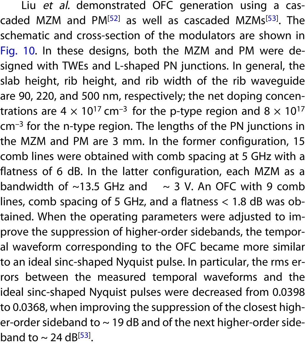
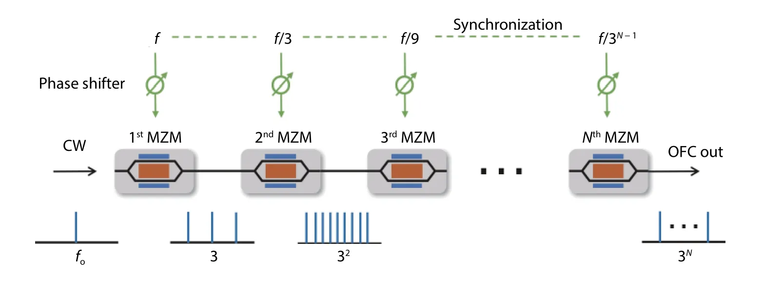
Fig. 9. (Color online) Schematic of cascaded MZMs for OFC generation.
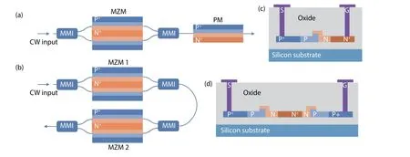
Fig. 10. (Color online) Schematic of integrated cascaded MZM and PM (after Ref. [48]) and cascaded MZMs for EO OFC (after Ref. [53]).
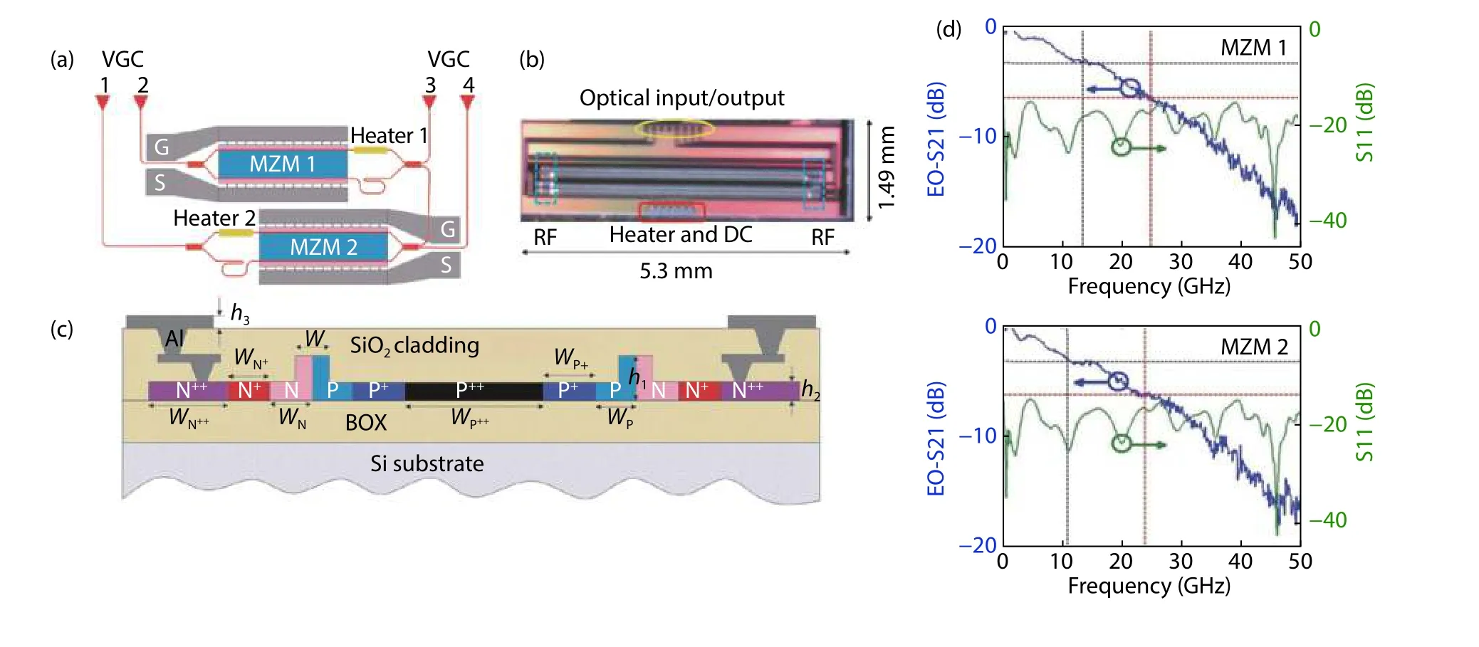
Fig. 11. (Color online) Schematic of the OFC generator in silicon photonics.

Table 1. Parameters of the TW-MZM[51].
We have also demonstrated OFC and Nyquist pulse generation using two cascaded MZMs[51]. Our configuration comprises two cascaded travelling wave MZMs (TW-MZMs) with 3 dB bandwidths ~ 12 GHz, as shown in Fig. 11. Four vertical grating couplers (VGCs) were designed for optical in/out. In particular, VGC 1 (output) and VGC 2 (input) were used for OFC generation while VGC 3 and VGC 4 were designed for characterization of MZM 1 and MZM 2 by coupling CW light into VGC 2 and VGC 1, respectively. For the TW-MZMs, the rib waveguide has the same configuration with the design in Refs. [48, 49], while the lateral PN junctions are used for the phase shifts. The TW-MZM design and parameters are shown in Fig. 11(c) are specified in Table 1. The TW-MZM uses a push-pull configuration and has a path imbalance of 130 μm and a length ~ 4.55 mm (the net PN junction length is 4.2 mm). An n++doped heater is located at the upper arm for tuningthephase. Thehalf-wave voltagesVπofbothMZMs are 10V and theπ phaseshiftcan also beobtainedataheating voltage of 2.5 V.
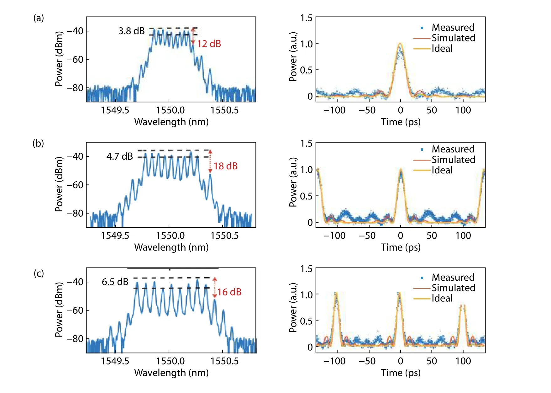
Fig. 12. (Color online) Experimental results of the OFC in silicon photonics. (a-c) the OFCs with spacing from 5, 7.5, and 10 GHz; left: spectral profile; right: temporal signals.
For OFC generation, the CW light was injected into VGC 2 and a quasi-flat OFC can be obtained from VGC 1 by manipulating the heating voltages and reverse DC bias. Compared with the previous results in Ref. [53], we extended the comb spacing to 10 GHz (for an overall bandwidth up 90 GHz) with improved spectral flatness (see Fig. 12). In our experiments,we obtained comb spacings of 5, 7.5, and 10 GHz; the corresponding spectral flatness is 3.8, 4.7, and 6.5 dB, see Fig. 12.The flatness of the quasi-rectangular OFC degrades when the comb spacing is increased; higher RF power and the heater voltages need to be further optimized to improve the flatness. The corresponding temporal waveforms are shown in Fig. 12 and are in great agreement with ideal sinc-shaped Nyquist pulses (assuming a perfect rectangular OFC shape).The full width half maximums for the waveforms in Figs. 10(a), 10(b), and 10(c) are 17.6, 13.1, and 11.4 ps; the corresponding rms timing jitters are 1.2, 1.7, and 1.1 ps, respectively, showing the high quality of the generated pulses.
4.Outlook
Integrated technologies for EO OFC generation have been attracting growing attention in recent years. A summary of results obtained using InP, LNOI, and SOI is given in Table 2.
One of the greatest advantages of using InP is the integration of optical sources with modulators, as well as optical amplifiers to increase the output power. Although only modest output powers (e.g., -4 dBm) have been reported to date, higher values should be possible, e.g., using booster SOA designs.Moreover, wavelength multiplexing of locked integrated multi-wavelength sources is possible thereby allowing for the generation of broadband combs for various applications such as Nyquist WDM transmission[16].
With SOI, while the number of comb lines demonstrated to date has been modest, the spectral flatness has been reasonable, corresponding to the generation of Nyquist pulses of high quality. Moreover, the comb spacing achieved is comparable to commercial LiNbO3waveguide modulators. Silicon photonic modulators with bandwidths up to 45 GHz have been demonstrated[65]; however, careful circuit design is essential to limit parasitics that can otherwise reduce bandwidth in cascaded configurations. One of the main advantages of SOI is that a wide range of high performance passive devices,such as optical filters and dispersive delay lines, are readily available, allowing for the design of integrated subsystems capable of realizing complex functions with high performance.For example, combining cascaded modulators that allow for tunable OFC generation with programmable multi-functional integrated nanophotonics[66]opens the door for numerous optical and MWP signal processing applications. On the other hand, the fiber-to-fiber loss will still need to be addressed.While improved VGC designs can reduce coupling loss, the lack of on-chip amplification compared to InP can limit the amount of processing that can be performed, e.g., even when using high performance programmable devices as the typical silicon nanowire waveguide propagation loss is on the order of 1.5 to 3 dB/cm. In this context, hybrid integration with InP should be considered or may be required.
Perhaps the most exciting development has been the realization of efficient EO phase shifters and modulators in LNOI.PMs with resonators can certainly achieve a very large num-ber of comb lines albeit with a sloped amplitude response(i.e., limited spectral flatness). They have low insertion loss and are compact. It should also be possible to realize cascaded modulators thereby allowing for the generation of broadband OFCs with reasonable spectral flatness. Such OFCs can be used for Nyquist OTDM or Nyquist WDM transmission.They can also be combined with various passive devices, including microring resonators or Bragg grating devices[67,68]to realize integrated MWP subsystems as well as programmable multi-functional integrated nanophotonics on LNOI.
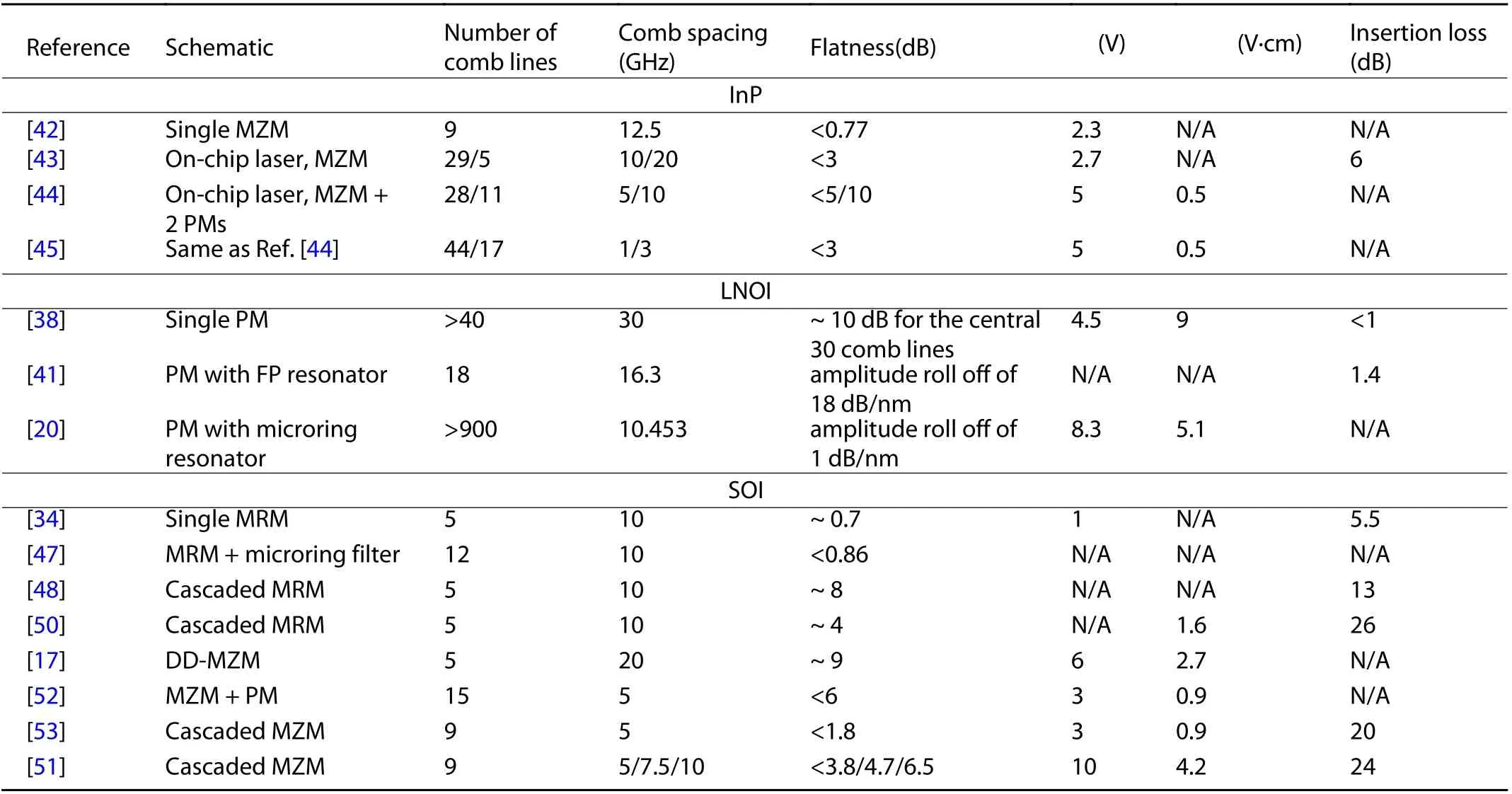
Table 2. Summary of integrated EO OFC generation results.
Acknowledgements
This research was supported in part by the Natural Sciences and Engineering Research Council of Canada and the Fonds du Québec - Nature et Technologies. We thank M. Ma,R. Adams, K. Yim, X. Jin, R. Maram, B. Naghdi, A. Sarmani, M.Jacques, and D. V. Plant for their contributions.
 Journal of Semiconductors2021年4期
- Journal of Semiconductors的其它文章
- Beyond the 100 Gbaud directly modulated laser for short reach applications
- Organic perovskites
- Orthogonally polarized RF optical single sideband generation with integrated ring resonators
- P hotonic devices based on thin-film lithium niobate on insulator
- Monolithic DWDM source with precise channel spacing
- L atest advances in high-performance light sources and optical amplifiers on silicon
