Monolithic DWDM source with precise channel spacing
Lianping Hou, Song Tang, and John H. Marsh
James Watt School of Engineering, University of Glasgow, Glasgow, G12 8QQ, UK
Abstract: We report a low-cost manufacturing approach for fabricating monolithic multi-wavelength sources for dense wavelength division multiplexing (DWDM) systems that offers high yield and eliminates crystal regrowth and selective area epitaxy steps that are essential in traditional fabrication methods. The source integrates an array of distributed feedback (DFB)lasers with a passive coupler and semiconductor optical amplifier (SOA). Ridge waveguide lasers with sampled Bragg side wall gratings have been integrated using quantum well intermixing to achieve a fully functional four-channel DWDM source with 0.8 nm wavelength spacing and residual errors < 0.13 nm. The output power from the SOA is > 10 mW per channel making the source suitable for use in passive optical networks (PONs). We have also investigated using multisection phase-shifted sampled gratings to both increase the effective grating coupling coefficient and precisely control the channel lasing wavelength spacing. An 8-channel DFB laser array with 100 GHz channel spacing was demonstrated using a sampled grating with two πphase-shifted sections in each sampling period. The entire array was fabricated by only a single step of electron beam lithography.
Key words: lasers; distributed-feedback; diode laser arrays; multiple quantum well (MQW) modulators; semiconductor optical amplifier; integrated optics devices
1.Introduction
New approaches are needed for manufacturing optoelectronic hardware, particularly in the access network where increasing data rates need to be provided at low cost. For example, standards for the next generation of passive optical networks (PONs) envisage dense wavelength division multiplexing (DWDM) supporting aggregate data rates of 40 Gb/s[1]and beyond, and requiring optical launch powers > 10 dBm.Monolithic arrays of lasers are considered to be the most promising approach to deploy in these DWDM systems because of their high energy efficiency, small form factor, and high reliability[2]. A multi-wavelength distributed feedback (DFB) laser array requires no dynamic wavelength tuning so can be switched rapidly between WDM channels with each laser operating in a single, stable longitudinal mode (SLM)[3]. However,in such applications the wavelengths must be aligned with the International Telecommunication Union (ITU) grid in which adjacent channels are separated by 100 GHz (0.8 nm).This is done by fabricating an array where the laser wavelengths are spaced by 100 GHz and then using fine temperature and current tuning to align the whole array with the DWDM grid.


We have used ridge waveguides with conventional sampled Bragg gratings (C-SBG) etched into the side-walls[10].All lasers use the same grating period, and the operating wavelengths of individual lasers are set by the sampling period. A modified equivalent phase shift (EPS) of a quarter wavelength was placed at the center of each DFB cavity, a method which significantly increases the SLM yield[5,6]. QWI was used to increase the bandgap of the passive waveguide sections post-growth and reduce the propagation loss. In this way, monolithically integrated DWDM sources operating at 1.55 μm with a wavelength spacing of 0.8 nm were fabricated. The chip comprises four channels (CH) of AlGaInAs/InP DFB lasers, an EAM for each laser, a passive waveguide 4 × 1 multimode-interference (MMI) coupler, and a semiconductor optical amplifier (SOA) output stage. However, the effective grating coupling coefficient κ is greatly reduced when using C-SBGs because part of the sampled period has no grating,and so we will show multi-section phase shifted sampled Bragg gratings (PS-SBGs) can be used to increase the effective κ value.
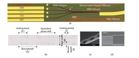
Fig. 1. (Color online) (a) DWDM source optical micrograph. (b) Illustration and relevant dimensions of the side-wall sampled grating with equivalent phase shift. (c) SEM picture of the side-wall sampled gratings. (d) Input part of the MMI coupler.

Fig. 2. (Color online) The simulated C-SBG power reflectivity of the four channels.
2.Device structure and fabrication
The structure of the epitaxial layers[11]and the fabrication processes[12]have been reported previously.
Fig. 1(a) shows an optical microscope picture of a single chip, together with its dimensions. The pitch between adjacent lasers was 125 μm and their ridge width was 2.5 μm.QWI was used to widen the bandgap in the MMI and S-bends by around 100 nm. The 4 × 1 MMI coupler was 30 μm-wide and 532 μm-long [Fig. 1(d)]. The raised cosine S-bends were 1020 μm-long. To minimize facet reflectivity, the SOA was fabricated as a curved waveguide terminating at an angle of 10°to the facet normal. The SOA compensated for the intrinsic loss of 6 dB of the 4 × 1 MMI coupler and allowed the output power to be increased to > 10 dBm. The SOA also can be used to shutter the output when the wavelength is being switched[13]. The four DFB lasers had the same length of 1155 μm. The common grating pitch (Λ) was 232 nm to provide a 0th order Bragg wavelength of 1.480 μm, which was deliberately designed to be far away from the gain peak at ~1.55 μm to avoid lasing in the 0th order mode (see Fig. 2). The CHl to CH4 sampled grating periods Z0were 4.717, 4.764, 4.811, and 4.858 μm respectively, to achieve a wavelength spacing of 0.8 nm (see Fig. 2). Z1was the length of the sample burst, with a 50% duty cycle (Z1= Z0/2). The grating was of first order and was formed by etching recesses of depth d = 0.6 μm into the sidewalls of the waveguide[Fig. 1(c)] in the burst regions. The coupling coefficient of a continuous grating, κ0, was determined using the subthreshold spectral fitting method[14]to be ~80 cm-1. The effective coupling coefficient of a sampled grating is given by κ = 80/π = 25.5 cm-1(see Section 4 below). A λ/4 EPS was located at the center of each DFB laser [Fig. 1(b)]. The EAMs,based on the IEL scheme to simplify the fabrication process,were 150 μm-long and capable of operating data rates at> 5 Gb/s (see Fig. 4(d)).
Simulations of the power reflectivity of the sampled gratings are shown in Fig. 2, in which the waveguide internal loss of 15 cm-1has been taken into account. As noted above, the operating wavelengths of the lasers were determined by the+1st order reflection peaks and lay between 1556.54 and 1554.14 nm with a spacing of 0.8 nm. The -1st order wavelengths lie around 1410 nm where the modal gain is too low to support laser operation.
3.Device performance
The DFB laser threshold currents were ~100 mA corresponding to a current density of 3.46 kA/cm2, which is slightly higher than that of traditional buried grating ridge waveguide DFB lasers (2.29 kA/cm2)[15].
In Fig. 3(a), it can be seen that the DFB laser wavelength can be tuned by changing its drive current, and the tuning rate was determined to be 0.013 nm/mA. When the current is held constant, the tuning coefficient is around 0.1 nm/K over the range -5 to +70 °C. The current tuning range of each DFB laser was around 2.3 nm, and the largest wavelength difference between DFB1 and DFB4 was 4.61 nm. During current tuning, no mode hopping was observed.
With IDFB= 300 mA (3Ith), ISOA= 150 mA, and VEAM= 0 V,the optical spectra measured at 20 °C from the SOA side are shown in Fig. 3(b). The lasing wavelengths of the four DFB lasers were 1558, 1557.27, 1556.62, 1555.64 nm with a wavelength spacing around 0.8 nm, very close to the simulations presented in Fig. 2 other than the measured wavelengths were redshifted due to heating at higher injection currents (300 mA).

Fig. 3. (Color online) Measured from SOA side of the four channels (a) wavelengths vs IDFB when ISOA = 150 mA, and VEAM = 0 V under 20°C, and(b) optical spectra when IDFB = 300 mA, VEAM = 0 V, and ISOA = 150 mA under 20 °C.
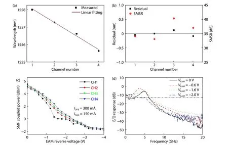
Fig. 4. (Color online) (a) Measured lasing wavelength of the four channels and the curve of its linear fitting. (b) Residual of the lasing wavelength and SMSR of the four channels. (c) Measured ER from coupled SMF of the four channels. (d) Channel 1 small signal E/O response at different VEAM with IDFB = 300 mA, ISOA = 150 mA.
The lasing wavelengths of the four channels from Fig. 3(b) and a linear fit with a gradient of -0.8 nm/CH are shown in Fig. 4(a). The residual error of the four channel lasing wavelengths after linear fitting of the lasing wavelengths versus the channel number is shown in Fig. 4(b). The residuals vary from -0.084 to 0.13 nm; the small magnitudes of the residuals are attributed to the precise control of the sampled grating periods, Z0, and grating pitch, Λ, offered by EBL. The residuals can be eliminated either by slightly varying the temperature (< 1.5 °C) using a separate heater in each channel or by changing the drive current (by tuning the current by < 10 mA out of 300 mA). The measured singlemode suppression ratios (SMSRs) are shown in Fig. 4(b); all SMSRs exceed 33 dB, demonstrating excellent SLM operation of the DWDM source. By comparing the spectra from the SOA and DFB sides, it can be seen there is no degradation associated with the SOA.
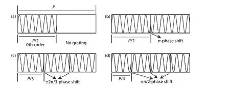
Fig. 5. Schematic structures of (a) C-SBG, (b) 2PS-SBG, (c) 3PS-SBG, and (d) 4PS-SBG. P is the sampling period.
The power coupled into a single mode fiber (SMF) for the four channels when IDFB= 300 mA, ISOA= 150 mA is shown in Fig. 4(c). The true maximum power from the SOA side should be more than 10 mW because the coupling efficiency to the SMF was less than 30%[16]. The residual output power at VEAM= -4 V arises from amplified spontaneous emission in the SOA. Using an arrayed waveguide grating (AWG) combiner in place of the MMI would improve the direct current (DC)extinction ratio (ER) because the loss associated with a 4 × 1 MMI coupler is always > 6 dB. The small signal RF performance of the CH1 EAM is presented in Fig. 4(d) under the operating conditions of IDFB= 300 mA, ISOA= 150 mA. The -3 dB bandwidth was about 6.6 GHz at VEAM= -1.6 V, which means each channel is capable of encoding data at > 5 Gb/s. The anomalous trend of the bandwidth vs VEAMin the E/O response of the EAM and the appearance of a resonance peak around the relaxation oscillation frequency indicate that there is electrical or optical coupling between the EAM and the DFB laser[7]. Electrical coupling could originate from insufficient isolation between the EAM and laser (the measured isolation resistance is about 2 kΩ) and could be reduced substantially using proton implantation[17]. Optical coupling can be attributed to residual reflections from the MMI and/or SOA. The MMI was specifically designed to reduce back-reflections,with a 45° tilt at each corner of the input and output waveguides, reducing the back reflections at the input waveguides of the MMI by at least 10 dB[18]. The major back-reflection therefore arises from the SOA output facet, which could be suppressed with an anti-reflection (AR)-coating on the output facet. Reducing the device and stray capacitance by deep etching the EAM section[19], making the bond pads smaller and using semi-insulating substrates would enable the operating speed to be increased substantially[20].
4.Multisection PS-SBG
As can be seen in Figs. 1(b) and 1(c), every sampled period of a C-SBG structure has a section where the grating is absent, which will reduce the κ value. Because the design uses±1st-order reflections and a 50% sampling duty cycle, the effective κ is reduced to 1/π (~ 0.32) times that of the κ of a uniform grating[21]. The 0th-order reflection still has the highest reflection coefficient [Fig. 6(a)] but is displaced from the gain peak to prevent lasing at this wavelength. Recently we have proposed using multisection PS-SBGs in DFB laser arrays as these can have both high κ and precise channel spacing[22].The grating structure of a C-SBG is shown in Fig. 5(a).Fig. 5(b) shows a design with two phase-shifted sections in a single sampling period (2PS-SBG), in which a π-phase-shifted 0th-order grating fills the half of the sampling period where there would be no grating in the equivalent C-SBG. In a 2PSSBG structure, the 0th-order reflection disappears, and the effective κ of the ±1st-order channels is doubled compared to that of the C-SBG, with a value of 2/π (~0.64) times that of a uniform grating [Fig. 6(b)]. Similarly, the sampling period can be further divided into more sections to achieve progressively higher effective κ values. If one sampling period P is divided into m equal sections (m > 2), so every section has a length P∕m, the phase shift between adjacent sections should be set as ±2π∕m. The grating designs for three phase-shifted sections in a single sampling period (3PS-SBG) and four phase-shifted sections in a single sampling period (4PS-SBG)are shown in Figs. 5(c) and 5(d) respectively. The simulated reflection spectra of a 3PS-SBG and a 4-PS-SBG are shown in Figs. 6(c) and 6(d). Their effective κ values are increased to 0.83 and 0.9 times that of the uniform grating. Here the 0th-order Bragg wavelength is designed to be at 1550 nm.
The characteristics of the reflection spectra of the C-SGB,2PS-SBG, 3PS-SBG, and 4PS-SBG and their effective κ values compared with a uniform grating are summarized in Table 1.
Using a 2PS-SBG scheme with the 0th-order sidewall grating period set at 250 nm and the sampling periods ranging from 7.979 to 9.206 μm, an eight-channel DFB laser array was fabricated with 0.837 nm channel spacing and 0.059 nm residual, as shown in Fig. 7(b)[22]. The SMSR values for all the channels are > 35 dB as shown in Fig. 7(a)[22].
Because multisection PS-SBGs have a higher κ value, it is possible to reduce the length of the DFB cavity with a corresponding reduction in the threshold current. The technique can also be used in future to fabricate directly modulated DFB lasers.
5.Conclusion
In summary, a 4-channel DWDM source suitable for use in PONs has been demonstrated by a combination of the REC, IEL, and QWI techniques. The device has an output power > 10 dBm and a channel spacing of 0.8 nm (100 GHz).The approach has the advantages of providing accurate control over the individual lasing wavelengths, offering a potentially high SLM manufacturing yield and low manufacturing costs. Using a C-SBG structure, the κ value is reduced to 0.32 times that of a uniform grating (assuming a sampling period duty cycle of 50%), but by using multisection PS-SBG designs,the κ value can be increased while maintaining precise control of the channel wavelength spacing of the DFB laser array.Based on a 2PS-SBG design, an 8-channel DFB laser array was fabricated using a single stage of EBL with a 0.837 nm channel spacing and 0.059 nm residual.
Acknowledegments
This work was supported by the U.K. Engineering and Physical Sciences Research Council (EP/R042578/1) and the National Science Foundation of China (61320106013). We would like to acknowledge the staff of the James Watt Nanofabrication Centre at the University of Glasgow for help in fabricating the devices.
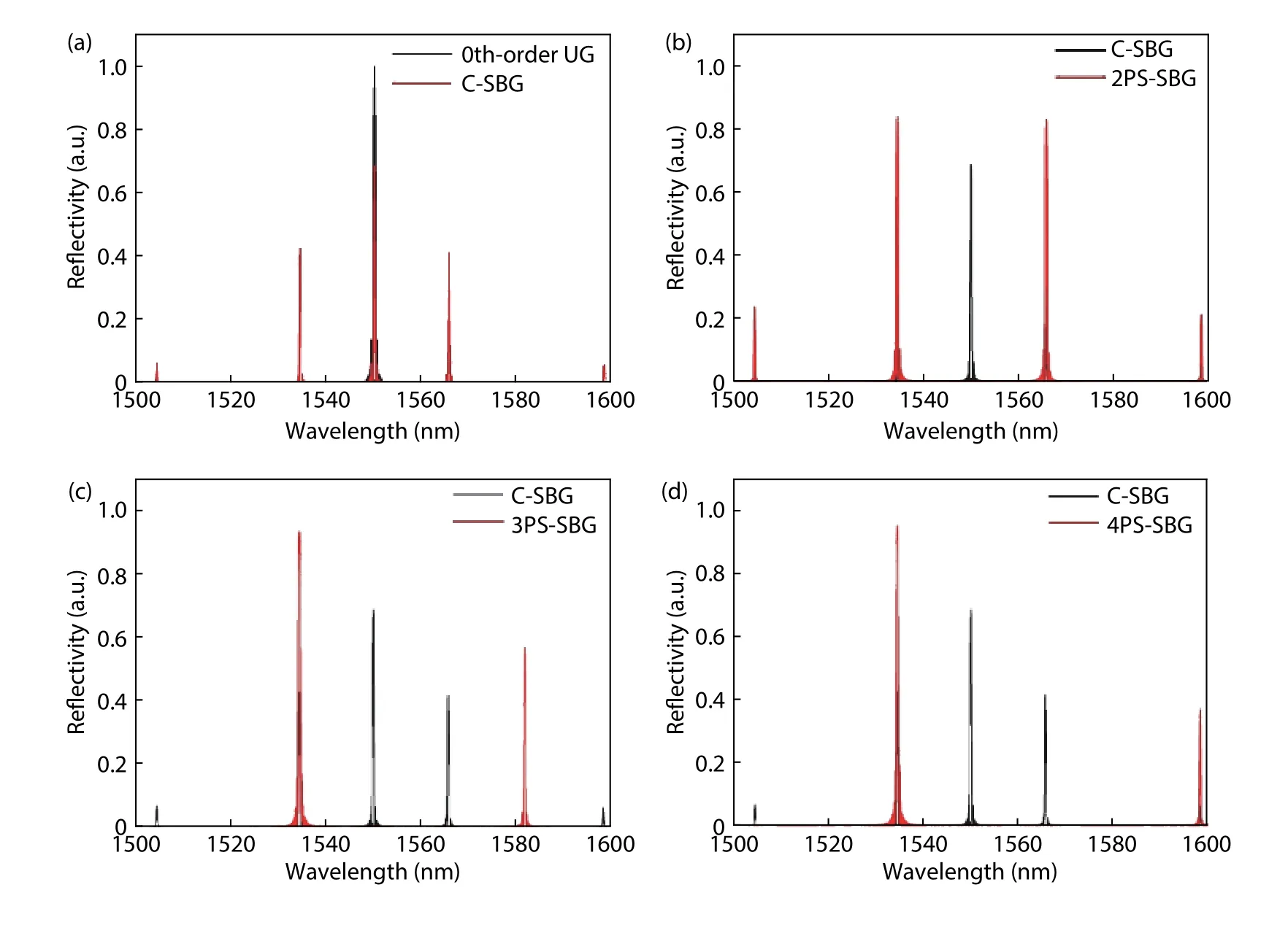
Fig. 6. (Color online) Simulated power reflection comparison between (a) uniform grating (UG) and C-SBG, (b) 2PS-SBG and C-SBG, (c) 3PS-SBG and C-SBG, (d) 4PS-SBG and C-SBG.

Table 1. Comparison between PS-SGB and C-SBG in terms of reflection characteristics and effective κ value.
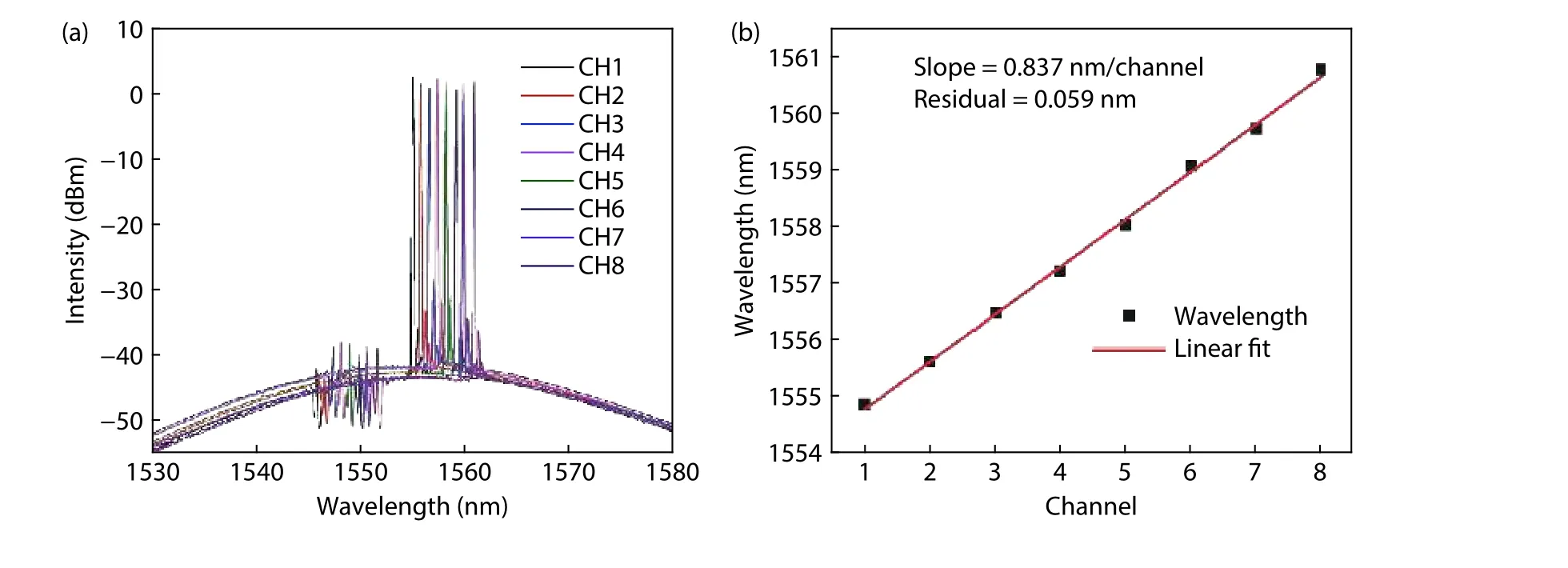
Fig. 7. (Color online) (a) Measured optical spectra of the 8-channel laser array at 100 mA (left to right, channels 1 to 8) and (b) 8-channel lasing wavelengths and the linear fitting.
 Journal of Semiconductors2021年4期
- Journal of Semiconductors的其它文章
- Beyond the 100 Gbaud directly modulated laser for short reach applications
- Organic perovskites
- Orthogonally polarized RF optical single sideband generation with integrated ring resonators
- P hotonic devices based on thin-film lithium niobate on insulator
- Recent progress in integrated electro-optic frequency comb generation
- L atest advances in high-performance light sources and optical amplifiers on silicon
