Exciton emissions of CdS nanowire array fabricated on Cd foil by the solvothermal method*
Yong Li(李勇), Peng-Fei Ji(姬鹏飞), Ya-Juan Hao(郝亚娟), Yue-Li Song(宋月丽),Feng-Qun Zhou(周丰群), and Shu-Qing Yuan(袁书卿)
Key Laboratory of Nano Optoelectronic Materials and Insulation Materials,Pingdingshan University,Pingdingshan 467000,China
Keywords: CdS nanowires array,solvothermal method,photoluminescence,exciton emissions
1. Introduction
For the next generation nanoscale optoelectronic devices,nanostructured semiconductor materials have emerged as potential building blocks.[1]Therefore,nanostructured semiconductors have attracted many researchers’attention.[2,3]Due to the unique physical and chemical properties, the high-quality single-crystalline nanowires have been studied to apply in the nanodevices. For example, silicon nanowires have been applied in the solar cells to enhance the diffusion path of the carriers, which benefits the separation and transition of the photo-generated carriers.[4,5]Consequently, the performance of the device has been improved.
CdS is an important II–VI semiconductor compound,which is characterized by a direct bandgap of 2.4 eV at room temperature, thermal stability, good optical transparency, and electron mobility.[6]It can be used in the fields of optoelectronic devices, such as solar cells, light-emitting diodes, sensors,lasers,and field-effect transistors.[7,8]So,CdS nanowires have been widely studied and applied.[9–15]However, the devices based on CdS nanowires do not show an ideal performance because the surface states and stoichiometric defects in the nanostructured semiconductor generate a large number of carrier trap centers to shorten the diffusion path of carriers and increase the trapped probability of carriers. For better application of CdS nanowires,it is necessary to deeply understand the defects for controlling and tuning them.[16]In the study of white light-emitting diodes,[17,18]some researchers have controlled the chromaticity coordinate and correlated color temperature through tuning the emissions of defects. Photoluminescence spectroscopy,which is a non-destructive and contactless technique,is a powerful tool for investigating the defects in the nanoscale semiconductors.
In the present works, high-quality single-crystal CdS nanowires have been fabricated through solvothermal etching Cd foil in the mixture of the thiosemicarbazide and ethylenediamine, which show (002) growth orientation and are approximately perpendicular to the Cd foil. The room-temperature and temperature-dependent photoluminescence spectra have been measured and analyzed in detail.
2. Experiments
The Cd foil(99.9%)has been used to fabricate CdS in the mixture of the thiosemicarbazide(0.2 mol/L)and ethylenediamine in the teflon-lined stainless steel autoclave. The autoclave is sealed and maintained at 180◦C for 10 h. Afterward,the autoclave is cooled to room temperature, and the Cd foil is taken out from the autoclave, rinsed with deionized water and ethanol several times,and dried in an N2atmosphere. The uniform yellowish precipitate can be observed on the Cd foil.
The morphologies and structures of the CdS nanowires array have been characterized by the field emission scanning electron microscopy (FE-SEM, JSM 6700F), the highresolution TEM(HR-TEM,JEM-2100),and the x-ray diffraction (XRD, Panalytical X’Pert Pro) using Cu Kα radiation source (λ = 1.5406 ˚A). The room temperature and temperature-dependent photoluminescence spectra have been measured and recorded by using a double grating spectrofluorometer(HORIBA,FL3-22)with a closed-cycle helium cryostat (Jannis CCS-100) and a digital temperature controller(LakeShore-325).
3. Results and discussion
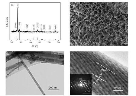
The XRD pattern of the CdS nanowires array is illuminated in Fig. 1(a), which shows a hexagonal structure. From Fig. 1(a), the strongest diffraction peak can be observed and is located at 26.5°, which is indexed to the information of(002) planes of hexagonal CdS (JCPDS: 01-089-2944). It indicates that the CdS nanowire fabricated by the solvothermal method in the present work grows preferentially along the (002) orientation. Figure 1(b) gives the SEM image of the CdS nanowires array. The regular nanowires array can be observed. The CdS nanowires, whose lengths are more than a dozen microns, are approximately perpendicular to the Cd foil. In order to study the fine structure, the yellow materials have been carefully cleaved from the Cd foil and moved into the absolute ethanol. The solution has been vibrated by ultrasound for 5 min and dropped onto the copper mesh. After drying, the studied materials are measured by the TEM system.A single CdS nanowire is uniform and smooth and shown in Fig. 1(c), whose diameter is ~35 nm. The HRTEM image of the individual CdS nanowire is shown in Fig.1(d). The distance of ~0.682 nm can be measured and indexed to the lattice spacing of the planes of 2H-CdS. The nanowire grows along the (002) direction with the closed-packed lattice planes of the hexagonal phase stacked.[19]The inset of Fig.1(d)illuminates the selected area electron diffraction(SAED)pattern of a single CdS nanowire,which suggests that the CdS nanowires are high-quality single crystals nanowires. The SAED pattern shows the corresponding electronic diffraction pattern along the (002) orientation. This is consistent with the analysis of the XRD data.
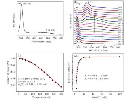
For the nanostructured semiconductor, defects, such as cadmium vacancies, sulphur vacancies, interstitial cadmium,and interstitial sulphur,are inevitable. To apply the nanostructured semiconductor in the optoelectronic device field, it is very important to understand and tune the defects. The photoluminescence is one of the most important research methods,through which the intrinsic recombination processes, radiative and nonradiative recombination processes corresponding to the defects and impurity can be confirmed. In the present works,the room-temperature and temperature-dependent photoluminescence spectra with the excitation wavelength of 450 nm from the xenon lamp have been recorded and shown in Figs.2(a)and 2(b), respectively. From the room-temperature photoluminescence spectrum, two peaks can be observed,which are located at ~505 nm (~2.46 eV) and ~682 nm(~1.82 eV), respectively. The narrow and strong peak can be ascribed to the bandgap emission from the CdS nanowires.The wide and weak peak is originated from the defects of the CdS nanowires.

Fig.1. (a)The XRD pattern,(b)SEM image,(c)low-magnification TEM image,and(d)high-resolution TEM image of CdS nanowires array. Inset: SAED of CdS nanowire.
To investigate the type of defects in detail, the evolution of photoluminescence with the temperature has been analyzed.From Fig. 2(b), four emission peaks can be observed, which change, appear, and disappear with the variation of temperature. To clearly describe the four peaks,we call them P1 peak,P2 peak, P3 peak, and P4 peak from the short wavelength to the long wavelength, respectively. With increasing temperature,the peak positions of the P1 peaks,which are ascribed to the emissions from the bandgap of CdS nanowires, move to the long wavelength. This changing trend of emission position from the bandgap with the temperature can be interpreted as temperature-dependent lattice distortion or exciton-phonon coupling, which can be expressed by using the Varshni equation

where Eg(0) represents the gap energy at 0 K, α is the temperature coefficient, and the value of β is close to the Debye temperature of CdS.The fitting results according to Eq.(1)are shown as the solid line curve in Fig.2(c), which matches the experimental data well. The obtained parameters through the fitting process are α =0.49±0.039 meV/K,β =205±43 K,and Eg=2.54±0.001 eV.The peak intensity of the bandgap emission as a function of the reciprocal temperature is shown in Fig.2(d). There are two obvious different change regions.In the low-temperature range between 10 K and 70 K,the intensity of emission peaks slowly changes. However, in the high-temperature range between 70 K and 300 K, the intensity of emission peaks exponentially changes. It indicates that there are two different recombination mechanisms. The evolution can be expressed as

where I(T) represents the integrated PL intensity at temperature T, I0is the integrated PL intensity at 0 K, A1and A2are the ratios of the nonradiative transition rate to the radiative transition rate, E1and E2are the thermal activation energies.The fitted data well coincide with the experimental data. The values of E1and E2according to Eq. (2) are estimated to be~18.9 meV and ~94.8 meV,respectively.

Fig.2. (a)Room-temperature and(b)temperature-dependent photoluminescence spectra of CdS nanowires array on the Cd foil. (c)The energy of peak as a function of temperature. The solid line is the fitted line according to Eq.(1). (d)Peak intensity of bandgap emission as a function of reciprocal temperature. The solid line is the fitted line according to Eq.(2).
With the increase of temperature,the P2 peaks gradually disappear from ~10 K to ~140 K. However, the energy of the P2 peaks(~564 nm,~2.20 eV)does not show blueshift or redshift. In our previous works,[20]the P2 peaks have been observed and studied in CdS/Si heterojunctions obtained by the chemical bath deposition method, which has shown the variation of the peak position with temperature. In the CdS/Si heterojunctions,the silicon nanoporous pillar array,which has characterization with a regular porous layer consisted of a SiOxmatrix and dispersive silicon nanocrystallites,[21,22]has been used as the p-type materials and substrate. We think that the redshift of the P2 peak in the CdS/Si heterojunctions can be ascribed to the effect of the silicon nanoporous pillar array.So, the mechanism of the P2 peak from nc-CdS in this work is different from that in the previous works. The P2 peak is ascribed to the transition from the holes being bound to the donors or the electrons being bound to the acceptors.[23]The P3 peaks (~623 nm, ~1.99 eV) appear at ~80 K and disappear at ~200 K. Their energies do not vary and are not originated from Icdto Vcd.[24]The P4 peaks can be observed at the temperature range between ~110 K and ~300 K.The transition from Vsto the valence band can contribute to the P4 peaks by combining the result of Fig.2(a).
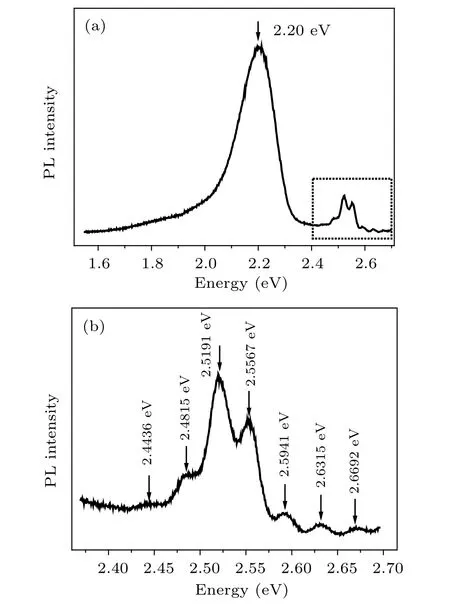
In Fig. 2(b), we observe a broadening of the P1 peak(emission from the bandgap of nc-CdS) at low temperature.As is known, the excitation source obtained from the xenon lamp is characterized by a wider energy range. So,the resulting emission peak might be broadened. In order to minimize the effect of the wide energy of the excitation source,we have reduced the grating slit from 5 nm to 2 nm, and increase the exposure time from 0.1 s to 1.0 s. A photoluminescence spectrum at 10 K has been obtained and shown in Fig. 3(a). The P1 peak appears in the form of multiple peaks. There are two stronger peaks and five weaker peaks. The form of the multiple peaks is separately shown in Fig. 3(b). From low energy to high energy,the peak energies are shown in Table 1. From Table 1,the energy difference(ΔE)between the first peak and second peak can be calculated to be ~39.2 meV.The energy differences of the other adjacent peaks are shown in Table 2.We find that all energy differences are close to 38 meV which is the LO phonon energy in CdS.[13,25]
Due to the spin–orbit coupling and crystal-field, the valence band of CdS has been split into three sub-bands.[23,26–28]The emissions based on three sub-bands have been called EA, EB, and EC, which are characterized with the energies of 2.550 eV, 2,568 eV, and 2.629 eV, respectively.[23,27]Using Eq. (1), Eg(0) is estimated to be ~2.541 eV. Considering the experimental error, in this work, the emission from E4this ascribed to EA, which is originated from the free excitons A.[27,29]The emissions from E6thare ascribed to ECoriginated from the excitons bound to a neutral donor.[27,29]E3rd, E2nd, and E1ston the low energy side of E4thare attributed to the first-order, second-order, and third-order LO phonon replica of E4th, respectively. The first LO phonon replica is more intense than E4th. It indicates that there should exist a strong electron-phonon coupling.[13]E5this the firstorder LO phonon replica of E6th. In the works of Imada and Adachi,[27]E0Cwas estimated to be 2.656 eV. In our work, E7th=2.669 eV. The energy difference between E0Cand E7this ~13 meV. Considering the activation energy E1(~18.9 meV) obtained using Eq. (2), the properties and origin of E7thare similar to those of E0C, which are ascribed to the light polarization parallel to the c axis of hexagonal CdS.

Fig.3. (a)Photoluminescence of CdS nanowire array on the Cd foil at 10 K,(b)the enlarged image of a part of photoluminescence at 10 K.

Table 2. Energy difference of the adjacent peaks.
4. Conclusion
In summary, CdS nanowires array has been fabricated through the solvothermal method, which shows(002)growth orientation and is approximately perpendicular to the Cd foil.Through analyzing the temperature-dependent photoluminescence, four peaks are ascribed to the emissions from the bandgap, the transition from the holes being bound to the donors or the electrons being bound to the acceptors,the transition from Cd interstitials to Cd vacancies, and the transition from S vacancies to the valence band, respectively. At 10 K,the emission originated from the bandgap appears in the form of multiple peaks. From low energy to high energy, the first, second, and third peaks are atributed to the third-order,second-order, and first-order phonon replica of the free exciton A,respectively;the fourth peak is originated from the free exciton A;the fifth peak is atributed to the first-order phonon replica of the excitons bound to neutral donors; the sixth and seventh peaks are originated from the excitons bound to neutral donors and the light polarization parallel to the c axis of hexagonal CdS.
Acknowledgment
The authors are grateful to Professor Xin-Jian Li from Zhengzhou University for his contributions to this work.
- Chinese Physics B的其它文章
- Numerical simulation on ionic wind in circular channels*
- Interaction properties of solitons for a couple of nonlinear evolution equations
- Enhancement of multiatom non-classical correlations and quantum state transfer in atom–cavity–fiber system*
- Protein–protein docking with interface residue restraints*
- Effect of interaction between loop bases and ions on stability of G-quadruplex DNA*
- Retrieval of multiple scattering contrast from x-ray analyzer-based imaging*

