Scanning tunneling microscopic investigation on morphology of magnetic Weyl semimetal YbMnBi2∗
Zhen Zhu(朱朕), Dong Yan(严冬), Xiao-Ang Nie(聂晓昂), Hao-Ke Xu(徐豪科), Xu Yang(杨旭),Dan-Dan Guan(管丹丹),3,4, Shiyong Wang(王世勇),3,4, Yao-Yi Li(李耀义),3,4, Canhua Liu(刘灿华),3,4,Jun-Wei Liu(刘军伟), Hui-Xia Luo(罗惠霞), Hao Zheng(郑浩),3,4,†, and Jin-Feng Jia(贾金锋),3,4,‡
1Key Laboratory of Artificial Structures and Quantum Control(Ministry of Education),Shenyang National Laboratory for Materials Science,School of Physics and Astronomy,Shanghai Jiao Tong University,Shanghai 200240,China
2Department of Physics,National Sun Yat-Sen University,Guangzhou 510275,China
3Collaborative Innovation Center of Advanced Microstructures,Nanjing University,Nanjing 210093,China
4Tsung-Dao Lee Institute,Shanghai Jiao Tong University,Shanghai 200240,China
5Hong Kong University of Science and Technology,Hong Kong,China
Keywords: Weyl semimetal,topological insulator,scanning tunneling microscopy
1. Introduction
In 1929, H. Weyl found that a massless Dirac fermion could be decomposed into one pair of relativistic particles with opposite chiralities,the Weyl fermion. To date,Weyl fermions have not been discovered in high-energy particle physics. Recently, condensed matter physicists discovered that in certain crystals lacking of space inversion or time reversal symmetry,their low-energy quasiparticle excitations could be described by the Weyl equation.[1-45]Hence such a crystal is named as Weyl semimetal. In a Weyl semimetal, lots of novel phenomena, including nonlocal transport and the chiral anomaly effect, have been proposed.[1-4]More interestingly, scientists found that a Weyl cone in the bulk energy bands of a Weyl semimetal carries a non-zero Chern number and therefore the Weyl semimetal is a new generation of topological phase of condensed matter beyond topological insulators. The topology in a Weyl semimetal manifests itself as the exotic disrupted surface band,which terminates at bulk Weyl nodes,the Fermi arc.[1-8]The first Weyl semimetal material was discovered in the TaAs class of crystals.[6-9]Many important predictions including bulk Weyl cones, surface Fermi arc band structure, negative magnetoresistance (chiral anomaly) phenomenon,and novel quasiparticle interference(QPI)were experimentally observed in this class of materials.[1-5]Research on Weyl semimetals has already become a new frontier of condensed matter physics,materials science,and nanotechnology.
According to whether the Lorentz symmetry is conserved,Weyl semimetals can be categorized into two classes. The TaAs class is named as type-I Weyl semimetal, which is Lorentz invariant and obeys the relativistic quantum filed theory. Additionally, a new type (type-II) of Weyl quasiparticle was discovered in WTe2class of materials.[39-43]Type-II Weyl fermions break the Lorentz symmetry, and thus can only emerge as low-energy excitations in a condensed matter system. Therefore, the type-II Weyl fermion is a unique phenomenon of crystal. Another important symmetry is timereversal symmetry. TaAs and WTe2classes of Weyl semimetals are both time-reversal-symmetry invariant. However, a time-reversal-symmetry breaking Weyl semimetal is also predicted to host several novel effects,e.g.,chiral magnetic effect and unconventional superconductivity,which are not possible in the time-reversal-symmetry invariant semimetals.[1-5]Recently, YbMnBi2was discovered as a type-II time-reversalsymmetry breaking Weyl semimetal.[46]It breaks both timereversal and Lorentz symmetries, and thus has become a research focus recently.
Scanning tunneling microscope/spectroscope(STM/STS)is an experimental tool with high spatial, energy, and quasimomentum resolutions. It has been successfully applied to investigate the atomic structure, ionization effect, and quasiparticle interference in many important materials.[47-61]However, for YbMnBi2samples, which are of importance in both fundamental research and potential electronic applications,no STM results have been reported up to date. In this article,we employed STM to study the morphology on the surface of an YbMnBi2single crystal.
2. Results
Our YbMnBi2samples with a size of about 1 mm×1 mm×0.5 mm were grown by the standard flux method. The samples mounted on the sample plate with their(100) surface exposed were cleaved in a ultra-high vacuum system at about 80 K, and then immediately loaded into a commercial STM(Unisoku 1600)for further characterization at 4.8 K. Electrochemically etched tungsten wires were used as the STM tips.

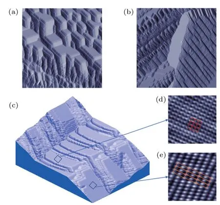
Fig.1.Morphology of YbMnBi2.Typical large-scale STM topographic images of YbMnBi2: (a) 100 nm×100 nm, 500 mV, 100 pA and (b)250 nm×250 nm, 500 mV, 100 pA. In order to enhance the visibility,dz/dx images are presented. (c)STM image(93 nm×69 nm,100 mV,500 pA)of YbMnBi2 with terrace and incline in three-dimensional representation. (d)and(e)Atomically-resolved STM topographic images(6 nm×6 nm,50 mV,5 nA)of terrace and incline of YbMnBi2,respectively. The images are taken at the square area marked in(c). Multiple unit-cells are labeled with red and orange rectangles. Different surface configurations are apparently discerned on two facets.
Figure 1 presents the typical morphology of the cleaved samples. Rather than a flat surface which is usually observed on a van der Waals bonded layered material, our YbMnBi2samples show rough morphology. As shown in Figs. 1(a)and 1(b), the surface exhibits terraces with small sizes and abrupt steps,which look like a staircase. In order to intuitively demonstrate the surface morphology of our YbMnBi2sample,we use a three-dimensional representation(Fig.1(c)).A series of terraces can be found at the center of the image,which are connected with inclines on their two sides. A flat surface usually gives rise to atomically resolved images in STM measurement, but a rough surface apparently is more difficult to image. On our sample,with a great care,we are able to successfully detect atom lattices both on terrace and incline,which are shown in Figs.1(d)and 1(e),respectively.
3. Discussion
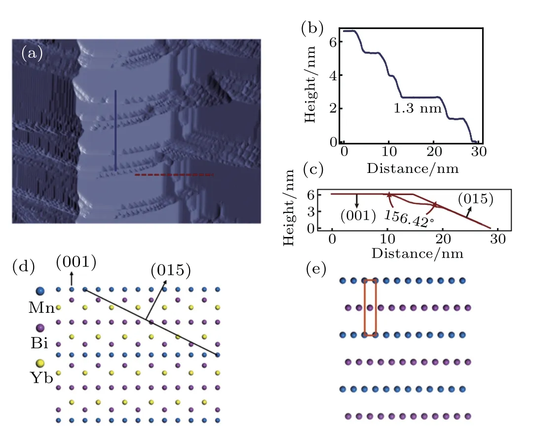
Having the morphology in mind, we next seek to understand the different facets. Figure 2(a) is the two-dimensional representation of Fig.1(c). The solid line crosses several terraces. The line profile in Fig. 2(b) clearly shows that all of the steps possess a height of about 1 nm,which is exactly the length of the unit vector c of a YbMnBi2crystal.Additionally,we have observed that the lattice on a terrace manifests itself as a square mesh with a side length of 0.47 nm. Since the lattice constants a and b of YbMnBi2are both 0.45 nm. We conclude that the terrace is the(001)facet. More insightfully,through the profile(Fig.2(c))of the dashed line that traverses terrace and incline,we reveal the angle between two surfaces is about 156°. Combined the angle with the atomic structure of YbMnBi2(Fig.2(d)),the(015)facet is the convincing orientation for the incline. Furthermore,the atomically-resolved image of incline in Fig. 1(e) corresponds to the schematic illustration of YbMnBi2(015) surface (Fig. 2(e)). The Mn atoms are located at the corners of the rectangle unit cell,and the Bi atoms occupy the face center. The measured short side length of the unit cell is 0.47 nm, accord with the (015)surface. Whereas, the experiment value of the long side is 1.6 nm,which is somewhat different from the bulk lattice constant 2.4 nm, we temporally attribute such a difference to the measuring error generated by the large angle between two surfaces. Up to now, we verify that the terrace and incline are(001)and(015)surface orientations of YbMnBi2.

Fig. 2. Schematic illustrations of different facets of YbMnBi2. (a) Same STM image with Fig. 1(c) in two-dimensional representation. (b) and (c)Height profiles along the blue solid line and red dashed line in(a), respectively. (d)Side view of the atomic structure of YbMnBi2. (001)and(015)surface orientations are labeled. Blue, purple, yellow balls stand for Mn,Bi, Yb atoms, respectively. (e) Atomic configuration of YbMnBi2 (015)surface. The orange rectangle represents the surface unit cell.
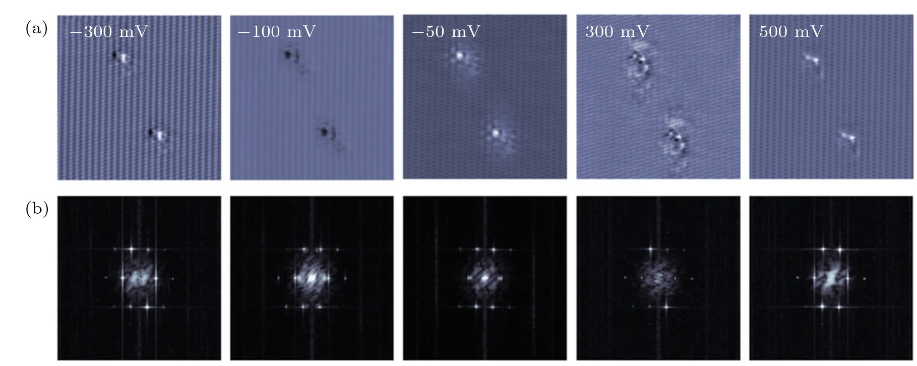
QPI measurement is a powerful method to detect the scattering property of the charge carriers on a surface of a topological material.[56-60]A QPI map requires the surface electron to form a certain type of two-dimensional standing wave,usually around point defects. However,unfortunately on our samples,the (001) facet only occurs in a small area. We have not observe any defects on the(001)facets. On the vicinal surface,we indeed detect a area with atomically flat morphology with two point defects on it.As demonstrated in Fig.3,we present a series of dI/dV maps at indicated voltages.The patterns from the two defects at various energies(voltages)appear identical to each other, indicating that they are the same defects. In a wide range of voltages, we do not observe periodical ripples around the defects,thus can not draw any conclusion based on the analysis of standing wave.Thus the QPI type measurement is waiting for future investigation.

Fig. 3. Quasiparticle interference on YbMnBi2 (015) surface. (a) Voltage-dependent dI/dV maps (20 nm×20 nm, 500 mV, 2 nA) and (b)Fourier transformed dI/dV maps at an area with two same defects on YbMnBi2 (015)surface.
4. Summary
In our STM experiment on vacuum cleaved YbMnBi2samples, we find that our samples possess very few amount of defects,thus are of high quality. But the morphology after cleaving is very rough,which renders the QPI type of measurement. We determine that the terrace on the surface is (001)oriented and the incline is (015) facets. The hill and valley morphology is believed to come from the non-layer nature of the crystal structure. Our results provide some guide for the future investigation of the type-II magnetic Weyl semimetal YbMnBi2. In order to obtain a large area of flat(100)surface,a more complicated surface technology,such as sputtering and annealing,is required.
- Chinese Physics B的其它文章
- Coercivity mechanisms in nanostructured permanent magnets∗
- Progress in recycling of Nd-Fe-B sintered magnet wastes∗
- Grain boundary restructuring and La/Ce/Y application in Nd-Fe-B magnets∗
- Topology of triple-point metals∗
- Local evolutions of nodal points in two-dimensional systems with chiral symmetry∗
- Structural,elastic,and electronic properties of topological semimetal WC-type MX family by first-principles calculation∗

