
Effect of Ga on microstructure and properties of Sn-Zn-Bi solder for photovoltaic ribbon
2019-04-16 02:12:16ZhangMinXuHuanruiWangGangZhuZiyue
China Welding 2019年4期
Zhang Min,Xu Huanrui,Wang Gang,Zhu Ziyue
School of Materials,Xi′an University of Technology,Xi′an 710048,China
Abstract In this study,SEM,EDS,XRD and other test methods were used to study the effects of different Ga contents(0~2 wt.%)on microstructure,electrical conductivity,spreading area and mechanical properties of Sn-9Zn-3Bi solder.The results revealed that the microstructure of Sn-Zn-Bi-Ga solder alloy was mainly composed of β-Sn,Zn-rich,Bi-rich phase and Sn-Zn eutectic structure.The Ga can significantly improve the wettability of Sn-Zn-Bi on the pure copper,the maximum wetting area was 105.3 mm2.With the increase of the Ga content the melting point of the solders decreased from 195 ℃ to 177 ℃.In addition,the Ga element can increase the oxidation resistance of solder.Its conductivity showed a decreasing trend with the gradual increase of the Ga content.With the increased of the Ga content the IMC(Intermetallic Compound)of Sn-Zn-Bi-xGa/Cu is only Cu5Zn8 and its thickness decreased remarkably.
Key words Sn-Zn-Bi-Ga solder,microstructure,wetting area,intermetallic compound
0 Introduction
Monocrystalline silicon and polycrystalline silicon solar cell technologies are becoming the main products of the photovoltaic(PV)market due to their low cost and high efficiency production scenarios[1].Photovoltaic ribbons which also known as tinned copper strips are used primarily to connect solar panels in series to form a giant accumulator.However,the high melting point of the non-lead solder will generate strong thermo-mechanical stress during the soldering process,which makes the PV module susceptible to brittle fracture during later use and reduces the service life of the solar panel[2].Therefore,the choice of low melting point solder has profound implications for the soldering process of solar panels.Sn-Pb solder alloy is widely used due to its excellent wettability,low melting point(183 ℃),high electrical conductivity,good processability,excellent mechanical properties and low price[3-5].However,Pb and Pbcontaining compounds have been listed by the environmental protection agency(EPA)as one of the top 17 chemicals that pose the greatest threat to humans and the environment[6-8].The ban on the use of lead-containing solders was implemented by the EU on July 1,2006[6].Although there is no clear regulation in the photovoltaic industry at present,the development of green energy is the current trend,so the development of lead-free low-melting solder is imminent.
At present,lead-free solder mainly includes Sn-Ag and Sn-Cu[9-10].However,Ag and Cu are high melting point elements,the photovoltaic panel itself is sensitive to high temperature,thus limiting the application of the two alloy solders.The eutectic temperature of Sn-Zn solder is 198 °C,which is higher 15 ℃ than the Sn-Pb eutectic temperature.In addition,Sn-Zn solder has good mechanical properties and low cost[11-13].However,the liquid Sn-Zn solder has a high surface tension and zinc oxide floating on the liquid surface,resulting in poor wettability of the solder on the copper[14].Studies have shown that the addition of Bi in the Sn-Zn solder improves the wettability and mechanical properties of the Sn-Zn alloy and further reduces the melting point of the alloy.However,excessive Bi element is prone to segregation at the junction of solder and Cu,resulting in a sharp drop in the mechanical properties of the solder joint[15-16].
Liu et al.[17]found that the addition of Ga element in Sn-8.5Zn-0.5Ag-0.1Al lead-free solder reduced the wetting time and wetting angle of the solder,while the wetting force increased.Wang et al.[18]thought that the addition of the Ga to the Sn-Zn-Bi solder reduces the thermal stress and resistivity of the welded joint.Ren et al.[19]found that the addition of Sb element to Sn-8Zn-3Bi can refine the grain and improve the mechanical properties of th solder.Billah et al.[20]found that Ni element can refine grains and further improve the mechanical properties such as tensile strength and hardness of brazing filler metal.Zhou et al.[21]found that the addition of Nb to Sn-8Zn-3Bi not only improved the wetting properties of the solder,but also improved the mechanical properties and oxidation resistance of the solder.Chen et al.[22]found that adding the Ga element to Sn-Zn solder can improve the wetting property and oxidation resistance of solder.
The solder/Cu bonding layer has a decisive influence on the tensile strength of the solder.Studies have shown that[23-24],when the Zn content is less than 0.5wt.%,the intermetallic compound(IMC)is Cu6Sn5,and when the Zn content is between 0.5-1.0 wt.%,the IMC is mainly Cu5Zn8and Cu6Sn5bilayer structure.When the Zn content exceeds 1wt.%,the IMC is Cu5Zn8,and the thickness of IMC increases with the increase of Zn content.Lee et al.[25]found that IMC was the main source of stress.The thicker the IMC,the higher the stress of the welded joint,which led to cracks in the IMC and affected the weldment performance.
The current report on the effect of the Ga on Sn-9Zn-3Bi alloy and its weldability have not been found.Therefore,the effects of the Ga element on the microstructure,wetting properties and brazing bond interface of Sn-9Zn-3Bi solder are studied.Thus,the optimal distribution ratio of the lead-free solder photovoltaic strip is obtained.
1 Experiment
In this study,pure Sn,Zn,Bi,Ga(99.99%)were used to smelt solder alloy of Sn-9Zn-3Bi-xGa(x=0.1,0.3,0.5,1.0,2.0 wt.%).The melting temperature was set to 550 ℃,and cooling after 30 min of heat preservation in air.
The cast sample was prepared into a cylinder ofϕ25 mm×5 mm,and the electrical conductivity was measured by taking 8 points using a FQR-7501A eddy current conductivity meter.The solder wetted sample was carried out on a 40 mm×40 mm×1 mm copper plate.The wetting temperature was set toTm(melting point)+50 ℃.Three sets of samples were taken for the same component,and 0.5±0.001 g of the sample was weighed each time.Measurements were made and ZnCl2+NH4Cl flux was used.The cast sample and the wetted sample are respectively prepared into a metallographic sample of 10 mm×10 mm×5 mm and a solder joint sample of 10 mm×5 mm×2 mm.4%HNO3+1%HCl+95%Alcohol was used to deal with samples.The DSC200F3 differential scanning calorimeter(DSC)and thermogravimetric analyzer(TGA)were used to test the melting point and oxidation resistance of the solder alloy.The heating rates were set to 10 K/min and 5 K/min,respectively.Protected with nitrogen and the TGA is cooled in an air atmosphere.The XRD-7000S X-ray diffractometer(XRD)was used to analyze the cross-section room temperature composition of the brazed joint.The scanning range was set to 20°-95° and the step length was 10 °/min.The experimental operation is carried out according to GB/T11363-2008 "Brazing joint strength test method" for tensile specimen preparation,using HT-2402 computer servo control material testing machine,its tensile rate is 2 mm/min,its tensile specimens such as Fig.1.
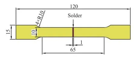
Fig.1 Drawing diagram of Sn-9Zn-3Bi-xGa/Cu(mm)
2 Experimental results and analysis
2.1 Influence of Ga on microstructure
Fig.2 is a backscattered electron map(BSE)of the microstructure of a Sn-9Zn-3Bi-xGa solder alloy.It can be observed that the microstructure of the solder was mainly composed of four different phases.The composition analysis of Fig.2a-Fig.2d was carried out by EDS.EDS results were shown in Table 1.The analysis indicated that the microstructure consists mainly of gray Sn matrix phase,black needle-like microstructure rich in Zn phase,white granular structure as Bi-rich phase and striped structure as Sn-Zn eutectic structure.
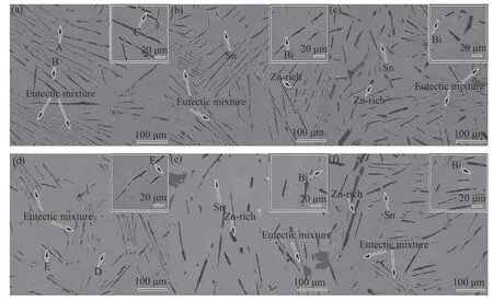
Fig.2 Microstructures of Sn-9Zn-3Bi-xGa(a)0 Ga(b)0.1Ga(c)0.3 Ga(d)0.5 Ga(e)1.0 Ga(f)2.0 Ga
It can be seen that the Ga element had a significant effect on the microstructure.When the Ga content is 0.1 wt.%,the Zn-rich phase is longer and thicker,and the eutectic structure is evenly spaced,but the change of microstructure was not obvious compared to 0 wt.% Ga solder.With the further increase of the Ga content,the acicular Znrich phase in the brazing material gradually broke and coarsened,and the eutectic structure gradually became sparse.When the Ga content is 0.5 wt.%,The Zn-rich phase was the finest and the eutectic structure distribution became larger.When the Ga content was 1.0 wt.%,the Zn-rich phase appeared to coarsen again.When the Ga content was 2.0 wt.%,the Zn-rich phase was segregated.It can be seen from the binary phase diagrams of Sn-Ga,Zn-Ga,and Bi-Ga that the Ga did not form a compound with Sn,Zn and Bi separately,but existed in a solid solution form.According to the Hume-Rothery criterion[26],if the electronegativity difference between the constituent alloy elements was greater than 0.4 wt.%,a stable intermediate phase can be formed,but if the electronegativity difference was smaller,the solid solution tended to be formed.The electronegativity of Sn,Zn and Bi were 1.96,1.65 and 2.02,respectively,and theelectronegativity of the Ga was 1.81.Therefore,it was known that the Ga element existed mainly in solid solution in other phases
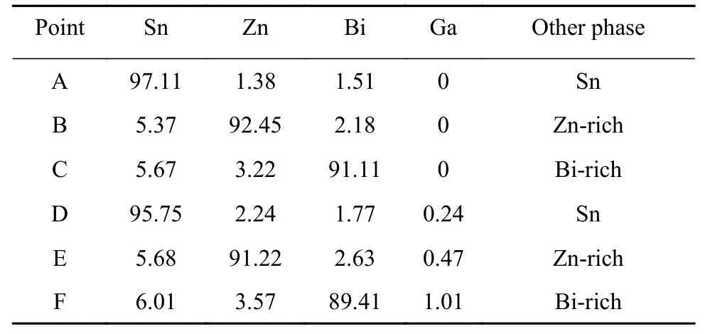
Table 1 EDS component analysis of Sn-9Zn-3Bi-xGa(wt.%)
2.2 Influence of Ga on wetting properties
The excellent wettability of the solder played a crucial role in the fabrication of the photovoltaic strip.If the wettability of the solder was too poor,the solder cannot be properly connected with the copper strip.

Fig.3 Solder alloy spreading area
The spread area of Sn-Zn-Bi-xGa solders were showed in Fig.3.It can be observed that with the Ga content increased,the spread area of the solder increased first and then decreases.The maximal wetting area was 105.3 mm2when the Ga content was 0.5 wt.%.the Ga was a surface active element,which was concentrated on the phase interface of the liquid solder and changes the composition and structure of the surface of the liquid solder,greatly reduced the interfacial tension,and the fluidity was significantly improved.Li et al.[27]found that the Ga element was usually concentrated on the surface of the alloy and gradually decreased from the outside to the inside by AES(auger electron spectroscopy)research.From the thermodynamic point of view,the free energy of Ga2O3(-998.3 kJ/mol)was much lower than ZnO(-320.5 kJ/mol),so Ga2O3was more stable than ZnO and was preferentially formed.Therefore,when the Ga element is enriched in the surface of the graphite material to form Ga2O3,the further contact of the molten metal material and the oxygen is effectively isolated,so that the wetting property of the graphite material is increased.
2.3 Influence of Ga on DSC,TGA
In the process of brazing precision instruments,especially PV modules,if the melting point of solder is too high,the PV modules will be damaged.Therefore,the low melting point solder is the first choice in the process of welding PV modules.Fig.4 shows the results of DSC and TGA test of solder alloy.
As the Ga content was from 0 wt.% to 2.0 wt.%,the melting point of the solder decreased from 195 ℃ to 177 ℃,when the Ga content was 0.5 wt.%,the melting point was close to Sn-Pb eutectic solder.The main reason for the decrease of the melting point of the Ga element is that Ga itself is a low melting point metal having a melting point of 29.8 ℃.During the smelting process,the Ga element was dissolved in the Sn and Zn phases,resulting in a decrease in the melting point of the solder.
Fig.4b shows that the addition of the Ga contributes to the improvement of the oxidation resistance of the solder.When the Ga content is 0.5wt.%,the weight gain of the solder is minimal,and it is known that the Ga element can improve the oxidation resistance of the solder alloy.However,when the Ga content exceeds 0.5 wt.%,the quality of the solder decreases at the beginning of heating,which is because the melting point of the Ga element is too low,and volatilization occurs during heating,thereby causing a decrease in the quality of the solder.
2.4 Influence of Ga on conductivity
Conductivity is another criterion for evaluating the quality of photovoltaic strips.Too poor conductivity leads to an increase in the resistance of the PV strip,which results in a large consumption of electrical energy during the transfer process.At the same time,excessive resistance will cause the temperature of the photovoltaic ribbon to rise during the transfer process,which will make the thickness of the intermetallic compound of the welded joint thicker,and finally cause the tensile strength to decrease and damage the solar panel.

Fig.4 Sn-9Zn-3Bi-xGa Solder alloy(a)DSC(b)TGA
Fig.5 is a graph showing the conductivity of the solder alloy.As the content of the Ga increases,the electrical conductivity of the alloy gradually decreases.When the Ga content is 0 wt.%,0.1 wt.%,0.3 wt.%,0.5 wt.%,1.0 wt.%,2.0 wt.%,the electrical conductivity of the solder is 7.72 Ms/m,7.64 Ms/m,7.55 Ms/m,7.47 Ms/m,7.26 Ms/m respectively compared with 7.86 Ms/m of Sn-9Zn-3Bi,which decreased by 1.78%,2.79%,3.94%,4.96%,and 7.63%,respectively.

Fig.5 Sn-9Zn-3Bi-xGa alloy material alloy conductivity
Generally speaking,the main factors affecting the conductivity are lattice distortion,grain boundary,vacancy and other crystal defects,and the influence of solid solution on conductivity is more significant than that of the second phase.At room temperature,the Ga element is mainly solid.The dissolved form is present in the Sn,Zn phase,thus causing an increase in the resistivity of the solder,thereby degrading the electrical conductivity of the solder.
2.5 Influence of Ga on interface
The IMC is formed by the fact that the solder and the atoms in the copper substrate are diffused and bonded to each other by heating during the brazing process,thereby forming an intermediate bonding layer between the solder and the Cu substrate.The IMC itself is brittle compared to the solder,so the smaller the IMC thickness,the stronger the bond.If the IMC is too thick,it will generate excessive stress concentration during the thermal cycle,thus reducing the solder and the Cu substrate.The bonding strength even causes the entire solder body to relax,which affects the normal use of the photovoltaic ribbon.
Fig.6 is a BSE diagram of the Sn-9Zn-3Bi-xGa/Cu bonding interface.It can be seen from the figure that the thickness of the IMC gradually decreases with the increase of the Ga content.When the Ga content is greater than 1 wt.%,the IMC thickness stable.In addition,the addition of the Ga element reduces the crack on the IMC.When the Ga content is 0.5 wt.%,the IMC is the most flat and there is no crack formation,but as the content of the Ga continues to increase,the crack reappears.

Fig.6 Sn-9Zn-3Bi-xGa/Cu welding cross-section microstructure(a)0 Ga(b)0.1 Ga(c)0.3 Ga(d)0.5 Ga(e)1.0 Ga(f)2.0 Ga
3 Conclusions
The effects of the different Ga contents(0-2.0 wt.%)on the microstructure and properties of Sn-9Zn-3Bi solder were investigated.The Ga element can improve the overall performance of Sn-9Zn-3Bi solder.The conclusions are as follows:
(1)The microstructure of Sn-Zn-Bi-Ga brazing alloy is mainly composed of β-Sn,Zn-rich,Bi-rich phase and Sn-Zn eutectic structure,and the structure of the intermetallic compound layer of Sn-9Zn-3Bi-xGa/Cu joint is Cu5Zn8phase,and its thickness decreases with the increase of the Ga content.
(2)With the increase of the Ga content,the wetting area of solder on copper sheet increases first and then decreases.When the content of the Ga is 0.5wt.%,the wetting area on pure copper increases 37.64% compared with Sn-9Zn-3Bi(76.5/mm2).At the same time,the Ga element also contributes to the decrease of solder melting point.With the content of the Ga from 0-2 wt.%,the melting point of brazing metal decreases from 195 ℃ to 177 ℃.The Ga element also improves the oxidation resistance of the filler metal.
- China Welding的其它文章
- Fabrication of in-situ synthesized ceramic reinforced Ni-based alloy composite coatings by reactive braze coating processing
- Electron beam welding of SiCp/2024 and 2219 aluminum alloy
- Seam-tracking based on dynamic trajectory planning for a mobile welding robot
- Combine S-N curve and fracture mechanics for fatigue life analysis of welded structures
- Graphene-coated copper foam interlayer for brazing carbon/carbon composite and niobium
- Analysis of weld pool vibration characteristics in pulsed gas metal arc welding