Improving The Performance of Inverted Planar Heterojunction Perovskite Solar Cells via Poly(n-vinylcarbazole) as Additive in Electron Transporting Layer
MIAO Ya,DONG Su-juan,LIU Shao-wei,WANG Ya-ling,YANG Yin,CAO Huan-qi,QIN Wen-jing,YANG Li-ying*,JI Wei-wei,YIN Shou-gen*
(1.Key Laboratory of Display Materials and Photoelectric Devices,Education Ministry of China,Tianjin University of Technology,Tianjin 300384,China; 2.Tianjin Key Laboratory for Photoelectric Materials and Devices,School of Materials Science and Engineering,Tianjin University of Technology,Tianjin 300384,China; 3.School of Chemical Engineering and Technology,Tianjin University,Tianjin 300072,China; 4.China Electronics Technology Group Corporation No.18th Research Institute,Tianjin 300384,China)
Improving The Performance of Inverted Planar Heterojunction Perovskite Solar CellsviaPoly(n-vinylcarbazole) as Additive in Electron Transporting Layer
MIAO Ya1,2,DONG Su-juan1,2,LIU Shao-wei1,2,WANG Ya-ling1,2,YANG Yin1,2,CAO Huan-qi1,2,QIN Wen-jing1,2,YANG Li-ying1,2*,JI Wei-wei3,4*,YIN Shou-gen1,2*
(1.KeyLaboratoryofDisplayMaterialsandPhotoelectricDevices,EducationMinistryofChina,TianjinUniversityofTechnology,Tianjin300384,China; 2.TianjinKeyLaboratoryforPhotoelectricMaterialsandDevices,SchoolofMaterialsScienceandEngineering,TianjinUniversityofTechnology,Tianjin300384,China; 3.SchoolofChemicalEngineeringandTechnology,TianjinUniversity,Tianjin300072,China; 4.ChinaElectronicsTechnologyGroupCorporationNo.18thResearchInstitute,Tianjin300384,China)
An electron-rich poly(n-vinylcarbazole) (PVK) was applied to dope the [6,6]-phenyl-C61-butyric acid methyl ester (PCBM) to explore the influence of PVK on the electron transfer layer of planar heterojunction perovskite solar cells.Under the optimized PVK doping mass fraction of 4%,the power conversion efficiency (PCE) of the CH3NH3PbI3perovskite solar cells is enhanced from (5.11±0.14)% to (9.08±0.46)%.According to the surface morphology study of the electron transport layer,PVK doping improves the coverage and quality of PCBM layer onto the rough perovskite layer,and this is beneficial for the interfacial contact of the CH3NH3PbI3,PCBM films and the top Al electrode,which results in the decrease of leakage current.Moreover steady-state PL analysis shows that the electron-rich PVK have a better passivation effect on the trap states at the perovskite surface or crystal boundaries as a material of interfacial modification of cathodes,thus can apparently decrease the charge recombination of the perovskite solar cells.
perovskite solar cells; doping; interface engineering; poly(n-vinylcarbazole); trap states
1 Introduction
Inorganic-organic hybrid perovskite solar cells have become increasingly popular owing to the excellent properties such as high absorption coefficients[1],ambipolar carrier transport properties[2],tunable band gaps[3],long excitions diffusion lengths over 100 nm[4],high defect tolerances[5].Its power conversion efficiency (PCE) has increased from 3.8% to 22.1% in the past seven years[6-11].In general,perovskite solar cells are based on a mesoscopic or planar heterojunction structures.The conventional mesoscopic architecture shows remarkable performance,but the high temperature sintering of meso-TiO2layer could increase the cost of manufacture and incompatible with the flexible substrates,which limit its application.The inverted planar heterojunction perovskite solar cells with the structure of ITO/PEDOT:PSS/perovskite/electron transporting layer (ETL)/cathode have been becoming more and more attractive because of hysteresis-lessJ-Vcharacteristics due to the effectively trap passivation of fullerene derivative and some other unique advantages such as easy-fabrication and cost-effectiveness characteristics[12-16].PCBM is the most commonly used ETL materials in this device.However,the poor film-forming performance of PCBM is difficult to form a completely film on the rough surface of perovskite.For this problem,several research groups have devoted efforts to optimize the device.Zhangetal.used PCBC as cathode buffer layer greatly improved the photovoltaic performance[17].Baietal.fabricated perovskite solar cells by adding high molecular weight polystyrene into the PCBM solution.The addition increases the viscosity of the PCBM solution,thus improves the quality of the ETL films[18].Zhuetal.found that an amine-containing polymeric semiconductor (PFNOX) doped PCBM layer promoted the electron injection from perovskite into the ETL and suppressed the charge recombination[19].In our previous work,we have developed polyethylenimine (PEI) containing alkyl amine side chain as additive to modify the PCBM layer[20].It was discovered PEI could enable effectively electron transfer between the perovskite layer and the cathode.The effective electrical doping of PEI to PCBM inspired us to use electron-rich polymer PVK as additive to dope the PCBM ETL for perovskite solar cells.In this paper,we report PVK as additive doping in the PCBM ETL to enhance the performance of perovskite solar cells.Atomic force microscopy (AFM) and PL measurements were used to characterize the ETL layers.The function of PVK can be summarized as follows.First,PVK can increase the viscosity of the PCBM solution thus enhance the film-forming performance of PCBM,as well as optimize the morphology of perovskite/PCBM and PCBM/Al interfacial.Additionally,the nitrogen atom of the PVK is also electron-rich,it can donate a lone pair electrons to the Pb,thus efficiently passivate the perovskite crystal trap states.
2 Experiments
2.1 Reagents and Materials
2.2 Device Fabrication and Characterization
The PEDOT:PSS layer was spin-coated on the pre-cleaned ITO substrates.PbI2solution of 231 mg/mL in DMF was stirred at 70 ℃ for 5 h,filtered with a 0.22 μm nylon membrane before spin-coated.The PbI2layer was spin-coated on the PEDOT:PSS substrates which were preheated to 50 ℃ at 6 000 r/min for 30 s,followed by annealing on a 70 ℃ hot plate for 10 min.CH3NH3I with a concentration of 38 mg/mL in IPA was dissolved at ambient temperature for 4 h,then filtered with a 0.45 μm PVDF membrane.The CH3NH3I solution was spin-coated on the PbI2film at 6 000 r/min for 20 s after reaction for 30 s,followed by annealing on a 60 ℃ hot plate in air for 10 min then 100 ℃ for 20 min.The thickness of the CH3NH3PbI3layer is about 260 nm.PCBM solution of 24 mg/mL in o-DCB was dissolved at 60 ℃ for 14 h,add the PVK to the PCBM solution to form a blend solution.The PCBM films doped with or without PVK additive were spin-coated onto the perovskite layer at 1 000 r/min for 60 s which have a thickness about 40 nm,after that the films were transported into an Ar-filled glove box.Finally,Al metal electrode which has a thickness about 100 nm was deposited.During deposition,the film was masked by a metal shadow mask determined the cell with active area of 0.10 cm2.
The current density-voltage (J-V) curves of the un-encapsulated photovoltaic devices were characterized by a programmed Keithley 2400 source-meter unit under illumination of a Newport Oriel 150 W solar simulator (AM1.5G,100 mW·cm-2).The light intensity of the solar simulator was calibrated with a solar reference cell (SRC-1000-TC-QZ,VLSI standards,Inc.).The surface morphology of the CH3NH3PbI3,CH3NH3PbI3/PCBM and CH3NH3PbI3/PCBM+ (1%-6%) PVK layers was investigated by AFM (Bruker INNOVA®SPM) in tapping mode.Steady-state PL was measured by a Jobin Yvon Fluorolog-3 fluorescence spectrometer.The thickness of the above films was recorded by a KLA-Tencor Alpha-Step D-100 surface profiler.More detailed information can be found in our previous paper[20].
3 Results and Discussion
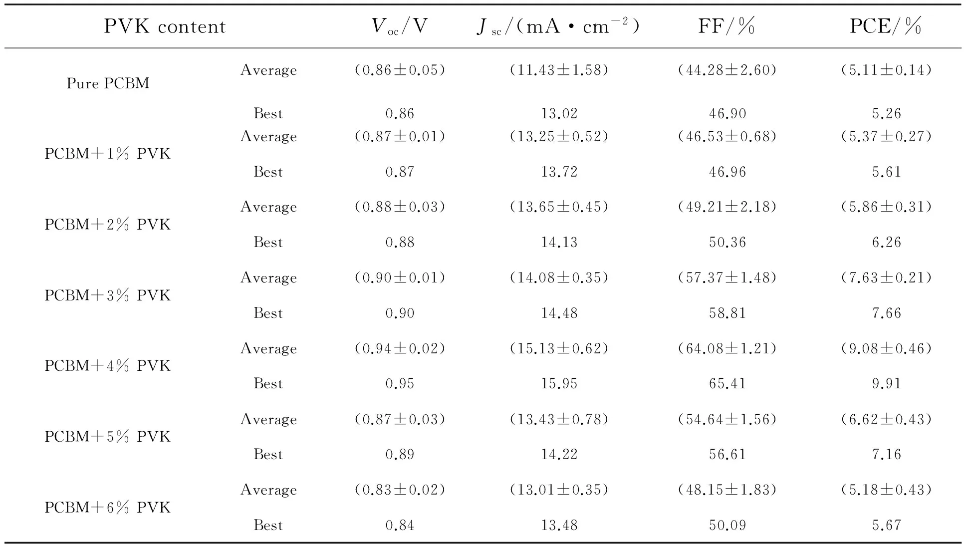
Fig.1(a) and Fig.1(b) present the molecular structures of PCBM,and PVK.Here we fabricated inverted perovskite solar cells with the structure of ITO/PEDOT:PSS/perovskite/PCBM:PVK/Al.The schematic diagram of the device structure and the energy levels of all functional layers are showed in Fig.1(c) and Fig.1(d).Fig.2(a) shows the current density-voltage (J-V) curves of the best pristine PCBM-based device and device with 4%(mass fraction) PVK doping measured in forward bias.Fig.2(b) shows theJ-Vcurves of the device with 4% PVK doping measured in forward and reversed directions.We can see that there is no apparent current hysteresis existing.The measured photovoltaic parameters of the devices are summarized in Tab.1.As showed in Fig.2(a) and Tab.1,compared to the pristine PCBM-based device,the addition of 4% PVK in PCBM increases theVOCfrom (0.86±0.05) V to (0.94±0.02) V,JSCfrom (11.43±1.58) mA/cm2to (15.13±0.62) mA/cm2,FF from (44.28±2.60)% to (64.08±1.21)%,and PCE from(5.11±0.14)% to (9.08±0.46)%.This efficiency enhancement can be attributed to the simultaneous increase of theVOC,JSCand FF.

Fig.1 (a) Molecular structure of PCBM.(b) Molecular structure of PVK.(c) Schematic device configuration.(d) Schematic energy level diagram of the device.

Fig.2 (a)J-Vcurves of CH3NH3PbI3devices for the best device with PVK and without PVK.(b)J-Vcurves for the ITO/PEDOT:PSS/perovskite/PCBM+4% PVK/Al in forward and reverse bias.

Tab.1 Photovoltaic parameters of the perovskite solar cells with various PVK content
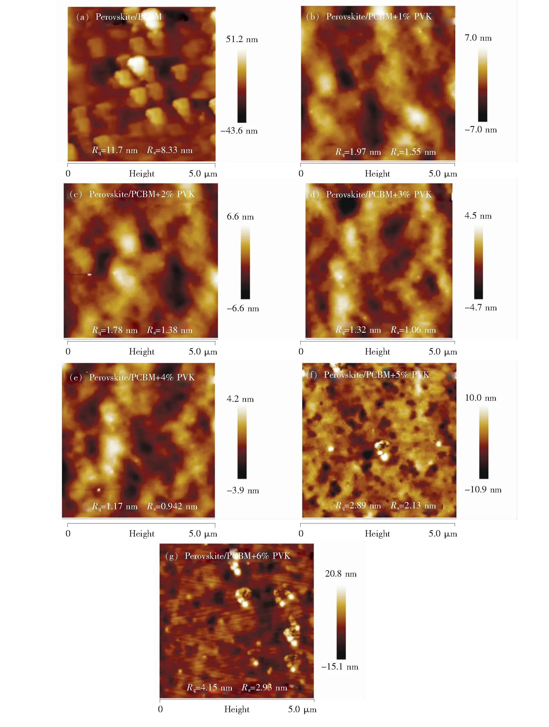
To further explore how the PVK influence the device performance,the surface morphology of PCBM and PVK doped PCBM films were measured by AFM.As shown in Fig.3,we can observe that the root mean square roughness (Rq) and mean roughness (Ra) of the PVK doped PCBM film are decreased compare to the pristine PCBM film on top of perovskite film.After doping 4% PVK in PCBM,theRqandRavalue are decreased from 11.7 to 1.17 and from 8.33 nm to 0.94 nm,respectively.Obviously,the addition of PVK can help PCBM solution to form a more smooth film on the rough surface of perovskite film.The reason is that PVK doping can increase the viscosity of PCBM solution which made it much easier to form a fully covered,uniform and compact ETL layer.Such a smooth surface is helpful to form Ohmic contact between PCBM and Al electrode,which is helpful to suppress the leakage current at the interfaces of the perovskite,PCBM film and the Al electrode,which promote the increase ofJSCandVOC.However,excessive addition of PVK led to irregular formation of PVK agglomeration.This may explain the decreased ofVOC,JSCand FF when the doping mass fraction of PVK up to 5% and 6%.
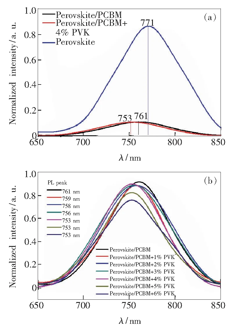
Due to low stability of the CH3NH3PbI3materials,there is a large concentration of trap states close to the top surface or grain boundaries of perovskite crystals.Huang and co-workers[22]reported that the trap states could induce band bending close to the surface of the CH3NH3PbI3film,which may cause a red shift of the PL peak.Here,an excitation wavelength of 360 nm was used to excite the film of CH3NH3PbI3/PCBM and CH3NH3PbI3/PCBM doped with PVK from the air side,respectively.The pure perovskite film ,PCBM or PCBM+1%-6% PVK covered CH3NH3PbI3films show the PL peak at 759,758,756,753,753,753 nm,respectively (Fig.4).The blue-shifted PL peak is obvious for the PCBM doped PVK increasing from 0 to 4%,which suggests that the doped PVK in PCBM can passivate the trap states close to the top surface of the perovskite film.So device performance (Jsc,Voc,FF) is improving with the increasing of doped PVK.These results revealed that when 4% PVK doped in PCBM shows a better passivation effect.The PL intensity with 5% and 6% PCBM doped PVK have a slight decline than the PCBM without PVK.The reason may be that the hole transporting property of PVK has a negative effect on the electronic transporting of PCBM.

Fig.3 AFM topography of the PCBM films without or with 1%-6% PVK coated on perovskite layer

Fig.4 Steady-state PL spectra of the perovskite,perovskite/PCBM,perovskite/PCBM+4% PVK films(a),and the perovskite/PCBM,perovskite/PCBM+1%-6% PVK films (b).
4 Conclusion
In summary,an electron-rich polymer,PVK,was introduced into perovskite solar cells for the first time by doping it in PCBM ETL,leading to an efficiency enhancement of the CH3NH3PbI3-based perovskite solar cells.Under the optimized PVK doping mass fraction of 4%,the PCE of the device is enhanced to (9.08±0.46)%.The surface morphology study of the ETL film shows that PVK doping improved the coverage and quality of PCBM ETL onto the rough perovskite layer and this is beneficial for the interfacial contact between the CH3NH3PbI3,PCBM films and Al electrode,which results in enhancement of hole blocking ability and decrease of leakage current.In addition,PL analysis reveals that the electron-rich PVK has a better passivation effect on the trap states at the perovskite surface or crystal boundaries,which facilitating the charge separation and suppressing the undesired charge recombination.Therefore,our work shows that electron-rich polymer can be used as an effective additive for the electron transporting layer PCBM,which provides an effective and convenient approach to enhance the performance of inverted planar heterojunction perovskite solar cells.
[1] LEE M M,TEUSCHER J,MIYASAKA T,etal..Efficient hybrid solar cells based on meso-superstructured organometal halide perovskites [J].Science,2012,338(6107):643-647.
[2] GIORGI G,FUJISAWA J I,SEGAWA H,etal..Small photocarrier effective masses featuring ambipolar transport in methylammonium lead iodide perovskite: a density functional analysis [J].J.Phys.Chem.Lett.,2013,4(24):4213-4216.
[3] EPERON G E,STRANKS S D,MENELAOU C,etal..Formamidinium lead trihalide: a broadly tunable perovskite for efficient planar heterojunction solar cells [J].EnergyEnviron.Sci.,2014,7(3):982-988.
[4] STRANKS S D,EPERON G E,GRANCINI G,etal..Electron-hole diffusion lengths exceeding 1 micrometer in an organometal trihalide perovskite absorber [J].Science,2013,342(6156):341-344.
[5] YIN W J,SHI T T,YAN Y F.Unique properties of halide perovskites as possible origins of the superior solar cell performance [J].Adv.Mater.,2014,26(27):4653-4658.
[6] KOJIMA A,TESHIMA K,SHIRAI Y,etal..Organometal halide perovskites as visible-light sensitizers for photovoltaic cells [J].J.Am.Chem.Soc.,2009,131(17):6050-6051.
[7] YU J C,KIM D B,BAEK G,etal..High-performance planar perovskite optoelectronic devices: a morphological and interfacial control by polar solvent treatment [J].Adv.Mater.,2015,27(23):3492-3500.
[8] ZHAO Y X,ZHU K.Organic-inorganic hybrid lead halide perovskites for optoelectronic and electronic applications [J].Chem.Soc.Rev.,2016,45(3):655-689.
[9] LI X,BI D Q,YI C Y,etal..A vacuum flash-assisted solution process for high-efficiency large-area perovskite solar cells [J].Science,2016,353(6294):58-62.
[10] BI D Q,TRESS W,DAR M I,etal..Efficient luminescent solar cells based on tailored mixed-cation perovskites [J].Sci.Adv.,2016,2(1):e1501170-1-7.
[11] SALIBA M,MATSUI T,SEO J Y,etal..Cesium-containing triple cation perovskite solar cells: improved stability,reproducibility and high efficiency [J].EnergyEnviron.Sci.,2016,9(6):1989-1997.
[12] WANG Q,SHAO Y C,DONG Q F,etal..Large fill-factor bilayer iodine perovskite solar cells fabricated by a low-temperature solution-process [J].EnergyEnviron.Sci.,2014,7(7):2359-2365.
[13] XU J X,BUIN A,IP A H,etal..Perovskite-fullerene hybrid materials suppress hysteresis in planar diodes [J].Nat.Commun.,2015,6:7081-1-8.
[14] SHAO Y C,YUAN Y B,HUANG J S.Correlation of energy disorder and open-circuit voltage in hybrid perovskite solar cells [J].Nat.Energy,2016,1:15001-1-6.
[15] 李建丰,赵创,张恒,等.利用PVP添加剂提高钙钛矿太阳能电池光伏性能 [J].发光学报,2016,37(1):56-62.LI J F,ZHAO C,ZHANG H,etal..Enhancement of the photovoltaic performance of CH3NH3PbI3perovskite solar cells by using polyvinylpyrrolidone additive [J].Chin.J.Lumin.,2016,37(1):56-62.(in English)
[16] ZHANG K C,YU H,LIU X D,etal..Fullerenes and derivatives as electron transport materials in perovskite solar cells [J].Sci.ChinaChem.,2017,60(1):144-150.
[17] LIU X D,JIAO W X,LEI M,etal..Crown-ether functionalized fullerene as a solution-processable cathode buffer layer for high performance perovskite and polymer solar cells [J].J.Mater.Chem.A,2015,3(17):9278-9284.
[18] BAI Y,YU H,ZHU Z L,etal..High performance inverted structure perovskite solar cells based on a PCBM:polystyrene blend electron transport layer [J].J.Mater.Chem.A,2015,3(17):9098-9102.
[19] ZHU Z L,XUE Q F,HE H X,etal..A PCBM electron transport layer containing small amounts of dual polymer additives that enables enhanced perovskite solar cell performance [J].Adv.Sci.,2016,3(9):1500353-1-7.
[20] DONG S J,WAN Y Y,WANG Y L,etal..Polyethylenimine as a dual functional additive for electron transporting layer in efficient solution processed planar heterojunction perovskite solar cells [J].RSCAdv.,2016,6(63):57793-57798.
[21] ETGAR L,GAO P,XUE Z S,etal..Mesoscopic CH3NH3PbI3/TiO2heterojunction solar cells [J].J.Am.Chem.Soc.,2012,134(42):17396-17399.
[22] SHAO Y C,XIAO Z G,BI C,etal..Origin and elimination of photocurrent hysteresis by fullerene passivation in CH3NH3PbI3planar heterojunction solar cells [J].Nat.Commun.,2014,5:5784-1-7.

妙亚(1988-),女,山东菏泽人,硕士研究生,2010年于聊城大学获得学士学位,主要从事钙钛矿太阳能电池的研究。
E-mail:miaoya9012@163.com

杨利营(1973-),男,河北石家庄人,博士,研究员,2002年于天津大学获得博士学位,主要从事有机光电功能材料与器件的研究。
E-mail: liyingyang@tjut.edu.cn
2017-02-27;
2017-04-22
国家自然科学基金(51402214,61504097); 天津市自然科学基金(17JCYBJC21000,14JCYBJC42800); 国家重点科学仪器设备发展项目(2014YQ120351); 天津教委项目(20140423)资助
在电子传输层中添加PVK提高钙钛矿太阳能电池的性能
妙 亚1,2,董素娟1,2,刘少伟1,2,王亚凌1,2,杨 银1,2,曹焕奇1,2,秦文静1,2,杨利营1,2*,纪伟伟3,4*,印寿根1,2*
(1.天津理工大学 显示材料与光电器件教育部重点实验室,天津 300384 ;2.天津理工大学材料科学与工程学院 天津市光电显示材料与器件重点实验室,天津 300384;3.天津大学 化工学院,天津 300072; 4.中国电子科技集团第18研究所,天津 300384)
为了探究PVK对倒置平面异质结钙钛矿太阳能电池电子传输层的影响,向电子传输层PCBM中添加了一种富电子的聚乙烯基咔唑(PVK)。采用原子力显微镜、PL光谱对薄膜进行了表征。实验结果表明:少量PVK的添加提高了覆盖在钙钛矿薄膜上PCBM层的平整度。当PVK的添加质量分数为4%时得到最佳器件效率,相比于纯PCBM作为电子传输层的器件,器件效率由(5.11±0.14)% 提升到(9.08±0.46)%。当PVK的添加质量分数大于4%时,粗糙度又趋于变大。PL光谱显示,少量PVK的加入使钙钛矿/电子传输层薄膜的PL强度降低,并使PL峰蓝移。研究表明:向PCBM中掺杂适量PVK能够改善钙钛矿/电子传输层/Al的界面接触,减少漏电流,并能够减少钙钛矿表面陷阱和晶界缺陷,减少电荷复合,从而提高了器件性能。
钙钛矿; 掺杂; 界面工程; 聚乙烯基咔唑; 缺陷
1000-7032(2017)09-1210-07
TM914.4 Document code:A
10.3788/fgxb20173809.1210
cals were used as
without further purification,including PVK (Aldrich),[6,6]-phenyl-C61-butyric acid methyl ester (PCBM,99%,Solenne BV),PbI2(99.9985%,Alfa Aesar),HI (57% aqueous solution,Alfa Aesar),CH3NH2(40% aqueous solution,J&K Chemicals Inc.),1,2-Dichlorobenzene (o-DCB,98%,Alfa Aesar),Dimethylformamide (DMF,99.9%,J&K Chemicals Inc.) and Isopropyl alcohol (IPA,99.7%,J&K Chemicals Inc.),CH3NH3I was synthesized in our lab and reported elsewhere[21].
*CorrespondingAuthors,E-mail:liyingyang@tjut.edu.cn;jww315@126.com;sgyin@tjut.edu.cn
Supported by National Natural Science Foundation of China (51402214,61504097); Natural Science Foundation of Tianjin (17JCYBJC21000,14JCYBJC42800); National Key Scientific Instrument and Equipment Development Project (2014YQ120351); Project of Tianjin Education Commission(20140423)

